
Abstract
In this work we demonstrate the possibility to realize a novel unconventional ITO-free organic light emitting diode (OLED) utilizing a photonic polymeric electrode. Combining electron beam lithography and a plasma etching process to partially structure the highly conductive poly(3,4 ethylenedioxythiophene):poly(styrene sulfonate) (PEDOT:PSS) it is possible to realize an embedded photonic crystal (PC) structure. The realized PC-anode drastically reduces the light trapped in the OLED, demonstrating the possibility to eliminate further process stages and making it easier to use this technology even on rollable and flexible substrates.
Export citation and abstract BibTeX RIS
1. Introduction
Organic LEDs will play a fundamental role in future OE (organic electronic) devices due to their achievements in efficiency, their ease of realization, and the possibility of making them on flexible substrates. One of the essential points to ensure the future development of this technology is the quantum efficiency, which gives this class of device a key role in innovative lighting. It is widely known that the external quantum efficiency of conventional organic LED devices remains close to 20% because of losses due to wave-guiding effects. Recently, there has been great progress in enhancing the efficiency of light out-coupling of organic electroluminescent devices by means of various internal and external device modification techniques. Several strategies have been developed concerning the surface modification to increase the efficiency factor, for example, by using ordered micro-lenses, Bragg reflectors, 2D photonic crystals or modifying the cavity effects [1–5].
One technological solution uses wrinkling of the emissive area, where even a doubling in the performance can be obtained due to a Bragg scattering effect [6]. Another technique makes use of two-dimensional nanopatterning to create a photonic crystal (PC), substantially improving the outcoupled light [7]. OLEDs and LEDs with a two-dimensional photonic crystal structure have been fabricated by several groups [7–10]. Patterned periodic subwavelength two-dimensional hole arrays were realized also on an optically thick aluminum (Al) film cathode [11]. To simplify the device architecture of 2D-PC OLEDs, a first effort on a partially structured ITO electrode was realized [12], showing an improvement in the light extraction efficiency for confined modes in ITO/organic layers due to the photonic crystal effect. More recently, an ITO electrode was partially patterned by a focused ion beam (FIB) in PEDOT:PSS, yielding a good increase of efficiency [13]. The relatively low refractive index of PEDOT:PSS [14] gives a high variation of the refractive index for the ITO–PEDOT:PSS structure, which is advantageous also on microstructured [15] or nanostructured grids [16]. Besides those inorganic electrodes, nanopatterned PEDOT:PSS—a widely used organic anode material for OLEDs due to its high work function, transparency and conductivity—is also of interest. Because of the challenge of patterning, the application of PEDOT:PSS nanostructures for devices has been very limited.
Here, for the first time to our best knowledge, we have realized a stacked OLED device with a 2D photonic crystal patterned polymeric anode electrode. We realized a photonic polymeric electrode using a plasma etching (PE) process to partially structure the highly conductive poly(3,4 ethylenedioxythiophene):poly(styrene sulfonate) (PEDOT:PSS) and we demonstrate how the final device performance is improved. We show different characterizations of the obtained structures and of the final device, quantifying the improvement obtained in terms of absolute values of luminance and efficiency.
2. Experimental details
The PC structure was fabricated using a high-resolution electron beam lithography (EBL) technique. The EBL facility employed consisted of a Raith 150 system. The samples were obtained by exposing a layer of ZEP (electronic resist) deposited on a highly conductive PEDOT:PSS layer, spin coated onto a Corning glass substrate. A 200-nm-thick layer of colloidal doped ZEP was spin coated on top of the cleaned substrate. Subsequently, the nanopatterning was defined using the Raith 150 system with a current and area dosage of 23.6 pA at 10 keV. The resist was developed in n-amyl acetate. The resulting two-dimensional photonic crystal is made of air rods embedded into the organic matrix of ZEP. A uniform triangular pattern consisting of rods of 220 nm diameter and with a period of 350 nm was made on a surface area of around 1.5 × 1.5 mm2.
The ZEP crystal was subsequently used as a lithographic mask during the anisotropic plasma etching process [17] of the underlying highly conductive PEDOT:PSS, which was obtained by doping the PEDOT:PSS with dimethylsulfoxide (DMSO), as described in a previous paper [18], and had a thickness of about 200 nm. The plasma etch partially removes the PEDOT:PSS layer, yielding a polymeric photonic crystal approximately 80 nm in height. The plasma process was performed in a high-vacuum PECVD multi-chamber system [19], fabricated by ELETTRORAVA, with the following parameters: power around 30W, 30 sccm for the O2, and pressure around 0.4 Torr for 80 s of treatment. As last step, N-metil-2-pirrolidone (NMP) solvent was used for ZEP removal without damaging the underlying PEDOT:PSS film.
The structure of the OLED device under investigation was: doped DMSO PEDOT:PSS 200 nm/NPD (N,N'-di-1-naphthaleyl-N,N'-diphenyl-1,1'-biphenyl-4,4'-diamine) 35 nm/CBP ((4,4'-bis(N-carbazolyl)-1,1'-biphenyl):Ir(Fppy) 3 (8%) Tris[2-(2,4-difluorophenyl)pyridine]iridium(III) 25 nm/BCP (bathocuproine) 10 nm/Alq3 (Tris-(8-hydroxyquinoline)aluminum) 10 nm/calcium 30 nm/aluminum 90 nm. The devices were fabricated on structured and unstructured PEDOT:PSS surfaces realized on the same substrate to prevent changes due to different growth conditions. In figure 1 is possible to follow the diagram of the process for the structured OLED device.
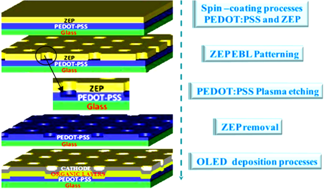
Figure 1. Schematic diagram of the process for the realization of the highly conductive PEDOT:PSS-PC anode and OLED device.
Download figure:
Standard image High-resolution imageCurrent–voltage (I–V) and electroluminescence–voltage (EL–V) characteristics have been measured, under nitrogen and ambient temperature, using a Keithley 2400 power supply sourcemeter with constant increment steps. Electroluminescence analysis was performed using a photodiode (Newport 818UV) connected to a Keithley 6517A Electrometer. The device electroluminescence spectra were evaluated through a CCD imaging telescope (OL610) connected to a spectroradiometer (OL770-LED).
An optical setup was finally adopted to evaluate the PC properties and estimate the OLED spectral properties. Light propagating in the glass substrate and extracted by diffraction was measured at room temperature using the setup reported in figure 2, This apparatus has been used to analyse the optical properties of our photonic crystals in order to evaluate the resonances of the structures and the operational optical ranges. Moreover, this experiment was repeated so as to analyse the optical responses of the entire OLED, with and without the unavoidable cathode wrinkling.
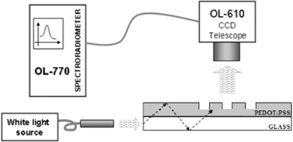
Figure 2. Optical setup employed for the PC evaluation and spectra measurements.
Download figure:
Standard image High-resolution image3. Results and discussion
After the PE process and the subsequent ZEP removal step, the PEDOT:PSS crystal structures (see figure 3(a)) were tested by introducing white light from the edge of the glass substrate that propagated inside the glass itself due to the total internal reflection phenomena, as shown in figure 2.
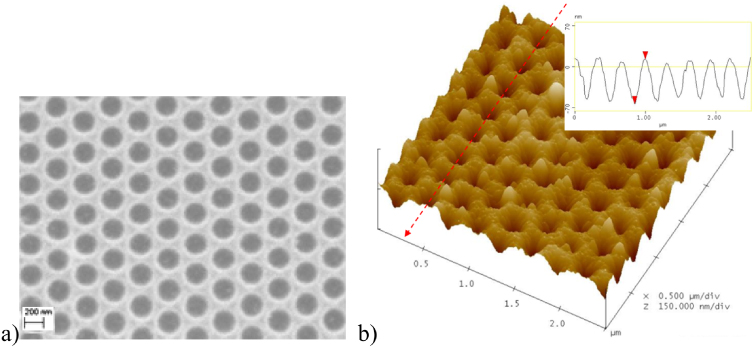
Figure 3. (a) SEM image of the PEDOT:PSS 2D PCs obtained after the ZEP removal step. (b) AFM image of the structured OLED cathode (the peak to valley measurement is around 77 nm).
Download figure:
Standard image High-resolution imageFigure 4 shows the spectrally integrated light intensity characteristics of the hexagonal PC as detected normal to the sample surface. Resonant peaks in the PEDOT:PSS crystal appear due to the PC feedback effect, with the full width at half maximum of the spectrum being 20 nm at the main peak, which is located at around 450 nm.
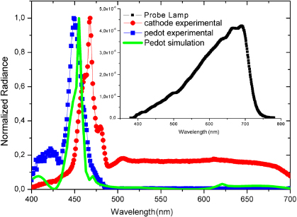
Figure 4. Intensity of light emitted from the PEDOT:PSS crystal (blue dot curve), the corresponding simulated spectrum (green line curve) and the the complete final OLED device spectrum (red dot curve). The inset shows the spectrum of the used test lamp related to the experiment reported in figure 2.
Download figure:
Standard image High-resolution imageIn order to verify our experimental findings we have calculated the resonant frequencies of the structures. We employed the finite-difference time-domain numerical method (FDTD) performed with commercial software (Full Wave simulation tool, RSoft Design Group, Ossining, NY). For simplicity, we assume that the glass substrate (Corning Eagle 2000) and the air are semi-infinite with constant refractive indices nglass = 1.51 and nair = 1, whereas a dispersion relation in the spectral region of interest has been used for the ITO and PEDOT:PSS. From figure 4, we can appreciate the suitability of the realization processes since the simulations approximate the spectra resulting from experimental measurements well.
We repeated the same experiment also on the final device to determine the effect that the structured PEDOT:PSS has on the device. The radiation was kept away from the other side of the glass substrate because it cannot pass through the cathode layer. In effect, it must be noted that the PC structure matches the shape between the anode and the cathode (see figure 3(b)), so the cathode reflectance also alters the electro-optical performance of the final device. In particular, figure 4 shows the variation of the peak extraction. Taking into account the spectrum of the test lamp used (see inset figure 4) it is easy to see that there is an improvement in photon extraction even at longer wavelengths. This can be underlined by observing how the bottom of the spectrum rises sharply as a percentage and how the spectral ramp reported in the inset of figure 4 is flattened.
These analyses help us understand how the variation in the electroluminescence spectrum of the final device is not easy to interpret, since it is a combination of several effects that produces the new spectrum. It is worthwhile underlining that the actual position of the electroluminescent film inside the OLED cavity is also crucial, especially in this case, in determining the final shape of the spectrum [20].
The OLED device was tested under a nitrogen atmosphere to prevent oxidation of calcium. The spectral evaluation suggests a spectral modification due to the PC pattern (see figures 4 and 5). The spectral modification, as already stated, can be ascribed to more than one cause because of the possibility of more than one photon-escaping mode. Our results are due not only to the PEDOT:PSS crystal but also to wrinkling of the resulting cathode, which can be observed by changing the angle at which the spectra are captured. To better investigate the resonance behaviour of our device we measured the angular spectrum (figure 5). For such a characterization, the radiation profiles were analysed through a polar angle dependent emission power measurement with measurements made on the sample at different light detection angles. In figure 5 it is possible to see that the contribution due to the photonic crystal becomes more and more important at high angles (in this case 40° and 45°), shifting the output spectrum towards lower wavelengths until it reaches the position of the extraction peak of the PEDOT:PSS crystal. This is mainly due to the change in the PC extraction efficiency with angle, which also modifies the angular distribution from the Lambertian one [21].
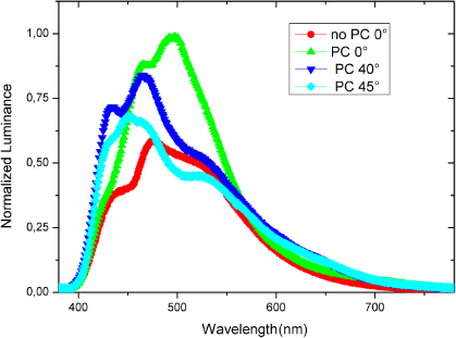
Figure 5. The spectrum of the unstructured (no PC) and structured (PC) devices (at 0.2 mA) captured at different angles.
Download figure:
Standard image High-resolution imageFrom figure 5 is possible to observe clearly the photonic crystal lateral lobes effect, which in this case turns into a change of the emitted light spectra because the peak emission of the device does not coincide perfectly with the extraction peak of the photonic crystal (there is a difference of about 30 nm). With figures 4 and 5 it is possible to gain an understanding regarding the difficulty in overcoming the angular-dependent colour-shift that could appear in a corrugated device with respect to a planar one [22].
Figure 6 displays the current–voltage (J–V) characteristics of the devices. The turn-on voltages of all the devices are approximately the same, around 3 V. It is worthwhile noting, however, that the PC device results in higher current densities at the same voltage, which is consistent with previous papers [23]. This confirms another important advantage of corrugated OLEDs, which is to reduce the operating voltage and to improve the power efficiency. This phenomenon can be easily explained by the increase of the active area of the layers with the corrugated anode [23].
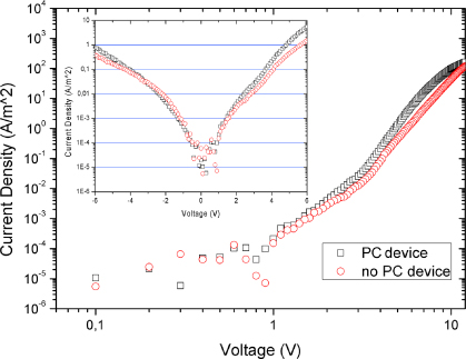
Figure 6. Current–voltage (J–V) characteristics of the devices. The inset reports J–V at reverse bias to control the current losses.
Download figure:
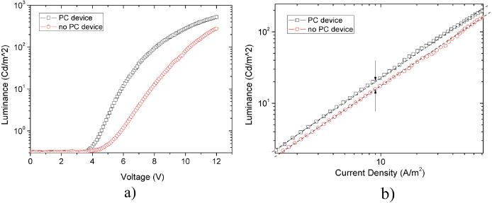
Standard image High-resolution imageFigure 7(a) shows the electroluminescence behaviour in terms of the luminance versus the applied voltage. The device with the structured PEDOT:PSS anode had the lowest optical switch-on voltage and the related luminance values were higher than those of the device with the unstructured anode. Moreover, the electro-optical analysis of both devices exhibited a saturation effect in both electrical and optical curves due to a high series resistance [18, 24], as shown in other previously proposed structures [25]. The saturation effect is much more visible in the PC device because of the higher level of current, giving us sufficient evidence to assert that the absolute electrical and optical values could drastically increase with a further optimized electrode.
Figure 7. (a) Luminance versus voltage (L–V) curves of structured and unstructured devices. (b) Luminance versus current density (L–J) curves of the devices under test.
Download figure:
Standard image High-resolution image
Figure 7(b) shows the luminance behaviour versus the device current density. From the graph it is possible to get an idea of the efficiency improvement obtained by the structured device, which can be evaluated to be a factor of around ∼1.4, close to many results obtained in the literature [26–29], with an optimized structure both in terms of the refractive index jump and in terms of a stacked structure. Actually, Altun et al [23] reported a corrugated device with a maximum in the current efficiency improvement factor of around 1.5 times. Kitamura et al [26] reported an improvement percentage from 18% to 62% using the grating pitch. Ishihara et al [27] reported an improvement factor of around 1.5. Kim et al [28], using a planarized photonic crystal OLED, reported enhancements in the extraction efficiencies from about 63% to 85%. With a planarized two-dimensional photonic crystal Adawi et al demonstrated relative increases in external emission intensity as high as 2.3 times. Finally, in a review on light extraction techniques, Saxena et al summarized by asserting that an enhancement of 50% and 140% in the luminance efficiency and the peak intensity, respectively, were achieved from OLEDs with 2D-PC [29]. A partial planarization of the PC structure might enhance the OLED-PC performances further and could be obtained using a spin coating hole transport layer on the structured PEDOT:PSS. In this case, a deeper pillar depth with a larger Bragg diffraction effect can be realized and it is possible to obtain a good Bragg reflection effect by combining the two effects in an appropriate way. By introducing the 'planarized layer' it is also possible to prevent the formation of cracks and sharp edges that can cause leakage currents and drastic efficiency reductions, acting against the beneficial PC effects [23]. Moreover, when the cathode follows the anode corrugation it can result in energy absorption by the surface plasmons from the metal surface, which leads to the reduction of light extraction as well. These factors reduce the amount of Bragg reflected light waves, especially for a deeper metal cavity, resulting in a lower improvement of efficiency [30]. Finally, with the proposed structure it is not necessary to apply further process steps to realize the photonic structure below the anode [31].
The reported data and simulations demonstrated that the realized photonic structure was reproduced perfectly on the doped PEDOT:PSS film and that the process steps ensured possible future uses for this innovative structure. The relatively low refractive index of PEDOT:PSS [14] gives a high refractive index jump between the organic materials and the PEDOT:PSS layer, achieving something very similar to that already reported between ITO and PEDOT:PSS [15, 16]. The realized PC-OLED greatly enhances the electro-optical features of the device and gives a boost in the efficiency by a factor around 1.4, equivalent to an increase in the maximum efficiency from ∼2.3 to ∼3.3 cd A−1. This study opens new paths for the realization of non-conventional device structures. In particular, the use of OLEDs on flexible and extensible substrates [32] could create an opportunity to realize a new class of sensor devices revealing stress, strain or bending applied to the substrate and so to the PC structure. This kind of non-conventional integrated OLED-PC structures could be used not only in the field of lighting technology but also for sensing purposes.
4. Conclusions
In conclusion, we have fabricated and characterized a novel OLED device with a 2D photonic crystal structure embedded directly on the highly conductive PEDOT:PSS polymeric electrode surface by combining EBL and a PE process. The low-index grid, realized by the nanostructured PEDOT:PSS, improves the device efficiency by redirecting some of the modes outwards that would normally be trapped within the high-index organic layers. We performed several measurements to analyse the photonic structure and the actual enhancement of light extraction has been evaluated to be a factor around ∼1.4. These results confirm that it is possible to realize unconventional OLED-PC devices by this approach and greatly improve the device performance by replacing ITO anodes with structured PEDOT–PSS anodes in a wide variety of organic optoelectronic devices on flexible and stretchable substrates.
Acknowledgments
Dr Fulvia Villani is greatly acknowledged for the AFM imaging. This work has been financially supported by the Italian Ministry of Education, University and Research (MIUR) through the National Project entitled Relight (PN: PON02 00556 3306937).