

Abstract
Angle-resolved photoemission spectroscopy experiments show that the electronic structure of a Ag(111) film grown on Si(111) is markedly perturbed by the formation of a  - Ag2Bi Rashba-type surface alloy. Four spin-split surface states, with different band dispersions and energy contours, intercept and hybridize selectively with the sp-derived quantum well states of the Ag layer. Detailed two-dimensional band mapping of the system was carried out and constant energy contours at different energies result in hexagonal-, star- and flower-like distortions of the quantum well states as a result of various interactions. Further wavy-like modulations of the electronic structure of the film are found to originate from umklapp reflections of the Ag film states according to the surface periodicity.
Export citation and abstract BibTeX RIS
1. Introduction
For fundamental and technological reasons, materials with a spin-split electronic band structure in the proximity of the Fermi level (EF) are highly attractive. Novel functional behaviors, without counterparts in spin-degenerate systems, emerge if the two spin channels can be separately manipulated [1]. A viable way to achieve this goal is offered by the exploitation of the spin–orbit interaction, which couples spin and orbital degrees of freedom. The lack of full translational symmetry across the surface of a crystal or the interface between different crystals gives rise to an effective (Rashba) magnetic field which tends to split in k-space the valence electrons with opposite spin orientations [2–4]. Spin-polarized surface bands were indeed identified by angle-resolved photoemission spectroscopy in several types of systems containing heavy atomic species and attributed to the Rashba interaction. Examples are single element films and crystals (Sb [5, 6], W [7, 8], Ir [9], Au [10], Bi [11–15]), Au- [16–18], Tl- [19], Pb- [20] and Bi-induced surface reconstructions of elemental semiconductors [21–23], and topological insulators [24]. Similarly, heavy metal substrates can induce spin-splittings into the surface (Ag/Au(111) [25–27], Ag/Pt(111) [28]) and quantum well (QW) electronic structure (Al [29], Cu [30], Ag [30–32], and Au [30–32] on W(110)) of overgrown metal films.
Recently, large Rashba splittings were also observed in the surface electronic structure of alloys that form upon deposition of heavy sp-like species (Bi, Pb), binary and ternary alloys, on (111)-oriented Ag and Cu bulk crystals and thin films [33–39]. At 1/3 monolayer coverage, the heavy atoms penetrate into the uppermost layer of the supporting material and create a two-dimensional lattice with a  unit cell. These systems are characterized by two surface state pairs, deriving from spz and pxpy orbitals and having downward energy–momentum dispersions from the
  point. By varying the relative content of Bi and Pb in Ag2BixPb1−x surface alloy, both the energy position and the k-space separation of the alloy-derived surface bands can be finely tuned [34]. Interestingly, when the alloys are grown on thin noble metal films, spin-selective hybridization gaps open at the crossings between discrete QW states and surface bands [35, 37, 38]. This Rashba-induced breaking of the spin-degeneracy in thin metal films provides a new pathway for manipulating the spin degree of freedom near EF.
In the present paper we report a detailed photoemission study of a Bi-terminated Ag film grown on Si(111). The surface electronic structure of this system displays the largest spin-splittings among the  Rashba-type alloys [34]. Recently, it was found that the spin-splitting is enhanced by the large corrugation of the Bi atom on the surface [40]. By full two-dimensional band mapping, we identify the effects of coupling between all four surface states and the sp-derived QW electronic structure of the Ag film. In correspondence with the opening of hybridization gaps, the QW constant energy contours show hexagonal-, star- or flower-like distortions, which contrast with their nearly isotropic and free electron-like character. In addition, series of wavy band patterns are generated by umklapp foldings of the entire Ag sp-QW electronic structure according to the periodicity of the surface alloy.
2. Experiment
The Si(111) substrate was repeatedly flashed at 1450 K, to produce a clean and 7 × 7-reconstructed surface. Subsequently, a 15 monolayer (ML) (1 ML = 2.36 Å) Ag film was deposited at 140 K and annealed to room temperature. The  - Ag2Bi surface phase was fabricated by addition of 1/3 ML Bi onto the Ag(111) film surface at 400 K. The order and cleanliness of the samples were checked at every preparation step by low-energy electron diffraction and photoemission. The angle-resolved photoemission measurements were performed at 130 K with a Scienta R-4000 WAL analyzer at the VUV-Photoemission beamline (Elettra, Trieste). The photoemission data were collected by multichannel detection (polar angle) combined with sample rotations (azimuthal angle) and converted into energy–momentum space I(EB,kx,ky), where EB is the binding energy referred to EF, and kx and ky are the in-plane components of the wavevector parallel to the surface (k∥). Two different photon energies were used to enhance the relative weight of the photoemission signals from states of surface alloy (hυ = 28.0 eV) and Ag film (hυ = 49.6 eV).
3. Results and Discussion
The electronic structure of a film can be described as a sequence of discrete energy bands that correspond to quantized values of the wavevector perpendicular to the surface. As an example pertinent to the topic of the present paper, figure 1(a) reports the calculated band dispersion of a free-standing 15 ML Ag(111) film along the axes. The sp-derived QW states in the proximity of EF and  appear as nearly parabolic curves, whose energy and momentum separation decreases while moving toward the zone boundaries. The corresponding contours at EF (figure 1(b)) have circular shapes close to
  , which smoothly evolve into rounded hexagons for increasing wavevector values and result in rounded triangles centered about the
  points of the surface Brillouin zone. These calculations offer an appropriate reference to identify, in our experimental data, the modifications of the Ag film states induced by the interaction with the Si substrate and the surface alloy.

Figure 1. (a) Calculated dispersion plots and (b) calculated photoemission constant energy contour at the Fermi level (the Fermi surface) for a 15 ML-thick Ag(111) slab [41]. All the features correspond to the subbands of the quantum well states in the film, except for the surface state bands indicated with SSAg. The surface Brillouin zone and the symmetry points are also shown in the figure.
Download figure:
Standard imageFigure 2 displays a set of angle-resolved photoemission intensity maps measured at different photon energies for a 15 ML Ag(111) film covered with a  -Ag2Bi surface alloy. Panel (a) shows the data acquired at hυ = 49.6 eV. The QW state dispersion is nearly parabolic close to
  , while multiple breaks are observed at larger wavevectors. In order to improve the sensitivity to small spectral features, figure 2(b) displays the second derivative of figure 2(a) along the energy axis. The gaps appear to be located along well-defined and downward dispersing curves. The two uppermost lines of gaps (thin dotted lines) originate from the interaction between the film and substrate states. This assignment can be made from the photoemission map of figure 3, measured on the 15 ML Ag(111) film before Bi deposition. In this figure, by the gaps, one can recognize three curves with different energy–momentum relations along the high symmetry axes of the system as shown by dashed lines. Previous photoemission studies of Ag films on elemental semiconductors have clearly demonstrated that these gaps indicate the position of the uppermost band edges of the supporting material [42–44]. In the present case all three series of gaps, generated by the heavy hole (HH), light hole (LH) and split-off (SO) Si bands, are detectable in figure 3, but only partially in figure 2(b), due to the overlap of Bi-related features. The comparison between the two systems also highlights a downward energy shift of the Ag QW states due to Bi deposition.
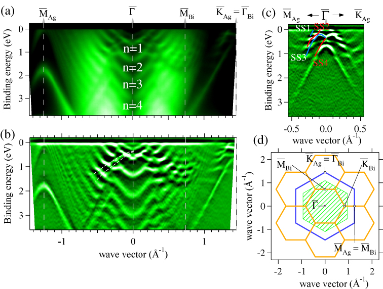
Figure 2. (a) Photoemission intensity map measured at hυ = 49.6 eV for a 15 ML Ag film grown on Si(111) 7 × 7 and covered with a  -Ag2Bi surface alloy. (b) Second derivative along the energy axis of the data displayed in panel (a). Thin dotted lines mark the position of the gaps induced by the Si band edges. (c) Same as (b) for a set of data acquired at hυ = 28.0 eV. Continuous lines identify the calculated surface states SS1–SS4 that characterize the surface alloy (derived from [45]). Blue and red colors indicate opposite spin polarizations. (d) Surface Brillouin zones of Ag film (marked by a blue line),
  -Ag2Bi alloy (marked by orange line) and Si (denoted by green shaded region). The subscript Bi refers to the alloy-related points.
Download figure:
Standard image
Figure 3. (a) The second derivative photoemission band diagram of the 15 ML-Ag(111) film prepared on Si(111) 7 × 7, measured at hυ = 49.6 eV, along the  –
– and
and  –
– directions. White arrows and red, purple and white dashed lines also indicate interaction with substrate bands.
Download figure:
Standard imageThe gaps located closer to  in figure 2(b) are ascribed to the interaction between QW states and downward dispersing surface bands, almost invisible at hυ = 49.6 eV. Figure 2(c) reports the second derivative of a photoemission map taken at lower photon energy (hυ = 28.0 eV), which brings to light the Bi-related electronic states of the system. The continuous lines drawn at negative k∥ values in this figure represent the two Rashba-split surface state pairs of the Ag2Bi alloy grown on a Ag(111) bulk crystal drawn from[45]. The obvious overlap of these lines with our experimental data, besides the distortions in the vicinity of the gaps, confirms the origin of the bands and allows us to define their spin and symmetry character [46]. Blue and red colors identify opposite spin polarizations. SS4 is an spz-type state, while SS1 derives from pxpy orbitals. SS2 and SS3, being close in energy, have mixed pxpy–spz characters [46]. As already discussed in [38], the symmetry properties of these bands define their degree of hybridization with the QW states.
The interactions of QW states with substrate and Bi-derived surface bands have a marked influence not only on the energy–momentum dispersion relations but also on the energy contours of the film electronic states. The topmost row of figure 4 reports constant energy maps for the bare Ag film taken at 0, 0.26, 0.70, 0.80, 0.90, and 1.36 eV below EF (from the first to the sixth column, respectively). According to the band structure calculations for Ag(111) film as shown in figure 1, in this wavevector range (|kx|, |ky| < 0.6 Å−1) one would expect sequences of circles centered at  . Instead, in the six panels, some film states display hexagonal-like contours, whose in-plane orientation changes with increasing the binding energy. The Shockley surface state and the n = 1 QW state, which are electronically decoupled from Si (as shown in figure 3), give rise to only circular features. The other states show hexagonal-like contours at certain binding energies. An orientation change is clearly visible by comparing the shape of the n = 2 QW state in the second and third panels, for instance.
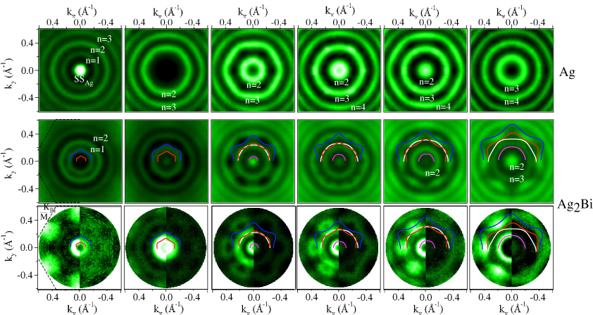
Figure 4. Constant energy photoemission maps measured at 0, 0.26, 0.70, 0.80, 0.90, and 1.36 eV below EF (from the first to the sixth column, respectively) for the bare (topmost row) and Bi-covered Ag(111) film. Photon energy is 49.6 eV for the first and second row and 28.0 eV for the bottommost row. Blue, red, white, and purple solid lines identify the SS1–SS4 surface states. These lines are traces of experimental data. The measurement geometry for the bottommost row is given in figure 5.
Download figure:
Standard imageThe behavior described above is intimately connected to the band structure of the substrate [44]. The HH and LH band edges are anisotropic and intercept a QW state at different energies as a function of the wavevector direction. This is well illustrated in figure 3 by the asymmetric gap distribution along the HH and LH edges in  –
– and
and  –
– directions. For the specific case of Ag films on elemental semiconductors, the QW state branch above an energy gap is offset to larger k∥ values with respect to the corresponding branch below the gap. Therefore, on a constant energy plane the sector of a QW contour above a gap appears to be stretched toward the surface Brillouin zone boundaries, with respect to the portion of it below the gap. Due to the crystallographic symmetry of the system, this mechanism gives rise to obvious hexagonal-like distortions, with their orientation defined by the shape of the HH and LH band edges. On the other hand, the interaction with the isotropic SO band edge, although responsible for gap openings (figure 3), does not influence the circular shape of the QW contours.
Much more complex electronic patterns characterize the Bi-terminated Ag film. The second (hυ = 49.6 eV) and third (hυ = 28.0 eV) rows of figure 4 report constant energy cuts for this system. The two halves of the photoemission maps in the bottommost row are built from data acquired under different measurement geometries (see figure 5). The difference between the right and left maps in the bottommost row is purely due to a matrix element effect [47]. Overdrawn lines mark the alloy-related surface band contours. At EF, i.e. the first column, the n = 1,2 QW states are fully decoupled from SS1 and SS2, which show up selectively in the upper and lower panels, respectively. In the next column, SS1 and the n = 1 QW state hybridize and acquire a common hexagonal-like shape, with an orientation opposite to that dictated by the HH band edge. In the third column, one can see only weak intensity modulations along the n = 3 QW state in the central row of the figure, and in the row below a hybrid contour with flower- (left-hand side) or star-like (right-hand side) shapes. Finally, in the fourth panel the hexagonal-like n = 3 QW state appears to be modulated on the inner side by a SS1-induced 12-fold pattern. SS2 and SS3 are very close in energy throughout the region considered in figure 4 and generate nearly circular contours until they meet the n = 3,4 QW states in the fifth and sixth panels. Here, the hybridization gaps along the six  –
– in-plane directions seem to break the continuity of the QW energy contours and give rise to shadow star-like patterns. SS4 shows up from the third panel onwards and negligibly modifies the shape of the QW state, as expected from the symmetry analysis reported in [23]. It is worth noting that the QW states recover their original circular shape when the interaction with the Bi-related bands ceases (n = 2,3 states in the fifth and sixth panels, second row of the figure, respectively).
The changes of surface symmetry and periodicity associated with the Ag2Bi alloy formation have a strong influence on the electronic structure of the system at large wavevectors. The original  and
and  points become
  and
and  points for the second alloy-derived surface Brillouin zone, respectively (figure 2(d)). Interestingly, not only are the surface states centered at
  replicated at
  (right-hand side of figures 2(a) and (b)), but also a new family of QW states emerges from the same point. All these states fold back at
  (k∥ = 0.627 Å−1, halfway between
  and
and  ). The SS2 state appears in figure 2(a) as a shadow parabolic band with a minimum of 1.8 eV at
  . Above it, the QW states give rise to wavy patterns that disperse upwards and symmetrically with respect to
  . This type of band was discovered in Ag films on Ge(111) [48–50] and explained in terms of interface-mediated umklapp scattering of the QW states. For the Bi/Ag/Si system similar surface-mediated scattering effects, with a characteristic reciprocal vector determined by the
  -Ag2Bi unit cell, are responsible for the electronic patterns centered at
  . Further wavy features observed in figure 3 about
  and again in figure 2(b) at the same position are obviously attributed to a Si-induced scattering effect.
We performed calculations based on the nearly free-electron (NFE) model to simulate the wavy bands measured along the  –
– –
– (
( ) line and reported in figure 6 (zoom of figure 2(b) centered at
  ). We set eight NFE states as QW subbands at
  and
and  . The energy position and effective mass of each band were chosen to fit the photoemission data at
  . The band interaction term |VAg2Bi| (off-diagonal element) was determined from the size of the experimental gap at
  (2|VAg2Bi| = 140 meV) and set to |VAg2Bi| = 70 meV. The results of the simulation, drawn as thin red lines in figure 6, show reasonable agreement with the experimental data, thus confirming the origin of the observed wavy electronic patterns.
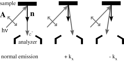
Figure 5. The geometry of the experimental set up for measuring the bottommost row data in figure 4. A is the polarization vector and n is the vector pointing to surface normal. The distinctive spectral appearance between + kx and − kx in the bottommost row in figure 4 is probably due to the photoemission matrix element effect of the measurement geometry. The angle between linear polarized light incidence and the sample normal is set to 44°.
Download figure:
Standard image
Figure 6. Zoom of the photoemission data displayed in figure 2(b) between the  and
and  points. Thin red lines are the results of a band structure simulation based on the NFE model.
Download figure:
Standard image4. Conclusion
We performed a detailed photoemission analysis of a Ag2Bi-terminated Ag quantum film on Si(111). By full two-dimensional band mapping we identified in the film electronic structure the effects of hybridization with the four surface bands and the three Si upper band edges. Multiple gaps opening along well-defined curves in the energy–momentum space alter the character of the Ag sp-derived states and give rise to complex electronic patterns. We demonstrated that the wavy bands observed at large wavevectors originate from the exchange of a surface-related reciprocal vector, in analogy to interface-mediated umklapp scattering effects in Ag/Ge or Ag/Si junctions.
Acknowledgments
This work was supported by JSPS (KAKENHI 18360018), the Italian MIUR (grant no. PRIN 20087NX9YT), and Executive Program of Cooperation in the Fields of Science & Technology between the Government of Italy and the Government of Japan for the period from 2008 to 2009. The supporting experiment at Photon Factory was performed at BL-18A with a proposal number of 2008G100.