
Abstract
DyBa2Cu3O7−x (DyBCO) films with MgO buffer layers were grown on Hastelloy substrates by inclined substrate deposition (ISD). An almost linear increase of the critical current with the DyBCO film thickness was observed. A maximum critical current of 1018 A cm−1 was measured for a DyBCO film with 5.9 μm thickness, yielding a critical current density of 1.7 MA cm−2 at 77 K and self-field. Transmission electron microscopy (TEM) yielded highly biaxially textured DyBCO films at all thicknesses and, thus, no significant decrease of the critical current density occurs with the film thickness. ISD yields a non-zero component of the growth direction parallel to the DyBCO (a, b)-plane since the DyBCO grows on a faceted MgO surface and avoids a-axis growth. Therefore, the ISD technology offers a unique possibility to overcome thickness limitations in coated conductor technology.
Export citation and abstract BibTeX RIS
1. Introduction
ReBa2Cu2O7−x (Re: rare earth) coated conductors are to date the most promising high temperature superconducting (HTS) wires for applications in energy technology [1]. They are the key device for implementing superconductivity in magnet and energy technology for reducing electrical losses. They consist of biaxially textured HTS thin films deposited on metal substrate tapes using oxide buffer layers [1]. The critical current density, jc, of coated conductors is in the range of 105–107 A cm−2 and is one key property of the superconducting material used, depending on temperature and magnetic field [2]. Critical currents are relevant for technological applications and are obtained by multiplying jc by the cross-section of the superconducting film. Note that for coated conductors the critical currents per width of the tape are specified in A cm−1. Coated conductors are being commercialized; however, their maximum critical currents are still limited to about 300–400 A cm−1 at 77 K and zero magnetic field [3].
Most of the relevant applications (motors, transformers etc) for superconducting wires are operated at a magnetic field between 2 and 6 T. In the presence of a magnetic field the critical current density of superconducting wires decreases due to flux flow [4]. Inserting nano-inclusions into the superconducting material is one possibility to pin magnetic vortices and reach higher critical current densities [5–7]. Record values of 1010 A cm−1 were reported at 75.6 K and self-field for a 2 μm thick film with BaZrO3 nano-rods and Y2O3 nano-particles [5]. For another coated conductor with nano-inclusions critical current densities were 1 × 10⁶ A cm−2 for a magnetic field of 2 T and 1.8 × 10⁵ A cm−2 for 6 T, respectively [6].
The critical current of coated conductors could be increased by increasing the thickness of the superconducting layer. However, a scale-up of the thickness is limited to about 2 μm by fundamental issues related to the thin film growth process of rolling assisted biaxially textured substrates (RABiTS) [8] and ion beam assisted deposition (IBAD) [9–12]. More recently, PLD deposited GdBa2Cu2O7−x thick films [13] and SmBa2Cu2O7−x thick films deposited by reactive co-evaporation on IBAD substrates [14] yielded critical currents up to 1000 A cm W−1. In this paper we will report results with much thicker DyBCO films grown by ISD [15].
2. Experiment
In ISD technology biaxially textured MgO buffer layers are deposited at room temperature on untextured Hastelloy tapes. MgO is evaporated by an e-gun source and the Hastelloy tape is tilted with respect to the incoming MgO flux (tilting axis parallel to width of the tape). The anisotropy of the MgO surface energy and the thermally activated directional diffusion yields the biaxial texture and a faceted surface of the MgO buffer layers [16]. For the sample studied here a 5.9 μm thick DyBCO layer was deposited at 700 °C in untilted geometry after MgO buffer layer deposition; the length of the samples was 3 cm.
The ISD MgO buffer layer was grown using standard deposition conditions in our reel-to-reel ISD system on electro-polished Hastelloy substrates. For this special experiment the substrate was not moved and we used a fixed substrate tilting angle of 36 °C. The first 400 nm of the DyBCO layer were grown under untilted conditions and at elevated temperatures with our standard setup and standard deposition conditions in the HTS reel-to-reel system [15, 17]. The deposition temperature of the DyBCO seed layer is hard to measure precisely. It is in the range between 600 and 800 °C. After this an additional layer of DyBCO was deposited in a different HTS chamber yielding a total thickness of 5.9 μm.
For measuring the critical current a 2 mm long and 1.1 mm wide bridge was etched using standard photolithography. We determined the critical current of the sample using a 1 μV mm−1 electric field criterion by a four-probe measurement. The usual 1 μV cm−1 could not be applied because the signal noise exceeded the threshold voltage of 200 nV for this criterion. However, n values [18] of these materials are about 32 [15] and thus only a small error (about 7%) is introduced with respect to the 1 μV cm−1 criterion.
Scanning electron microscope (SEM) cross-section samples were prepared by mechanical grinding and polishing. SEM images were acquired with a JEOL 6500F SEM equipped with a backscattered electron (BSE) detector. TEM samples were prepared in cross-section by the focused ion beam (FIB) method using a Zeiss AURIGA®-CrossBeam® workstation. A thin TEM lamella was cut out by the ion beam, lifted out, and finally attached to a TEM grid. For image acquisition in the TEM, samples were oriented such that the c-axis of the DyBCO was lying in the image plane, i.e. the MgO/DyBCO interfaces were parallel to the electron beam.
Images and diffraction patterns were acquired in a Zeiss EM912Ω operated at 120 kV using a 5 or 10 eV energy slit aperture of the Omega energy filter to reduce inelastically scattered electrons contributing to the image background. Diffraction patterns were acquired with a 700 nm selected area aperture. The MgO/DyBCO interface roughness was measured from SEM cross sectional images and the DyBCO surface roughness was measured from TEM cross sectional images.
3. Results
A record critical current of 112 A or 1018 A cm−1 was measured at 77 K and self-field for the bridge. As the thickness of the superconducting layer was 5.9 μm, this corresponds to a critical current density of 1.7 MA cm−2.
Several coated conductors with increasing film thickness were measured in this way. Figure 1 shows the critical current measured as function of the DyBCO film thickness. An almost linear increase of the critical current with film thickness was observed up to 7.5 μm. The critical current density of DyBCO films with a thickness of 6 μm is close to that of thinner DyBCO films (DyBCO thicknesses up to 2 μm), for which jc ranges from 1.6 to 2.6 MA cm−2. This indicates the critical current density does not decrease significantly with thickness. A detailed analysis of the microstructure of such coated conductors was carried out for understanding the growth mechanism.

Figure 1. Critical current per centimeter tape width versus DyBCO film thickness of ISD coated conductors. The red asterisk indicates the sample investigated by SEM and TEM.
Download figure:
Standard imageFigure 2(a) shows a secondary electron image of the MgO surface in plan view after the ISD deposition of MgO and prior to the deposition of the DyBCO film. The MgO surface consists of sharp and flat facets about 230 nm in size arranged in a tile-like structure; the edges of the facets appear in bright contrast. The facets were found to be parallel to (002) planes of the MgO and their surface normal is almost parallel to the direction of the incoming vapor during ISD deposition. Figure 2(b) shows a BSE image of the layer structure in cross-section after the DyBCO deposition. The MgO layer thickness and the DyBCO film thickness were 2.25 μm and 5.9 μm, respectively. The areas of different contrast are secondary phases, namely copper oxides (dark) and dysprosium oxides (bright). These secondary phases appear due to Ba deficient powder used for the DyBCO growth. An enlarged view of the MgO/DyBCO interface is shown in the inset in figure 2(b); some edges of the MgO facets are marked by black arrows. The DyBCO surface had a roughness of less than 200 nm measured over a length of 12 μm of the film. XRD data documenting the biaxial texture of both the ISD and the DyBCO layer are presented elsewhere [17].

Figure 2. (a) Plan view image of MgO facets prior to DyBCO deposition. (b) Backscattered electron image of the layer structure of a fully processed sample in cross sectional view. In the inset arrows are pointing to the MgO facets. (c) Schematic image showing the facets at the MgO/DyBCO interface.
Download figure:
Standard imageA schematic drawing of the MgO/DyBCO interface is shown in figure 2(c) based on our results of a large number of cross-sections investigated by TEM [19]. The growth directions as well as the crystallographic axes of the DyBCO film are indicated. The (001) direction of DyBCO encloses an angle of 24° with the substrate normal. As a consequence, the growth direction has a non-zero component parallel to the crystallographic (a, b)-plane of the DyBCO for the ISD geometry. Note that the DyBCO (a, b)-plane is parallel to the MgO(200) plane. In figure 2(b) arrows point to edges of facets from which grain boundaries emerge into the DyBCO film. The grain size in the lower part of the DyBCO film correlates with the facet size (230 nm). Grain boundaries are tilted with respect to the substrate normal in a direction opposite to the (001) direction of DyBCO.
Figure 3 shows a low-magnification TEM bright-field image of the top part of the DyBCO layer in cross-section. A DyBCO grain size of 500–600 nm was measured in the upper part of the DyBCO film and a DyBCO surface roughness of 140 nm was determined. Therefore, we observed an increase of the DyBCO grain size with increasing film thickness. The orientation of the DyBCO c-axis was found to be fixed throughout the film thickness. The diffraction pattern is shown in false color to highlight the splitting of reflections due to DyBCO small-angle grain boundaries. The small inset in figure 3(a) shows three DyBCO(00l) reflections separated by a maximum angle of 4°. Therefore, the DyBCO grains of the investigated area are separated only by small-angle grain boundaries; this was found to be true for all analyzed areas.
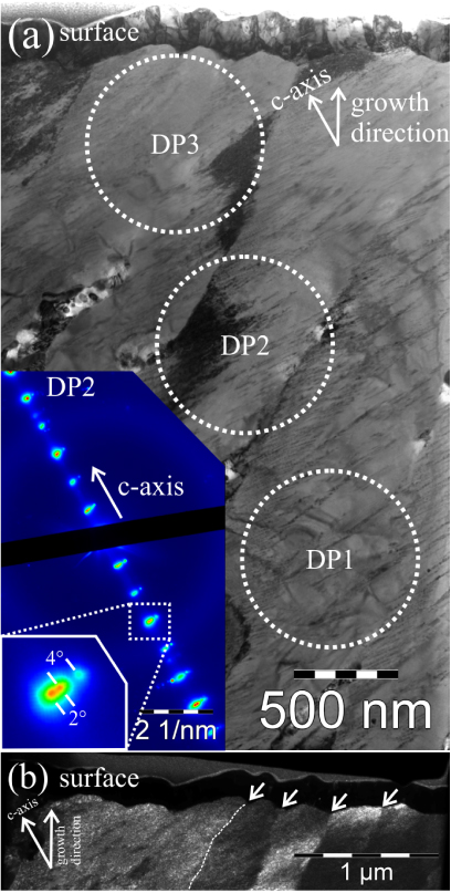
Figure 3. (a) Cross sectional TEM bright-field image of the top 3 μm of a 5.9 μm thick DyBCO film. The inset displays the diffraction pattern DP2 in false color. Diffraction patterns DP1 and DP3 are not shown here. The white circles mark the size of the selected area aperture used for acquiring diffraction patterns. (b) TEM (002) dark-field image of the topmost part of (a). The white arrows indicate DyBCO grain boundaries.
Download figure:
Standard imageFigure 3(b) shows a (002) dark-field image of the top part of the DyBCO film close to the surface; grain boundaries are marked by white arrows. Consistent with the schematic drawing (figure 2(c)) the DyBCO grain boundaries (figure 3(b)) were found to be tilted with respect to the substrate normal opposite to the (001) direction.
4. Discussion
In this paper it was shown that ISD technology offers unique possibilities to grow monolithic thick films, exceeding 2 μm in thickness. In ISD technology sharp and well defined MgO(002) facets [20] (their width is about 230 nm) provide a tilted (about 25°) surface for the growth of the superconducting layer. Despite the large lattice misfit (8.5% between MgO and DyBCO), the DyBCO film grows epitaxially on top of the MgO buffer layer, i.e. the (hk0) directions of MgO are parallel to the (hk0) directions of the DyBCO. The DyBCO(001) direction was found to be always parallel to the MgO(002) direction. As a consequence ISD deposited DyBCO films have a non-zero component of the growth direction parallel to the (a, b)-plane of the DyBCO grains, as shown in figure 2(c). This makes the c-axis growth very stable, suppressing a-axis growth and yields a perfect transfer of the biaxial texture of the MgO buffer layer into the DyBCO layer. a-axis grains would form large-angle grain boundaries and, therefore, would dramatically reduce the critical current density within the tape [21]. In contrast, the growth direction does not have a component parallel to the (a, b)-plane of YBa2Cu3O7−x (YBCO) for the RABiTS and IBAD growth process. As a consequence, thick films grown by these technologies show a-axis growth and porosity (dead layer effect) [8, 12, 22, 23]. Coated conductors fabricated by the RABiTS and IBAD technology can carry the same amount of critical current; however, a more complicated architecture in the superconducting layer is required, yielding an increase in processing cost and time.
For ISD technology, the individual grains retained their biaxial texture over the total film thickness (5.9 μm, figure 3) and neither porosity nor a-axis growth was observed. Critical currents exceeded 1000 A cm−1 at a temperature of 77 K and self-field.
5. Conclusions
In summary, ISD technology yields significant advantages since (i) DyBCO films can be grown as monolithic thin films avoiding a-axis growth and (ii) it yields larger critical currents as compared to IBAD and RABiTS for monolithic films. ISD yields highly biaxially textured DyBCO films at all thicknesses and no significant decrease of the critical current density with film thickness. This is due to the growth process on a faceted MgO surface yielding a non-zero component of the growth direction parallel to the (a, b)-plane of the DyBCO. A maximum critical current of 1018 A cm−1 was measured for a DyBCO film with 5.9 μm thickness, showing that in ISD technology critical transport currents exceeding 1000 A cm−1 can be realized by simply increasing the HTS film thickness.
Acknowledgments
The authors would like to thank the NMI Reutlingen for FIB sample preparation and acknowledge financial support from the Bundesministerium für Wirtschaft und Technologie (BMWi), project HIGHWAY, FK 0327489C.