
Abstract
Monolithic scintillator detectors can offer a combination of spatial resolution, energy resolution, timing performance, depth-of-interaction information, and detection efficiency that make this type of detector a promising candidate for application in clinical, time-of-flight (TOF) positron emission tomography (PET). In such detectors the scintillation light is distributed over a relatively large number of photosensor pixels and the light intensity per pixel can be relatively low. Therefore, monolithic scintillator detectors are expected to benefit from the low readout noise offered by a novel photosensor called the digital silicon photomultiplier (dSiPM). Here, we present a first experimental characterization of a TOF PET detector comprising a 24 × 24 × 10 mm3 LSO:Ce,0.2%Ca scintillator read out by a dSiPM array (DPC-6400–44–22) developed by Philips Digital Photon Counting. A spatial resolution of ∼1 mm full-width-at-half-maximum (FWHM) averaged over the entire crystal was obtained (varying from just below 1 mm FWHM in the detector center to ∼1.2 mm FWHM close to the edges). Furthermore, the bias in the position estimation at the crystal edges that is typically found in monolithic scintillators is well below 1 mm even in the corners of the crystal.
Export citation and abstract BibTeX RIS
For more information on this article, see medicalphysicsweb.org
1. Introduction
Detectors for time-of-flight (TOF) positron emission tomography (PET) are required to exhibit high γ-photon detection efficiency (γ-PDE), good energy resolution, good spatial resolution, and excellent timing resolution. Preferably, they should also provide depth-of-interaction (DOI) information. In order to simultaneously optimize these key properties, certain trade-offs need to be made in the design of conventional (TOF) PET detectors that utilize pixelated scintillators. For example time resolution, energy resolution, and detection efficiency may need to be sacrificed to obtain the best possible spatial resolution in the design of detectors for preclinical scanners (Miyaoka et al 2001, Yang et al 2004). Detectors for application in whole-body clinical PET systems, on the other hand, are usually optimized for detection efficiency, time resolution, and energy resolution, at the expense of spatial resolution (Surti et al 2007, Lois et al 2010, Jakoby et al 2009). Detectors that utilize monolithic scintillators on multi-channel light sensors are capable of high spatial resolution without compromising on the energy performance (Bruyndonckx et al 2004, 2008, Maas et al 2006, van der Laan et al 2007, Schaart et al 2009, Llosá et al 2010, van Dam et al 2011a, de Acilu et al 2012, Sarasola et al 2011, Miyaoka et al 2008). Moreover, monolithic scintillator detectors intrinsically provide DOI information (van Dam et al 2011b, Carles et al 2012), are relatively uncomplicated to assemble, and can offer an excellent coincidence resolving time (Seifert et al 2012a, van Dam et al 2013). Perhaps the most important drawbacks of the monolithic scintillator concept are the need for dedicated calibration procedures and the relatively large number of data channels that need to be handled. Both issues, however, appear to be solvable with modern readout and processing electronics. For example, the number of data that needs to be transferred can be reduced drastically by on-line FPGA processing, while methods for efficient calibration are under development (van Dam et al 2011a, Li et al 2010, Miyaoka et al 2010).
In monolithic scintillator detectors the interaction points of γ-photons within the scintillator are estimated on the basis of the measured light distributions. Among other things, the accuracy of this estimate depends on the signal-to-noise ratio per sensor channel. The signal amplitudes per channel can be relatively low for monolithic scintillator detectors as the scintillation photons are distributed over all sensor pixels. It is therefore imperative for the performance of these detectors that the overall readout noise (including electronic noise, dark noise, and multiplication noise) is kept as low as possible.
A new type of photosensor that is very interesting in this respect is the so-called digital silicon photomultiplier (dSiPM). This device offers negligible electronic noise, low photon-signal transit time spread, and a PDE that is comparable to state-of-the-art photomultiplier tubes or analogue SiPMs (Frach et al 2009).
Similar to analogue SiPMs, dSiPMs are composed of a large number of single-photon avalanche photodiodes (SPADs), yet with active quenching as opposed to passive, resistive quenching. This facilitates the digitization of the signals of individual SPADs (triggered by individual scintillation photons), practically eliminating all electronic readout noise. Furthermore, the SPADs are kept inactive once they have triggered, until a global reset is issued. As a result, dSiPMs suffer neither from the contributions of afterpulsing, nor from the triggering of partially recharged SPADs, greatly reducing the multiplication noise. The fact that this comes at the cost of decreased dynamic range is of little or no consequence for the readout of monolithic scintillators, because of the relatively low number of scintillation photons impinging on each sensor pixel. Lastly, it has been demonstrated that dSiPM (arrays) are capable of outstanding timing performance (Degenhardt et al 2009, van Dam et al 2013).
In summary, dSiPMs would appear to be highly suited for application in monolithic scintillator detectors for TOF PET. In this work we present an initial characterization of a detector comprised of a 24 mm × 24 mm × 10 mm 0.2%Ca codoped LSO:Ce crystal read out by 6 × 6 pixels of a prototype 8 × 8 dSiPM array.
2. Methods
2.1. Materials
2.1.1. Digital silicon photomultiplier array
The detector characterized in this work is read out by a prototype array of dSiPMs (DPC-6400–44–22 from Philips Digital Photon Counting, see Frach et al (2009) and Degenhardt et al (2009)).
As dSiPMs are a relatively novel type of photosensor we briefly review their most important features. We emphasize that some details of the functionality and readout architecture of the DPC-6400–44–22 prototype sensor array may be subject to change in later versions, such as the DPC-3200–44–22 array that recently became available. For a proper understanding of its operation it is important to define some terminology regarding the different levels of subdivision of a dSiPM array. This subdivision is illustrated in figure 1. The DPC-6400–44–22 dSiPM array is composed of 4 × 4 individual silicon dies. On each die, four dSiPM pixels are arranged in a 2 × 2 matrix. This grouping of pixels onto the dies is important in so far as pixels that belong to the same die share a common controller and time-to-digital converter (TDC), i.e. a single timestamp is obtained per die for each event. Each pixel comprises 6396 so-called microcells arranged into 64 rows and 100 columns (with 4 cells missing in the center of the pixel). For the purpose of trigger handling, the pixels are furthermore subdivided into quadrants, each of which comprises 1599 microcells arranged in 32 rows and 50 columns. These four pixel quadrants are referred to as subpixels.

Figure 1. Schematic representation of the digital silicon photomultiplier (dSiPM) array. The larger inset depicts a zoom on a single die consisting of four pixels. Each pixel contains 6396 microcells (a number of which are shown in the smaller inset) that are arranged into 4 subpixels.
Download figure:
Standard imageEach microcell comprises a SPAD and additional control circuitry in 180 nm CMOS technology. This control circuitry facilitates active quenching of the SPAD after breakdown. Similar to analogue SiPMs the breakdown of a SPAD can occur due to either photon-generated or thermally generated charge carriers. The latter type of discharge is commonly referred to as a dark count. The microcell control circuitry includes functionality for active recharging of the diodes as well as selective enabling/disabling of individual cells.
The cell control units furthermore provide a fast trigger signal when a discharge is initiated in one of the SPADs, which is sent to a balanced trigger network. The trigger signals of all cells that belong to a given subpixel are combined to create a subpixel trigger (ST); i.e. the ST corresponds to the trigger signal of the first microcell that is triggered on the subpixel. A master trigger (MT) for the entire pixel is created from its four ST signals following a programmable set of logic operations. For the DPC-6400–44–22 these are (Frach et al 2009):
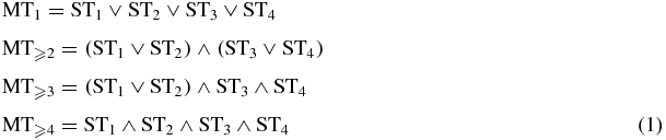
where STn = ST1 ... ST4 are the trigger signals obtained from the different subpixels.
The simplest case, MT1, corresponds to the OR of all STn and the MT is associated with the first triggered microcell on the pixel. In this work MT⩾2 is employed as this reduces the rate of dark count related triggers. It should be noted, however, that in general the MT1 trigger produces more accurate time stamps. The definition of MT⩾2 requires that at least two cells are triggered: one cell on each pixel half. More fired cells are required if the first two (or more) cells are triggered on the same pixel half. A generated MT is sent to a die controller which is shared by the four pixels on the die. When the die controller receives a MT, two integrated TDCs are started. These 9 bit TDCs are stopped by 100 MHz reference signals with a respective phase shift of 180°. These reference signals are derived from a 200 MHz system clock that synchronizes all dies.
When a MT is received, the die controller enters the so-called validation phase. After a configurable validation time (here set to 4 clock cycles corresponding to 20 ns with an additional offset of 5–10 ns) each of the four pixels on the die is checked for a validation condition that can be set by the user. In this work the validation condition is set such that each corresponding subpixel must contain at least one triggered microcell. It is important to note that neighbor logic between dies was not yet implemented in the DPC-6400–44–22 prototype dSiPM array. Hence, all dies covered by the monolithic scintillator need to be validated independently for the complete readout of a scintillation event.
In the case that no pixel of a triggered die meets the validation condition, a fast reset is performed, i.e. all microcells are recharged and the TDC is reset. The time required for this reset is configurable. Here it is set to 15 ns as a compromise between reset speed and the maximum of the required supply current during the reset. The resulting dead time (validation time + reset time) for each non-validated trigger event thus is ∼40 ns in this work. If at least one of the pixels is validated, the die enters the integration phase in which the pixels remain active throughout an adjustable time window (here set to 165 ns). Then, in the readout phase (taking 680 ns) a row-by-row cell count is performed during which the cells that are not read out can still detect photons. This is followed by a reset. The cell count of each pixel is stored on the die memory which can hold up to 28 events. The readout of the dies is frame-based with a frame length of 330 µs.
2.1.2. Detector assembly
The detector under test comprises a monolithic, 0.2%Ca codoped LSO:Ce scintillator supplied by Agile Technologies, Knoxville, TN, USA. The crystal has dimensions of 24 mm × 24 mm × 10 mm and all of its surfaces are polished. The 24 mm × 24 mm base surface of the crystal was optically coupled to an area comprising 6 × 6 pixels (i.e. 3 × 3 dies; see also figure 2) on the dSiPM array, using Cargile Meltmount 1.582. The crystal was wrapped in Teflon tape to maximize the light collection on the sensor array. Additionally, a coincidence detector was assembled in the same manner, comprising a 10 mm × 10 mm × 20 mm monolithic LYSO:Ce crystal and a second dSiPM array, with one 10 mm × 10 mm crystal surface centered on one die of the array.
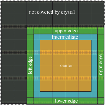
Figure 2. In scale representation of the dSiPM array depicting the area covered by the scintillation crystal and the selected regions of interest used in the analysis of the data.
Download figure:
Standard image2.1.3. Paired collimator setup
The paired-collimator setup schematically shown in figure 3 was employed to facilitate the irradiation of the detector at well-defined positions with 511 keV annihilation photons. The paired-collimator housing is designed such that it encloses a  0.5 mm22Na source (7.4 MBq) on all sides with >3 cm tungsten. The position of the source within the housing can be adjusted by two positioning screws for alignment. The γ-photon beam is defined by the 0.5 mm aperture of the 80 mm thick tungsten collimator facing the detector under test. The alignment of the 22Na source with this front side collimator was performed by maximizing the count rate measured at the collimator exit. A
  5 mm bore in the housing opposing the front side collimator with an exchangeable lead collimator attachment (here 25 mm thick with a
  5 mm aperture) allows to measure annihilation photon pairs in coincidence.
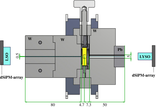
Figure 3. Drawing of the paired-collimator setup. A  0.5 mm 22Na source is positioned between two collimators: a
  0.5 mm × 80 mm collimator that defines the beam on the detector under test and a
  5 mm × 50 mm collimator on the backside that allows measuring pairs of 511 keV annihilation photons in coincidence. All dimensions in the figure are given in units of millimeters.
Download figure:
Standard imageThe detector under test is mounted on x, y-translation stages (Physics Instruments M-304.42S). These stages have a range of 100 mm and allow the detector to be stepped though a plane perpendicular to the beam with <10 µm precision. The entire setup is placed in a light-tight, temperature-controlled cabinet (Weiss WT 450/70) to allow for accurate control of the ambient temperature which was set to 0 ± 1°C during all measurements. Operation in a low temperature environment was chosen to reduce the dark count rate (DCR) and the associated dead time (see section 2.1.1). The DCR approximately halves per every 10 °C temperature decrease.
2.2. Measurements and data processing
Prior to detector assembly the DCR for each individual microcell was recorded as described by Frach et al (2009). During all subsequent experiments the 5% of microcells that showed the highest DCRs were disabled on each die to further reduce the DCR. The summed DCR from of the remaining SPADs was 69 kHz per die (compared to from 1.85 MHz when all SPADs are included). The influence of the DCR on the energy and spatial resolution is thus expected to be negligible. However, a low DCR is of importance as the dead times due to validation and reset (see section 2.1.1) may render individual dies inactive during a scintillation event that is recorded by the remaining dies.
The assembled detector under test was irradiated with a beam of 511 keV annihilation photons at an equidistant 93 × 93 grid of reference beam positions (xi, yj), covering an area of 23 mm× 23 mm at a pitch of 0.25 mm. Coincidence events were recorded for 50 s (i.e. 1.5 × 10⁵ frames) at each grid position.
Only those scintillation events were accepted for further processing for which at least eight of the nine dies that are covered by the crystal were read out. This corresponds to 85% of the events recorded with an energy above ∼450 keV. As discussed above, a portion of the events for which not all dies are read out can be attributed to dark-count induced dead time. In addition, the present version of the dSiPM array does not offer neighbor logic in between dies, i.e. all dies covered by the scintillator need to be validated independently for complete read out. Yet, as the scintillation light is spread over nine dies, the light level on a given die may not be high enough to fulfil the validation condition on any of the pixels of a given die and in some cases one or more dies may not be read out. This issue may be solved in future versions of the device by the introduction of neighbor logic.
Dies that are not validated for a given event are ignored in the position estimation, which will be described below. However, a correction on the total number of registered photons is performed when estimating the energy of the γ-event. To this end, for each event in the set of measurements for which information from all nine dies is available, the ratio R between the sum of the number of fired cells of the pixels belonging to a given die, Ndie pixel, and the scaled sum of the number of fired cells recorded by the corresponding neighboring pixels, Nneighbor pixel, is determined:

where nneighbors is the number of pixels that are of direct neighbors to the corresponding die: 4 in case of a corner die, 6 for a die in the center of either edge and 8 for the die in the detector center as indicated in figure 4. Subsequently, the data is grouped according to the irradiation positions into a course grid with 2 mm × 2 mm large bins and the average Rdie is determined for each course grid bin and for each die. Lastly, the intensity of non-validated dies is estimated based on the (scaled) summed intensity of the corresponding neighboring pixels multiplied by the previously determined average ratio for the corresponding course grid position.

Figure 4. Pixels utilized to estimate the number of fired SPADs of missing corner dies (a), edge-center dies (b), and the center die (c).
Download figure:
Standard imageSubsequently, an energy window is applied to the data rejecting all events below 450 keV and above 570 keV, corresponding to the full-width-at-tenth-maximum (FWTM) of the 511 keV photopeak. Lastly, the number of events per position was trimmed by rejecting randomly selected data such that all reference beam positions contained the same number of events (n = 99).
For the position of interaction estimation all light patterns were normalized to the corresponding sum of all 36 dSiPM signals. The so-prepared set of 856 251 measured events served both as reference data for the position estimation and as test data for the determination of the spatial resolution, using the leave-one-out method described by Maas et al (2009). In short, one event in the data set was treated as unclassified, i.e. it is not assigned to any of the reference positions (classes) and removed from the reference data set. Its position was estimated with the so-called smoothed k-nearest neighbor (k-NN) algorithm described by van Dam et al (2011a). This was repeated for each event in the data set.
The smoothed k-NN algorithm assigns coordinate estimates to unclassified events in four steps.
- (1)The Euclidean distances, i.e. the square roots of the sum-of-squared-differences, of the light distribution of the unclassified event to the light distributions of all events in the reference set are calculated.
- (2)A subset of the reference data consisting of the k (here k = 100) closest matches (nearest neighbors) was selected and a histogram of their (x, y) irradiation coordinates was created.
- (3)This 2D irradiation position histogram is smoothed with a moving average filter of 5 × 5 bins. Thus, each new bin value is based on the average of 25 bin values of the original histogram. Near the edges of the histogram the number of bins for averaging was decreased at the side(s) of the edge. E.g., the averaging grid is reduced to 3 × 5 bins for bins closest to one of the edges or 3 × 3 bins for bins in the exact corner of the crystal.
- (4)The coordinate corresponding to the maximum value of the smoothed histogram was assigned as the coordinate estimate
 to the unclassified event.

A 2D-error histogram was subsequently created from the differences between all estimated coordinates and their respective 'true' irradiation points. By proper normalization one then obtains the so-called point-spread function (PSF) of the detector, assuming that the influence of the annihilation beam is negligible. The PSF was interpolated with a 2D cubic spline and the full-width-at-half-maximum (FWHM) and the FWTM of the cross-sections of the interpolated PSF were determined as measures of the detector spatial resolution along the x- and y-directions, respectively.
It has been observed in previous measurements with monolithic scintillation crystals that the spatial resolution can vary significantly as a function of the interaction position (Maas et al 2009, Bruyndonckx et al 2008, Seifert et al 2012a, Sarasola et al 2011). In order to investigate this dependency, six regions were defined according to their relative position with respect to the crystal edges as depicted in figure 2: a center region, four edge regions, and an intermediate region. The center region is demarcated by a 16 mm × 16 mm rectangle in the center of the sensor. The edge regions include all irradiation points recorded within 2 mm of either edge of the sensor. These regions will be denoted as upper, lower, left, and right edge region according to their position relative to the center region. All remaining data are collected in the intermediate region. The PSF was constructed for each of these regions as described above.
To evaluate a possible bias in the position estimation a bias vector b(v) was calculated at each reference beam position v = (xi, yj), in the same way as described by Seifert et al (2012a):
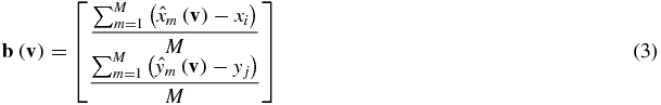
where  and
and  are the estimated x, y-coordinates of the mth data point recorded at v. M is the number of reference events per position (viz M = 99). As pointed out in Seifert et al (2012a) it may be important to exclude possible contributions of random and scattered events. Thus only those terms were taken into account in the corresponding sums in (3) for which
  and
and  are smaller than 3 mm (corresponding to approximately the FWTM of the PSF, see section 3.2.1). It is emphasized, that his selection criterion in only applied in the determination of the bias of the position estimation. The determination of the PSF and the corresponding FWHM/FWTM values was performed using the entire data set.
3. Results and discussion
3.1. Energy spectra
Figure 5 depicts two photon-count histograms for events for which exactly eight dies were recorded: one showing the data as measured and the other the data with each event corrected for the expected number of fired SPADs on the missing die (as described in section 2.2). This correction process assigns on average 90 fired SPADs to the missing die. These spectra are compared to the spectrum containing only events for which all nine dies were recorded. The difference between the photo peak position in this '9-dies-spectrum' and the photo peak position in the 'corrected 8-dies-spectrum' is ∼0.25% only. However, the comparison of the two spectra seems to indicate a small bias of the missing-die-value estimation toward slightly larger values. We explain this by the fact that in the majority of the cases a die was missing because it failed the validation criterion. This is most probable at very low photon count. The condition that one die is missing in a given event is thus biased towards events for which one die receives an unusually small number of photons. The assignment of an average value to the missing die then causes the observed bias.
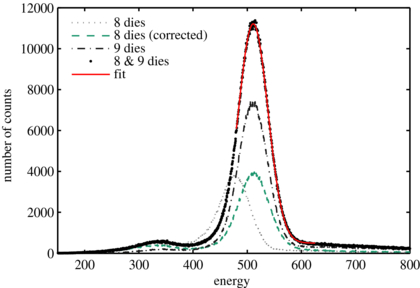
Figure 5. Energy spectrum recorded with a 22Na source. The spectrum is depicted together with the corresponding Gaussian fit through the full energy peak. The FWHM of the fitted Gaussian function is equal to 12.8%.
Download figure:
Standard imageLastly, figure 5 shows the energy spectrum combining all data of events for which at least eight of the nine dies were read out. This spectrum is depicted together with a Gaussian function (red line) that was fitted to the 511 keV photopeak in the region between 485 and 630 keV. The FWHM of this Gaussian function equals 12.8%. For events within the FWTM of the photopeak, the number of fired cells on the pixel receiving the highest intensity is on average ∼130 with a maximum of ∼500. As the total number of microcells is 6396 per pixel the influence of optical SiPM saturation on the energy spectrum is considered to be negligible. The total number of fired cells is in the order of 1100 for events in the 511 keV photopeak.
The roll-off at ∼300 keV is a consequence of the condition that at least eight dies must be read out in order for an event to be accepted. At energies lower than 300 keV the (average) number of photons on the dies that receive the lowest intensity becomes so low, that the probability that at least eight dies are validated for read out becomes very small. It should be noted, that the resulting reduction of count rate influences the spectrum at energies up to ∼400 keV.
3.2. Position estimation
3.2.1. PSF and spatial resolution
Figure 6 shows the PSFs obtained in the center region, the intermediate region, the left edge region, and the lower edge region (as defined in section 2.2). The PSF for the right edge region and the upper edge region are not shown as they are essentially mirror images of the left edge region and the lower edge region, respectively. The contour lines in the plots represent the one-half and the one-tenth of the maximum values of the corresponding PSFs. The spatial resolutions in terms of the FWHM and the FWTM of the cross sections through the PSFs in the x- and in y-direction are summarized in table 1. Here we would like to point out that these values are not corrected for the finite width of the annihilation photon beam.

Figure 6. Point spread functions averaged for all irradiation positions within different detector regions as defined in figure 2: center region (top left), the intermediate region (top right), the left edge region (lower left), and the lower edge region (lower right). The contours correspond to one-half and one-tenth of the maximum value of the corresponding distribution.
Download figure:
Standard imageTable 1. Spatial resolution values for the entire detector and the different regions of interest.
| x-direction | y-direction | |||
|---|---|---|---|---|
| Region | FWHM (mm) | FWTM (mm) | FWHM (mm) | FWTM (mm) |
| Entire detector | 1.00 | 2.34 | 0.99 | 2.24 |
| Center | 0.97 | 2.01 | 0.95 | 1.94 |
| Intermediate | 1.06 | 2.39 | 1.07 | 2.43 |
| Upper edge | 0.96 | 2.30 | 1.20 | 3.39 |
| Lower edge | 0.97 | 2.31 | 1.02 | 3.01 |
| Left edge | 1.13 | 3.23 | 0.99 | 2.19 |
| Right edge | 1.28 | 3.49 | 0.99 | 2.17 |
The detector under test exhibits an outstanding spatial resolution of 1 mm FWHM averaged over the entire detector area and just below 1 mm FWHM in both the x- and y-direction in the 16 mm × 16 mm center region. It should be noted that all measurements were performed at perpendicular incidence in this initial test of the dSiPM-based monolithic scintillator detector. Reconstructing the interaction positions of γ-photons that enter the crystal under oblique angles in principle is not problematic, as the light distributions carry intrinsic information on the DOI (Bruyndonckx et al 2004, Maas et al 2009, Schaart et al 2009).
The resolution appears to worsen slightly to about 1.2 mm FWHM for interaction positions in the vicinity of the edges. It is interesting to note that this degradation is limited to the direction perpendicular to the closest edge, i.e. the width of the PSF remains unchanged in the x-direction for events close to the upper and lower edge, whereas the distance to the left and right edge does not influence the resolution in the y-direction. We observed the same effect in previous works with different sensors and different monolithic scintillators (Schaart et al 2009, Seifert et al 2012a, Maas et al 2009). The reason as to why the width of the PSF increases toward the edges might be found in the fact that the (expected) change of the light distribution with a given change in the interaction position becomes smaller as one of the edges is approached.
The degradation of the spatial resolution appears to be significantly stronger close to the upper edge and the right edge than near the lower edge and the left edge, respectively. The reason for this remains unclear. However, it might be an indicator of a misalignment of the crystal.
Furthermore, it is to be noted that the fraction of events for which only 8 dies were validated is 38%. It thus appears that the position estimation algorithm is remarkably robust with respect to the missing information of one die. This is congruent with the abovementioned fact that in many cases a die is not validated because the number of photons impinging on it is too small to fulfil the validation criterion, which implies that little information regarding the γ-interaction position is lost.
3.2.2. Positioning bias
The variation of the magnitude and direction of the calculated bias vector b(v) with the reference beam position v is illustrated in figure 7. For clarity, the average of b(v) over intervals of 3 × 3 irradiation positions (i.e. 0.75 mm × 0.75 mm) is displayed. The color scale indicates the absolute length of b(v), calculated as the Euclidian norm of b(v). The basic features that can be identified in this image are very similar to those observed previously with a detector employing a monolithic LaBr3:5%Ce scintillator and an (analogue) SiPM-array (Seifert et al 2012a): the magnitude of the bias is negligible in the detector center (<0.1 mm), while the bias in the intermediate region is pointed toward the closest edge(s) of the detector and the bias in the edge region is directed towards the crystal center.
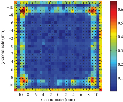
Figure 7. Bias vector b(v) averaged over 3 × 3 irradiation positions (0.75 mm × 0.75 mm) as a function of the (average) reference beam position v. The color scale indicates the length of b(v).
Download figure:
Standard imageNevertheless, the magnitude of the observed bias is significantly smaller for the present detector than for the one reported on previously (Seifert et al 2012a). It can be observed in figure 7 that the bias remains well below 1 mm even in the worst case (i.e. close to the corners of the crystal), whereas a bias of up to 1.5 mm was observed for the LaBr3:5%Ce-SiPM detector. This reduction of the bias in the position estimation may be a consequence of the improved spatial resolution for the LSO-dSiPM detector compared to the previous detector. Indeed, a more detailed comparison between the bias maps for the different detectors indicates that the largest improvement of the positioning bias can be observed in the edge regions. In our earlier work we argued that the bias in this region is a consequence of the cut-off of the PSF at the edges of the detector (Seifert et al 2012a). Consequently, the range of this effect and its magnitude are related to the width of the PSF and hence the spatial resolution.
4. Conclusions
The results presented in this work show that high spatial resolution can be achieved with monolithic scintillator detectors based on dSiPM arrays. For a 24 mm × 24 mm × 10 mm LSO:Ce,Ca crystal, a spatial resolution of just below 1 mm FWHM in the center was obtained, deteriorating only slightly to ∼1.2 mm FWHM close to the edges. In addition, the bias of the positioning algorithm close to the detector edges, which is in part determined by the detector spatial resolution, is <1 mm even in extreme cases (i.e. in the corners of the crystal).
A further benefit of the dSiPM is that it offers very good single photon timing resolution, which is independent of the photosensor area and can therefore easily be maintained over the entire area of a dSiPM array. This is an essential requirement for accurate timing with monolithic scintillator detectors, since it allows spreading of the scintillation light over multiple dSiPM pixels without degrading the timing performance. In fact, obtaining time stamps from multiple photosensor pixels is beneficial as long as the contribution of electronic noise to the single photon timing jitter is negligible. This does not only follow from theory (Seifert et al 2012b) but has indeed been observed experimentally with the type of detector presented here. That is, coincidence resolving times of ∼160 to ∼180 ps FWHM have already been demonstrated, be it with a newer version of the dSiPM array (van Dam et al 2013).
It should be noted that the dSiPM array that has been used in this proof-of-concept work is a prototype and that a number of issues still need to be addressed. One area of concern, particularly for the application in monolithic scintillator detectors, is the matter of missing information from dies that do not meet the trigger criterion during a given event. This may be solved in the next generation of these arrays by a new implementation of the trigger logic and the possibility to force the validation of all silicon dies in a certain group (up to the entire array) as soon as the trigger criterion is matched for one die in the group. Such neighbor logic does not account for the issue of dies that are occupied ('dead') while processing dark counts, which would require a reduced DCR, reduced die reset and readout times, and/or the use of a MT level higher than the level MT2 used in this work (see section 2.1.1). In this respect it also needs to be investigated to which extent the operation of the sensor at higher temperatures would increase the fraction of missing dies.
Nevertheless, the initial work presented here seems to indicate that the estimation of the interaction position may be fairly robust with respect to the number of dies that are read out per event. This will be an important topic for further, more elaborate investigations on the dSiPM-based monolithic scintillator detector.
Acknowledgments
We would like to thank Carsten Degenhardt, Thomas Frach, Ralf Schulze, and Andreas Thon from Philips Digital Photon Counting for their assistance concerning the operation of the dSiPM arrays. This work is partially funded by EU FP7 project SUBLIMA, grant agreement no 241711, see also www.sublima-pet-mr.eu.