
Export citation and abstract BibTeX RIS
In 1948, A new microscopic principle was proposed by Gabor [1] to correct the electron micrographs by measuring the electron beam phase shift induced by the aberrations of the electron optic and compensate for them. He called this technique 'holography' from the Greek 'holos' meaning 'whole' and 'grafe' meaning 'writing' as the method allows retrieving both the amplitude and the phase of the electron wave and not only its intensity. Gabor was awarded the Nobel Prize in Physics in 1971 for this invention. This powerful interferometric technique consists of overlapping a high energy electron wave that has interacted with a material and the possible stray fields surrounding it (the 'specimen wave'), and a wave issuing from the same electron source that has passed through the vacuum, which is the so-called 'reference wave'. For sufficiently coherent electron sources, the overlap of these two beams results in an interference fringes pattern (the hologram) superimposed on the image of the object as schematized in figure 1. The relative phase shift between the specimen and reference waves is transferred in the displacement of the hologram fringes and can be retrieved performing a Fourier analysis of it. Holography is then an interferometric method that requires the use of a beam that is sufficiently coherent, and therefore was firstly developed in optics as coherent electron sources only appeared in the 1980s. The development of commercial transmission electron microscopy (TEM) with sufficiently stable and bright electron sources (field emission gun (FEG)) together with the invention by Möllenstedt of an electrostatic biprism in 1954 [2] made experimental electron holography (EH) experiments possible. EH then started to develop in few countries (Germany, Japan, US, France) and was used to correct for the spherical aberration of the electron microscopes to get high resolution TEM (HRTEM) images with sub-Angstrom resolution as initially proposed by Gabor [3, 4]. In addition, correcting electron optics images, EH started to be applied to other physics and material science topics. In 1982, A Tonomura et al demonstrated experimentally by EH the Aharonov–Bom effect predicted in 1959 [5] and later on they used EH for topographic measurements of particles and to image magnetic stray fields spreading out of ferromagnetic nanoparticles [6]. In addition to magnetic studies, Matteucci et al proposed the use of EH for local electrostatic determination in various materials [7].
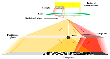
Figure 1. Scheme of an EH set-up in a TEM: part of the electron beam that has interacted with the sample (and possible surrounding stray fields) is overlapped to the part of the beam that has travelled through the vacuum thanks to an electrostatic biprism located resulting in the formation of an hologram in the detector plane.
Download figure:
Standard image High-resolution image
After these pioneering works, EH has been more and more developed these last 20 years in material science for the local investigations of electromagnetic fields and quantitatively map the magnetic and electrostatic fields appearing within and around a TEM thin specimen and to extract the associated physical properties at nanometer scale resolution.
As examples, EH provides an exceptional opportunity to locally study depletion region in p-n junction [8] or the activity of the dopant atoms in semiconductors studying the electrostatic potential modified by these dopants [9]. Through the quantitative analysis of the electrostatic field radiating around electrically charged nanostructures, Bellegia et al [10] and Gatel et al [11] have shown that the number of charges can been precisely measured to within a few charges. The magnetic configurations of various ferromagnetic (nano)materials, devices and even bacteria as a function of size and shape have been investigated with few angstrom resolution by EH [12–15] and, in some cases, even the 3D magnetic configuration has been revealed combining EH with tomography methods [16, 17]. In 2008, Hÿtch et al demonstrated that EH can also measure the phase shift of the electrons beams that are diffracted by a crystal [18] and therefore allows the measurement of the so-called 'geometric phase'. This 'dark-field electron holography' method permits mapping quantitatively the strain in stressed crystalline devices, and is now used by the semiconductor industries to determine the stress in strained metal-oxide-semiconductor transistors. The extent of this method for measuring the deformations in ferroelectric thin films is presented in this dedicated issue [19].
In very recent years, few groups have developed in situ EH experiments to analyze nanomaterial under various stimuli (i.e. temperature, (local) strain, magnetic fields) and/or to study devices in operando. Among the many different in situ EH experiments, let us highlight the local analysis of magnetic hysteresis loops in nanostructures [20, 21] the study of the magnetic field generating in a front of the pole of a hard disk writer in operando [22] and the in situ EH study of the electron emission from a polarized tip [10, 23].
In parallel to the development of EH for its application within the area of materials science, the technique itself has been growing for improved phase shift measurements [24] and new optical configuration with a multi-biprism set-up allows for more versatile experiments [25, 26]. These new optical developments for EH are reviewed in this issue by Tanigaki et al [27].
The scope of this issue aims to demonstrate these unique capabilities of EH to tackle scientific questions in materials science and more specifically those regarding high-resolution imaging, microelectronic, ferromagnetism, spintronics and field emission.