

Abstract
We fabricated flexible and transparent hydrogen gas sensors based on a palladium-decorated graphene mesh. Electron microscopy analysis confirmed that ~2–3 nm diameter Pd nanoparticles were uniformly dispersed on the graphene mesh surfaces. The sensors were highly transparent with an average optical transmission of >90% to visible light and they exhibited good electrical stability with a resistance change of 1.5% under a tensile strain of 1.1% in a cyclic bending-unbending test. Compared with graphene-based sensors, the graphene mesh sensors exhibited a faster response to hydrogen gas with sensitivity as high as ~5% at a low concentration of 10 ppm H2/air, even at room temperature. The enhanced H2 detection characteristic of the graphene mesh sensors is attributed to the existence of edges.
Export citation and abstract BibTeX RIS
1. Introduction
Concerns about environmental pollution and energy exhaustion have raised interest in clean and renewable hydrogen energy [1–4]. Following recent advancements in hydrogen handling techniques including storage, separation, purification, and transportation, hydrogen energy is now considered a promising alternative to fossil fuels [5–7]. One example of hydrogen use is fuel cell electrical vehicles, in which the primary electricity source is powered by hydrogen [1, 4, 8]. However, hydrogen has a low flammability point, and it is mainly stored and used at high pressure [9]. Therefore, to ensure safe hydrogen use a reliable hydrogen monitoring system is needed [9–12].
Palladium (Pd) has long been studied as a promising hydrogen sensing element since the absorption of hydrogen gas (molecules) by Pd was first found by Graham in 1866 [13]. However, despite its high reactivity and resistance change upon exposure to hydrogen at room temperature [10, 14–16], the structural degradation of rigid Pd film associated with volume expansion during the reaction with hydrogen (i.e. the formation of Pd hydride) [10, 16–18] restricts its long-term stability at hydrogen concentrations higher than 2%. At lower hydrogen concentrations the response time increases, especially at hydrogen concentrations lower than 1%, due to the low diffusion velocity of hydrogen in the Pd film [19].
To compensate for these drawbacks, Pd nanoparticles and carbon nanotube (CNT) hybrid structures have been proposed, where the resistance of the CNT channel is modulated by charge carrier transport through the Pd (or Pd hydride) and CNT contacts [12, 16, 20, 21]. This approach gave rise to a significant improvement in the performance of sensors, including higher sensitivity, long-term stability, and faster response. However, the coexistence of semiconducting and metallic nanotubes as well as the residuals and impurities remaining in the CNTs during the synthesis would degrade the device reliability [22]. In addition, the fabrication of the CNT-based devices generally requires the monodisperse assembly of the CNTs on the device substrates, which is hard to control and not well established [23]. More recently, graphene has been proposed as a substitute for CNT channels because its two-dimensional (2D) structure can facilitate large-scale patterning and the integration of devices with conventional fabrication techniques. In addition, graphene has several advantages inherent from CNTs. For example, as a one-atom-thick 2D material, all carbon atoms are exposed to the surrounding environment, thereby creating a low channel cross-section area [14, 24–28]. In addition, graphene has excellent charge transport characteristics and a low level of 1/f noise [25]. Finally, its mechanical flexibility and optical transparency can provide additional advantages for use in emerging areas. In particular, mechanically flexible sensors are suitable for use in the vicinity of intricate and irregular surfaces of hydrogen managing systems, such as hydrogen pipelines and connectors between a gas container and fuel cell. Despite the advantages of Pd-graphene hybrids, however, the transfer of charge carriers from Pd or Pd hydride to the chemically inert graphene surface has been significantly limited due to the relatively high contact barrier [26, 29]. In this study, graphene meshes with a circular hole array were prepared by direct chemical vapor deposition (CVD) and decorated with Pd nanoparticles for efficient hydrogen sensing. The edges of the graphene mesh are more energetically reactive than a pristine graphene lattice due to the dangling σ bonds, in which a chemical reaction with hydrogen can effectively lower the transport barrier for charge carriers. Due to these characteristics, a sensor based on a Pd nanoparticles-graphene mesh (Pd-GM) has enhanced sensitivity compared to a normal Pd-graphene (Pd-G) sensor with a comparable or slightly faster response to hydrogen gas. Moreover, our Pd-GM sensors were highly transparent in the visible range and reliable even under repeated mechanical deformation.
2. Experimental
2.1. Preparation of graphene and graphene mesh samples
Graphene and graphene mesh were prepared by CVD following previously developed procedures [30]. Both were grown on 25 μm-thick copper foils (99.999%, Alfa Aesar), although a hexagonally closed packed silica bead array was pre-deposited on a copper foil as a growth mask for the graphene mesh. In brief, the copper foils were placed inside a quartz tubular reactor and annealed at 1000 °C and 500–800 mTorr with a hydrogen gas flow for 30 min. Graphene growth was initiated by introducing methane gas. After 10 min of growth, the reactor was evacuated and cooled down to room temperature. The silica beads were removed by immersing the graphene sample in dilute 10% hydrofluoric acid for 5 min. After spin coating a polymethyl methacrylate (PMMA) protecting layer on the graphene and graphene mesh surface, the samples were placed in 0.05M ammonium persulfate solution to etch the underlying copper foils. The floating PMMA/graphene samples were then transferred to a flexible polyethylene terephthalate (PET) substrate. The PMMA film on the graphene and graphene mesh was removed by immersion in an acetone solution.
2.2. Hydrogen gas sensing measurement
Thin Pd layers were thermally evaporated onto the graphene and graphene mesh on PET substrates. During the evaporation, the deposition rates were controlled in the range of 0.1–0.2 Å s−1, and the evaporation was terminated when the total Pd thickness was measured to be 1–2 nm by a thickness monitor. The enamel coating at the ends of the copper wires was removed with sandpaper, and the wires were connected to the ends of Pd-G and Pd-GM sheets with silver paste and fixed with aluminum foil. The distances between the electrodes and the width of the graphene sheets are 10 mm and 5 mm, respectively. The device was annealed in air at 150 °C for more than 30 min. After annealing, the sensors were placed in a cylindrical stainless steel chamber (25 mm inner diameter) connected to electrical feedthrough and inlet/outlet lines for a gas mixture of dry hydrogen and dry air. The sensor responses were monitored under repeated flows of 100% air and mixtures of air and hydrogen gas, with a total flow rate of 100 sccm. For the measurements of the resistance changes with respect to either bending or hydrogen concentrations, a home-built I–V measurement system, consisting of a picoammeter (Keithley 6485) and data acquisition hardware (PCI 6221 card and BNC-2090a) were used.
3. Results and discussion
Graphene mesh decorated with Pd particles was transferred to a thermally oxidized Si substrate for scanning electron microscopy (SEM) investigation. As shown in figure 1(a), the Pd-GM had a hexagonal array of circular holes with an average diameter of ~350 nm, which is quite similar to bare graphene mesh, and there was no substantial difference before and after Pd deposition. To further investigate the morphology of Pd nanoparticles formed on graphene mesh, sample fragments were imaged with transmission electron microscopy (TEM). The TEM images showed that the deposited Pd formed individual, isolated nanoparticles rather than a continuous thin film. In addition, the Pd nanoparticles were homogeneously dispersed on the graphene mesh surface, and they had a uniform size distribution with an average diameter of ~2.85 nm (figures 1(b) and (c)). The formation of nanoparticles (i.e. island growth) rather than a 2D layer indicates that the inter-atomic attraction between the Pd atoms was stronger than the adhesive force between the Pd atoms and carbon atoms in the graphene lattice with low surface energy [14, 31]. The diffuse ring with a radius of 4.54 nm−1 in the fast Fourier transform (FFT) image (figure 1(c) inset) matched well with the (1 1 1) lattice-spacing of a face-centered-cubic (FCC) Pd crystal, indicating that Pd nanoparticles were mainly comprised of poly-crystalline Pd clusters [32, 33]. Raman spectroscopy confirmed that the graphene mesh mainly consisted of monolayer graphene with a low defect level (I2D/IG = ~1.88, ID/IG = ~0.20) (figure 1(d), black line). The slightly increased D peak intensity of the graphene mesh could be attributed to the edge defects. Even after Pd deposition, the graphene mesh maintained its structural characteristics as confirmed by the similar ID to IG ratio before and after Pd deposition (figure 1(d), red line).
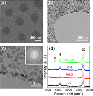
Figure 1. (a) SEM image and (b) TEM image of graphene mesh decorated with Pd nanoparticles. To prepare the TEM sample, fragments of the samples were picked up by a carbon legacy grid. (c) High-magnification TEM images highlighting the edge along the hole. FFT image of (c) is shown in the inset. (d) Comparison of Raman spectra of graphene (G) and graphene mesh (GM) sheets before and after Pd deposition.
Download figure:
Standard image High-resolution imageFigures 2(a) and (b) show a schematic illustration and photograph of the Pd-GM sensors fixed with two aluminum foil electrodes. Even after Pd deposition, the nanoparticulate film had fairly good optical transmission because light penetrated the gaps between the Pd islands [34, 35]. The Pd-GM on the PET substrate is almost invisible to the human eye with an optical transparency larger than 90% in the visible range (figure 2(c)).
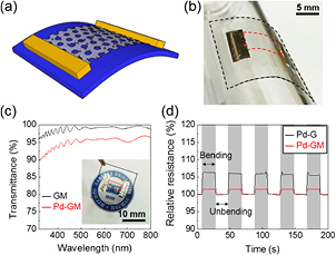
Figure 2. (a) Schematic of the sensor based on graphene mesh decorated with Pd nanoparticles (Pd-GM). (b) Photograph of the Pd-GM sensor laminated on the glass tube with a radius of ~0.84 cm. (c) Optical transmittance spectra of bare graphene mesh (GM, black) and Pd-decorated graphene mesh (Pd-GM, red). Inset: photograph of a fully fabricated Pd-GM sensor on PET substrate. (d) The relative resistance changes of the devices in the bending-unbending cycle test.
Download figure:
Standard image High-resolution imageTo evaluate the electrical and mechanical stability of the sensors, the current was measured at an applied voltage of 0.1 V during multiple bending-unbending cycles. The resulting resistance changes are plotted in figure 2(d). The sensor resistance increased by ~7.5% when bent with a tensile strain of 1.1% applied to the Pd-GM, but it fully recovered to the initial level when the sample returned to the unbent state (i.e. the strain was fully released). The resistance change in the bending state is associated with the distortion of the crystal structure of graphene. The broken hexagonal symmetry modifies the electronic band structure, and split the degeneracy of the energy bands, resulting in the resistance increase [36]. In addition, the distortion of the crystal lattice may cause additional scattering of charge carriers and increase the resistance [37]. Abrupt resistance changes were repeated at a constant magnitude for many cycles, demonstrating the mechanical flexibility and stability of the Pd-GM sheet. The relative change in the Pd-GM resistance was less than 1/4 that of the Pd-G (7.5% versus 1.5%). This result is attributed to the role of holes in graphene mesh, which deform in the bent state and compensate for some of the mechanical strain on the graphene lattice.
To test the sensing characteristics, the devices were placed in a stainless steel chamber connected to gas delivery lines. Continuous changes in resistance at different H2 gas concentrations were monitored at room temperature. Figures 3(a) and (b) show the relative resistance changes upon exposure to H2 gas at concentrations from 2 to 15 ppm. The gas sensitivity was defined as (R − R0)/R0, where R and R0 are the sensor resistance after and before exposure to H2 gas, respectively. Both the Pd-G and Pd-GM sensors had a noticeable change at concentrations as low as 2 ppm. To our knowledge, the sensitivity of our devices was greater than that of previous sensors based on Pd-CNT and Pd-graphene hybrid structures [10, 14, 21, 24]. The sensitivity was further improved by replacing graphene with graphene mesh at all measured H2 concentrations (figure 4(a)).
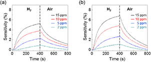
Figure 3. Variations of sensitivities of the sensors based on (a) Pd-G and (b) Pd-GM at different H2 gas concentrations. During the measurement, various concentrations of the target gas were introduced to reactor for 400 s, then the reactor was purged with air for 400 s.
Download figure:
Standard image High-resolution image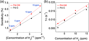
Figure 4. (a) Sensitivities as a function of the square root of H2 concentration. (b) The reciprocal response time (1/τ) with respect to H2 concentration.
Download figure:
Standard image High-resolution image
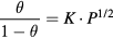
The sensitivities of both the Pd-G and Pd-GM sensors were linearly proportional to the square root of the H2 concentration, which agrees with predictions based on Langmuir adsorption isotherm theory [14, 16]. Assuming an equilibrium of the palladium hydride reaction  , the relationship between the surface fraction of the Pd particles occupied by the absorbed hydrogen (
 ) and the partial pressure of hydrogen (P) can be expressed as:
where the equilibrium constant,  , is defined as the ratio of adsorption to desorption rates. When the device was exposed to target hydrogen gas molecules, the hydrogen gas molecules divided into two single hydrogen atoms on the surface of the Pd nanoparticles by catalytic dissociation. Some dissociated hydrogen atoms reacted with the Pd nanoparticles and formed palladium hydrides. At this stage, the graphene channels acquired negative charge carriers (i.e. electrons) from Pd hydride [10, 12, 20, 21]. Since both graphene and graphene mesh have a p-type characteristic [30, 38], the sensor resistances increased in response to the electron injection from the Pd hydride particles. The other hydrogen atoms also diffused from the Pd nanoparticles to the graphene surface and formed adsorbates. In this case, the electrical properties of graphene might be rarely affected by the hydrogen adsorbates considering that pristine graphene is insensitive to the physical adsorption of hydrogen [39]. If hydrogen atoms diffused to defects such as the edges of the graphene mesh, however, they could have an effect. Carbon atoms at the edges of graphene mesh have a dangling bond and, thus, form chemical bonds easily with dissociated hydrogen atoms, thereby driving charge carrier transport to the graphene channel. Taking all things into consideration, the resistance (or conductance) of the gas sensor is mainly determined by hydrogen molecules absorbed on the Pd surface; dissociated hydrogen atoms can contribute to electron transfer to the graphene channel through either the hydride reaction or chemical bonding with carbon atoms at the defects. In both cases, the frequency is governed by
  ; thus, the resistance change (and sensitivity) is linearly proportional to
  if the H2 concentration is low enough that
  is much smaller than 1. This analysis also indicates that the enhanced sensitivity of the Pd-GM sensors is associated with the existence of edges.
Another important sensor parameter, the response time (τ), is defined as the time required for the sensor output (i.e., resistance change) to reach e−1 (~36.8%) of the maximum value upon exposure to the target gas, respectively [16]. The maximum output of the sensor indicates equilibrium between molecular adsorption and desorption at the Pd nanoparticle surface; thus, the response time is also affected by the partial pressure of hydrogen. Since hydrogen molecules can dissociate only at the surface of Pd nanoparticles, the supply of hydrogen atoms is restricted by hydrogen atom adsorption. Therefore, a considerable response was achieved at the initial stage and is main reason that the response time was decided by the partial pressure of hydrogen gas. The reciprocal response time (1/τ) had a linear correlation with the H2 concentration (figure 4(b)) [14, 16]. On the other hand, the recovery rate is mainly associated with the surface fraction of the Pd nanoparticles occupied by hydrogen molecules. As a result, the recovery rate is high at the initial stage, but it becomes gradually lower with time and finally goes to near zero [10]. This is the reason it takes a very long time to achieve a fully recovered state. Considering that graphene mesh has higher sensitivity, the number of transferred electrons should be higher for graphene mesh than graphene. Nevertheless, graphene mesh had a comparable or slightly faster response to H2 gas than did pristine graphene.
As mentioned earlier, the edges along the holes in the graphene mesh resulted in enhanced sensitivity. Carbon atoms at the edges have a dangling bond and easily bond with other molecules [30, 38], which gives the graphene mesh naturally strong p-type characteristics. In addition, the lower energy barrier at the edges could allow for fast charge transport between graphene and other absorbed materials, which is largely restricted in pristine graphene lattices. Although a small proportion of Pd nanoparticles were placed around the edges, they supported a fast response to H2 gas exposure.
4. Conclusions
We fabricated mechanically flexible and optically transparent hydrogen gas sensors by using graphene and graphene mesh decorated with Pd nanoparticles. Both sensors had a fast response and were highly sensitive to hydrogen with a sensitivity higher than 3.5% for graphene and 5% for graphene mesh sensors even at low hydrogen concentrations below 10 ppm. In particular, the sensor based on graphene mesh had enhanced H2 detection. The sensitivity measured at hydrogen concentrations of 2–15 pm were ~1.25 times higher for the Pd-GM sensor than for the Pd-G sensor. The enhanced sensing performance was associated with the edges of the graphene mesh, which led to increased carrier injection into the graphene channel over the lowered energy barrier through Pd hydridation or bonding between the carbon and hydrogen atoms.
Acknowledgments
This work was supported by the Basic Science Research Program (2015R1A2A2A11001426) and International Research & Development Program (2013K1A3A1A32035393) through the National Research Foundation of Korea (NRF) funded by the Ministry of Science, ICT and Future Planning (MSIP) of Korea. SN acknowledges the support from the Air Force Office of Scientific Research/Asian Office of Aerospace Research Development (AFOSR/AOARD) Nano Bio Info Technology (NBIT) Phase III Program (AOARD-13-4125).
Notes
The authors declare they have no competing financial interests.