
Abstract
The synthesis of silicon and silicon-based quantum dots (diameter < 5 nm) is discussed. Specifically the synthesis of Si-based quantum dots (QDs) by atmospheric pressure plasmas is reviewed and the most recent developments are also reported. Atmospheric pressure plasmas are then compared with other synthesis methods that include low pressure plasmas, wet chemistry, electrochemical etching and laser-based methods. Finally, progress in the synthesis of alloyed silicon QDs is discussed where the nanoscale Si–Sn and Si–C systems are reported. The report also includes a theoretical analysis that highlights some fundamental differences offered by plasmas at atmospheric pressure and that may provide opportunities for novel materials with advantageous properties.
Export citation and abstract BibTeX RIS

Content from this work may be used under the terms of the Creative Commons Attribution 3.0 licence. Any further distribution of this work must maintain attribution to the author(s) and the title of the work, journal citation and DOI.
1. Introduction
Silicon at the nanoscale offers a range of interesting features that have motivated intense research for a wide range of applications; research efforts have included nanowires [1], nanoparticles (NPs) [2] and more recently silicene [3–5] (the silicon-based graphene-like structure) for photovoltaics [6–8], photonics [7, 9], optoelectronics [10, 11], biological/biomedical applications [9, 12] etc. Some of the motivating factors for studying nanoscale silicon originate from the fundamental attributes of silicon as the chemical element: it is abundant, non-toxic and has a limited environmental footprint. In addition, the industrial infrastructure built around the microelectronic industry is also a valuable benefit that will allow nano-silicon research to progress into technological developments with reduced obstacles. In fact, the supply of raw materials, disposal of manufacturing waste and many of the industrial manufacturing steps for a nano-silicon industry may be able to rely on existing processes and know-how.
As with most nanotechnologies, silicon-based nanostructures offer beneficial properties due to an increased surface-to-volume ratio and the exploitation of this principle is, for example, the rationale behind silicon nanoparticles research for energy storage [13]. Similarly, the high aspect ratio of silicon nanowires can be advantageous in improving the collection efficiency in solar cells by offering large junction interface area with short and effective collection paths for photo-generated carriers [6]. In order to exploit these advantages, silicon nanostructures can have dimensions typically above 10 nm and most optimal application results have been often achieved for nanoparticles/nanowires with diameters in the range 20–100 nm [14, 15].
In addition to the surface-to-volume ratio, 3D spatial confinement also represents a very important nanotechnology feature. For silicon, new optoelectronic regimes can be observed when the NP is reduced well below 10 nm (weak quantum confinement [10]). However, interesting novel phenomena become truly apparent only within the strong quantum confinement regime [10], i.e. when the diameter is comparable or below the silicon Bohr radius (~4.2 nm); in these cases the silicon nanoparticles are referred to as quantum dots (QDs). Weak and strong quantum confinement both present useful but differing features and it is therefore important to underline that the resulting properties of weakly confined silicon NPs and strongly confined QDs can be drastically different. For example, the electron–hole Coulomb interaction that enables the existence of excitons in the weakly confined regime is dominated by confinement effects in the strong confinement regime, leading to uncorrelated motion of electrons and holes.
The surface properties of silicon QDs have a strong influence on the effects of quantum confinement, and due to very reactive nature of such surfaces, a wide range of experimental results have been reported for Si QDs that are nominally similar. For instance, varying the coordination and surface arrangement of oxygen-terminated Si QDs can impact dramatically on the optical [16] and transport [17] properties due to the overlapping core/surface wavefunctions as well as the short distances that electrons, holes and excitons can travel, therefore affecting both the energy structure and the transition dynamics [16]. This is further complicated by the indirect nature of silicon band structure where direct and indirect transitions may arise in competition. Although these aspects have delayed the understanding and application of Si QDs, in comparison to, say, Pb-based QDs (e.g. [18–20]), they also offer an incredible opportunity to develop QDs with a higher degree of functionality. Additional opportunities for Si QDs also come from pairing silicon with other group IV elements such as carbon and tin (which are also abundant, non-toxic and environmentally friendly as silicon). Alloying silicon with carbon and tin, so called composition tuning, allows for an added degree of control over the QD band energy structure allowing manipulation of the bandgap as well as adjustment of the direct/indirect nature of the semiconductor [21].
The interplay of quantum confinement, surface effects, direct/indirect behaviour and composition tuning can lead to a wealth of prospects available only through Si-based QDs. However realisation of such prospects requires much greater control and versatility in QD synthesis in order to sustain, initially, the fundamental research and then offer methodologies for prototyping and eventually industrial implementation. Therefore, in order to study and exploit the benefits of quantum confinement, particularly in the strong confinement regime, it is important that synthesis methods reliably and accurately produce silicon QDs with a selectable size and a narrowly size distribution and facilitate diverse and accurate surface engineering.
In this contribution we will report on the synthesis and surface engineering methods for Si-based QDs (i.e. within the strong quantum confinement regime), made out of elemental silicon and the binary systems silicon–carbon and silicon–tin. We will limit our attention to 'free-standing' Si-based QDs (i.e. not embedded within a bulk matrix and not grown epitaxially on a substrate); this is because Si QDs that are not free-standing present substantial fundamental differences (e.g. matrix-induced mechanical strain), different synthesis challenges and different application focus (e.g. not suitable for applications that require colloids). Specifically, the focus will be on non-equilibrium low-temperature plasma processes at atmospheric pressure which represent the 'youngest' technique for the synthesis of Si-based nanostructures and may offer features not available with other methods. These processes include gas-phase plasma discharges, plasma discharges in contact with liquids and laser-produced plasmas within liquids all at atmospheric pressure. Because laser-produced plasmas in liquid belong to a well-developed field [22], only the more recent developments on alloyed QDs will be reported here and the reader is referred to the relevant literature on the synthesis of elemental silicon QDs with laser-produced plasmas in liquids (e.g. [22]).
Firstly, a brief overview of other synthesis techniques will highlight their advantages and disadvantages, and the need for further research into synthesis capabilities. The synthesis of Si QDs by atmospheric pressure plasmas will be then reviewed and compared with the other synthesis techniques on the basis of defined figures of merit. A simplified theoretical analysis on the characteristics of the plasma regime at atmospheric pressure regime will be also given. Finally, the most recent advances using atmospheric pressure plasmas will be described where the synthesis of high quality elemental Si QDs, SiSn QDs, SiC QDs are demonstrated and the tuning of optical properties is achieved through surface engineering. An outlook on future directions that include amorphous Si QDs concludes this report.
2. Synthesis of silicon quantum dots
2.1. Atmospheric pressure plasmas for the synthesis of silicon quantum dots: a brief review
Atmospheric pressure plasmas come in a wide range of reactor sizes [23]; nonetheless for the synthesis of nanomaterials, microplasma reactors have represented the workhorse [24–26]. This is because microplasmas offer the simplicity, low-cost and versatility required for explorative research; while challenges do exist in scaling up microplasma reactors, plasma research is already producing a range of industrially viable solutions ([27–30], see also further below).
Synthesis of Si QDs in atmospheric pressure plasmas has been reported by several groups only within the last decade. The first attempt was reported by Sankaran et al [31] where a direct-current (DC) microplasma was employed for the synthesis of Si QDs; this configuration was highly successful for the synthesis of a wide range of other NPs including crystalline elemental and bi-metallic NPs [24, 32]. The discharge is based on a micro-hollow cathode configuration generated between a metal capillary as cathode and a second metal tubing as anode. The background gas and silane precursor is introduced into the metal capillary. The discharge is powered with a dc power supply and high values of the delivered power density have been measured for the plasma (~5000 W cm−3 [31]). Thus a highly reactive plasma is expected in accordance with the properties of micro-hollow cathode discharges. The residence time of the growing particles inside the plasma is very short (<1 ms) allowing formation of QDs in the strong quantum confinement regime, with small diameters (<5 nm [31]). The blue luminescence at room temperature with quantum efficiency of 30% was reported for their Si QDs. The synthesis rates reported in this case is one of the main drawbacks, with collection times as long as 24 h to achieve sufficient quantities suitable for characterization [31]. This could be due to a combination of factors that include the dc-driven configuration in combination with the precursor chemistry [31]. While this work remains an important milestone for Si QDs synthesis, this approach has major limitation in terms of QDs production throughput and scaling-up to deposition in large surface areas.
More recently, with the aim of better understanding the mechanisms and chemistry involved in the micro-hollow cathode dc-microplasma, Barwe et al [33] developed a dc microplasma reactor analogous to the one reported by Sanakaran et al [31]; however plasma diagnostic tools were employed providing important and useful details. Barwe et al [33] also investigated the effect of hydrogen (0–5000 ppm) with silane (1.25–2.5 ppm) as precursor in an argon background (100 sccm). In their study, the results from emission spectroscopy of the plasma confirmed efficient dissociation of the silane and the consistent presence of atomic Si in the plasma. The dissociation efficiency however seems to be affected by the silane concentration where for concentrations higher than 20 ppm an increase in power would be required to produce silicon atomization. A fast camera imaging also showed that the plasma was not located inside the hollow cathode, but it appeared as a moving filamentary microplasma between cathode and anode. As a result, only a part of the gas flow (including precursor) that passes through the cathode tubing was interacting with the plasma. This may explain the low QDs synthesis yield and low throughput in this reactor. The results from transmission electron microscopy (TEM) of the samples prepared with different ratios of silane/hydrogen showed the growth of crystalline Si QDs only at higher hydrogen content; crystalline QDs were observed for 1.25 ppm silane and 260 ppm hydrogen. The TEM images show that the QDs are embedded in larger oxidized amorphous materials and the average diameter of 4 nm was determined by dynamic light scattering (DLS). The study therefore revealed fundamental information; however it also confirmed the limits of the dc-excitation and its configuration.
Efforts to improve the synthesis rates were produced by Nozaki et al [34], where both the precursor chemistry and configuration were changed with respect to prior work. Nozaki et al reported the synthesis of Si QDs using silicon tetrachloride as precursor and a radio-frequency (RF; 144 MHz) atmospheric pressure microplasma sustained by two ring-electrodes (similar to figure 1(a)); essentially this configuration represented a miniature atmospheric-pressure version of the plasma configuration that was extensively used for the synthesis of silicon QDs at low-pressure (see figure 6 [35]). The introduction of hydrogen in the synthesis chemistry was also investigated by Nozaki et al [34] and its effect on the deposition rate, crystalline/amorphous structure and photoluminescence of QDs was explored. It was observed that H2 enhances the deposition rate several times and also increases the crystallization degree; e.g. the samples produced without H2 contained amorphous NPs while crystalline QDs are observed when 0.7% H2 was used. Similarly, the synthesis rate was largely increased by almost ten times introducing up to 3% H2.
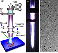
Figure 1. The 'two-ring' configuration used for the synthesis of silicon quantum dots (QDs). (a) Schematic diagram of the microplasma reactor; (b) photo of the microplasma generated inside the quartz capillary; (c) representative transmission electron microscopy image of the silicon QDs synthesized in the microplasma. Reprinted with permission from [39], Copyright 2014 AIP Publishing.
Download figure:
Standard image High-resolution imageIn the past few years, we have studied the synthesis of Si QDs in several atmospheric pressure microplasma reactors [36]. The study established both the effectiveness of RF-driven as well as the versatility of atmospheric pressure microplasmas in investigating synthesis conditions and exploring nanoscale materials. Significant improvements both in terms of quality and production rates have been achieved with a modified scalable microreactor configuration (see further below [37, 38]). At the same time, the 'two-ring' configuration (figures 1(a) and (b)) was confirmed to be effective in the synthesis of Si QDs (~2 nm in diameter, figure 1(c)) at higher production rates with silane precursor (10 ppm in argon) and the role of hydrogen was also clarified [39]. This microplasma also showed electron densities as high as 1.8 × 1014 cm−3 with gas temperature as low as 490 K determined by optical emission spectroscopy [39].
Typical results from TEM analysis of the Si QDs are shown in figure 1(c), which shows that the collected QDs are very well separated without any agglomeration. Further analysis of the QDs using high resolution TEM and dark-field images [39] shows that the QDs are crystalline and narrowly distributed. These results therefore showed significant progress in synthesizing high quality Si QDs in the strong confinement regime in this type of plasmas; in particular it was shown that control of size, reduced aggregation and absence of amorphous material could be achieved.
From the work carried out so far some conclusions can be drawn. Atmospheric pressure microplasmas provide a valuable tool to study synthesis mechanisms at atmospheric pressure where the configuration of the reactor can strongly affect the synthesis mechanisms and capabilities. A configuration that allows for a continuous flow-through process is highly desirable to offer advantages over other methods. RF excitation frequencies appear to be well suited for Si QDs synthesis and certainly more effective in providing higher synthesis rates compared with dc excitation. At this time, 13.56 and 144 MHz are the only frequencies that have been investigated and there is no doubt that this parameter can strongly affect and possibly improve the capabilities of atmospheric pressure plasmas (e.g. kHz or >144 MHz should be explored). Atmospheric pressure plasmas have shown to have the flexibility to deal with differing chemistries (SiH4 and SiCl4) and with/without the contribution of hydrogen. In particular, hydrogen seems to have a different role if compared to its effect in low-pressure plasmas [40–42]. While in low-pressure plasmas SiHx radicals seem to largely contribute to the nucleation of Si QDs [40], in atmospheric pressure plasmas silicon atomization [36, 37, 43] appears to be a common essential feature in the synthesis of Si QDs at atmospheric pressure. With regard to precursors, it is difficult to establish whether SiH4 or SiCl4 is preferable, as the selection has been so far determined by health and safety regulations and possibly by the researchers' familiarity with one or the other precursor/precursor chemistry. It is important to mention that possible avenues exist for other silicon precursors (e.g. SiBr4 [44]) including liquid or even solids. It is also worth noting that all reports have used argon as background gas for Si QDs synthesis whereas helium is generally the preferred choice for many atmospheric pressure plasmas applications. While this has ultimately a positive impact in the cost of future manufacturing processes, the reason behind the use of argon might have more fundamental justifications. Helium is a very good 'cooling' background gas and, as will be discussed later, the possibility of tuning the gas temperature is key to the successful crystallization of the Si QDs. Atmospheric pressure plasma reactor designs should also be improved to overcome some practical and engineering challenges. For instance deposition within the walls of the micro-channel reactors may shorten the operation time, requiring maintenance or replacement of the reactor. Current micro-reactor designs (e.g. figure 1) can however be operated for several hours (>3 h) without observing any negative impact due to wall deposition; the micro-hollow cathode has been operated up to at least 24 h [31]. The simplicity of these reactors also allows easy and quick replacement of low-cost contaminated components, which hardly hinders research activities. It is clear that several other solutions are possible if an industrial application was to be implemented; for instance preliminary results (not reported yet) have shown that shroud inert gas flow can potentially eliminate wall deposition and allow for non-stop operation. Another approach to ensure consistent quality of the synthesized QDs is to implement matching compensation so that the plasma conditions are kept constant over time.
Compared to low-pressure plasmas, atmospheric pressure plasmas have been subject of only a very limited number of studies and hence a much greater research effort is required with extensive room for improvements; the study of the synthesis mechanisms in atmospheric pressure plasmas is probably 10–20 years behind that of low-pressure processes and much more if the initial studies on undesired particles formation in low pressure silane plasmas is also considered.
2.2. Recent progress with atmospheric pressure plasma for silicon quantum dot synthesis
The reactors geometries developed so far have allowed initial progress for the synthesis of Si QDs by atmospheric pressure plasmas; nonetheless both the micro-hollow cathode and the two-ring configurations cannot be easily scaled up and engineering these reactors in arrays introduces non-trivial challenges. We have therefore developed a new reactor design that could offer opportunities to increase both the absolute throughput as well as the deposition area of Si QDs (figure 2) [36–38].
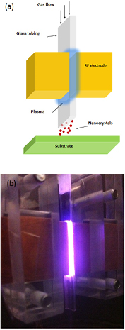
Figure 2. (a) Schematic of the 'cross-flow' atmospheric-pressure plasma reactor; RF stands for radio-frequency. (b) Photo of helium (1000 sccm) plasma sustained with the cross-flow reactor at 100 W applied power.
Download figure:
Standard image High-resolution imageThe geometry of this reactor is characterized by the electric field developed across the electrodes, which is normal to the direction of the flow; both the two-ring and the micro-hollow cathode configurations had the applied potential along the flow direction. We will refer to the geometry of figure 2 as the 'cross-flow' configuration. A key element of the system is a rectangular quartz tube with an internal cross section of 0.5 × 5 mm and 0.3 mm wall thickness. The plasma is created within the 0.5 mm gap by applying RF-power (13.56 MHz) through two rectangular copper electrodes (figures 2(a) and (b)). The dimensions of the electrodes are designed to match with the quartz tube width (5 mm) and are 20 mm long. A frame made out of Perspex holds all the components together.
This cross-flow configuration has demonstrated the synthesis of Si QDs with superior quality. An example of the Si QDs synthesized is presented in figure 3(a), which displays a TEM micrograph where Si QDs with a narrow size distribution centered at ~2.5 nm are observed. Diffraction and composition analysis have provided clear evidence of the crystallinity of these Si QDs [38].
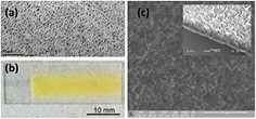
Figure 3. (a) Transmission electron microscope image of Si quantum dots (QDs) prepared using the 'cross-flow' configuration. (b) Photograph of a thin film of Si QDs (yellowish area) deposited on a patterned indium–tin-oxide coated glass substrate. (c) Scanning electron microscopy (SEM) image of a thin film of Si QDs prepared with the cross-flow deposition system. The inset shows a cross section SEM image to illustrate the thickness of the thin film grown.
Download figure:
Standard image High-resolution imageThe Si QDs reported in figure 3 were produced with 50 ppm silane and 0.3% hydrogen in argon background (1000 sccm total flow). The applied power was 100 W. Additionally we have equipped the reactor with an X–Y stage to enable the movement of the substrates during the deposition, allowing the deposition of homogeneous thin films of Si QDs (see figures 3(b) and (c)). Implementing Si QDs in a device entails in most of the cases the formation of a homogenous film with controlled thickness, so that our set-up is now routinely used for photovoltaic device fabrication. Scanning electron microscopy (SEM) images of these films are displayed in figure 3(c) and reveal that Si QDs are forming a porous film; the control of the film porosity and the formation of compact films will be an aspect for future investigations as it is important for a wide range of applications.
While high quality Si QDs can be achieved also with the two-ring reactor, the cross-flow design has two main advantages in terms of scalability and synthesis throughput. Because the plasma conditions are dictated by the electrode gap, in the cross-flow configuration it is possible, in principle, to extend indefinitely the length and width of the plasma without affecting the plasma properties and therefore preserving the synthesis conditions. This was not possible for instance with the two-ring configuration where a longer plasma necessarily required increasing the gap between the electrodes and consequently would necessitate higher voltages to be ignited and sustained; therefore, the plasma extension in the flow direction of the two-ring configuration is limited as, at some point, the required voltage would be too high or would restrict the plasma parameter space outside suitable synthesis conditions. Increasing the length of the plasma along the flow direction is important for increasing the overall synthesis throughput (i.e. a higher number of QDs can be produced per unit time) as a 'longer' plasma allows for increasing the total gas flow while keeping the same residence time; this will be discussed later in more details (section 2.3.2). Therefore, a promising feature of this reactor is a higher throughput than that achievable with the two-ring configuration and comparable to that of other vacuum plasma techniques. The two-ring and micro-hollow cathode configurations have also intrinsic limitations in extending the width or cross section of the plasma, which would allow a larger surface area to be covered (per unit time) when depositing for instance thin films of Si QDs as in figure 3. A larger surface area can be achieved with the two-ring or micro-hollow cathode configuration only by engineering microplasma arrays, with consequent design complications. Again the cross-flow approach allows easily the extension of the width with no impact on the synthesis conditions.
Although used only for carbon-based nanomaterials, the possibility of scaling up the cross-flow configuration was already demonstrated (figure 4 [27]). Figure 4 shows a larger implementation of the cross-flow design. In this case the plasma was formed with bare electrodes (i.e. no glass capillary was used) ~5 cm wide and 10 cm long and with a variable gap in the range 0.3–0.8 mm.
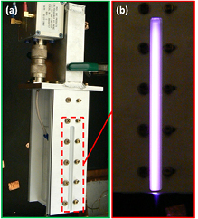
Figure 4. (a) Scaled-up atmospheric pressure plasma reactor in a cross-flow configuration. (b) Photo of the side view of the ignited plasma.
Download figure:
Standard image High-resolution imageTo conclude this section, we report here some results produced for the synthesis of amorphous Si QDs [36]; while most of the attention is generally devoted to the formation of crystalline QDs, amorphous QDs do have some fundamental scientific interest and may find application in a range of applications (e.g. [45–47]). Amorphous Si QDs were produced in the cross-flow configuration. However in this case a round glass capillary (0.7 mm internal diameter and 1 mm external diameter) was used in place of the rectangular capillary of figure 2(b) and the electrode were 1 cm long; figure 5(a) shows an argon plasma produced with this reactor.
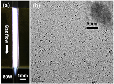
Figure 5. (a) Photographs of an argon, 250 standard cubic cm (sccm), plasma in the cross-flow configuration for an applied radio-frequency power of 80 W. (b) Amorphous silicon quantum dots produced with the cross-flow configuration in (a) but operated at 100 W with helium background gas and 200 part per million silane; the total gas flow was 800 sccm.
Download figure:
Standard image High-resolution imageFigure 5(b) shows a TEM image of the QDs synthesized (~6 nm diameter average) in this reactor using silane (200 ppm) as precursor and helium as buffer gas with the total gas flow rate of 800 sccm and an applied power of 100 W. QDs in figure 5(b) were collected directly in ethanol and then drop-casted on the TEM grid. We have been able to vary the average diameter in the range ~1–10 nm by changing the silane concentration (10–200 ppm) with a corresponding photoluminescence (PL) shift [36]. Quantum confinement in amorphous QDs has not been studied experimentally; however theoretical investigations support the observation of a blue shift of the PL peak wavelength with decreasing size of the NPs [48]. The results from high resolution TEM analysis of Si QDs in this reactor for different conditions show that the produced QDs are amorphous (e.g. inset of figure 5). Further chemical analysis of the QDs using XPS and FTIR showed that the QDs are Si QDs with a possible degree of hydrogenation possibly not limited to the surface ([36] and Supporting Information) (stacks.iop.org/JPhysD/48/314002/mmedia); however, the level of hydrogenation, will require further in-depth study which will be reported separately. XPS analysis reveals the dominance of metallic silicon peak which confirms the presence of Si–Si bonds in the core of the QDs while the minor oxidation peaks are attributed to the surface oxidation in accordance with the literature ([36] and references therein). This has been supported also with the data from FTIR (see Supporting Information) (stacks.iop.org/JPhysD/48/314002/mmedia): although the presence of partial oxidation cannot be denied, the low (or negligible) intensity of the characteristic oxide peaks at 1100 cm−1 evidences the low degree of surface oxidation of the samples, as these peaks are commonly stronger in the reported spectra in literature ([36] and references therein).
Nucleation and growth of amorphous Si NPs in this reactor can be understood through the study of the plasma parameters. As it will be discussed in more detail later, for the formation of amorphous QDs, the plasma conditions were such to maintain a low gas temperature (e.g. ~355 K measured by optical emission spectroscopy with 250 sccm argon and 100 W applied power [36]). This implied that even if the NPs were selectively heated above the gas temperature, their temperature never reached values close to the crystallization temperature. These amorphous QDs showed interesting size-dependent optical properties that are of great scientific interest [45–47]. Importantly, these results demonstrate that atmospheric pressure plasmas can synthesize, in a controlled manner, amorphous QDs as well as crystalline QDs.
2.3. A comparison of atmospheric pressure plasma synthesis with other synthesis methodologies
2.3.1. Methods for the synthesis of silicon quantum dots.
Over the last decades, several methods for the synthesis of Si QDs have been investigated, including a range of plasma-based, laser-based and wet chemistry methods. Some of these techniques such as thermal plasmas and laser pyrolysis have been highly successful in producing large quantities of Si NPs at low cost, which are useful for a number of applications [49–51], but they have not been able to produce NPs of sufficient quality for applications where the strong quantum confinement regime is required (i.e. QDs with <5 nm diameter). For this reason, we will focus our attention only on techniques that have demonstrated synthesis capabilities with size distributions fully within the strong confinement regime. As this section is not intended to be a review of all synthesis methods, only a few selected representative works will be used for the comparison with atmospheric pressure plasma synthesis.
Porous silicon (PS) by electrochemical etching.
Electrochemical etching of Si wafers in hydrofluoric acid (HF) was one of the first methods used intentionally to produce Si NPs (e.g. [43, 52–55]). Silicon wafers are etched by applying a current to an HF-based solution in contact with the wafer. The process produces a PS layer of nano-sized or micro-sized crystallites, depending on etching conditions, on top of the wafer that can then be removed in various ways (e.g. by sonication, applying a high current pulse or by mechanical pulverization). One of the main advantages of this method is that it can easily produce doped Si QDs, starting from either p-type or n-type wafers; the main disadvantage is that QDs are aggregated in the porous structure and complete fragmentation in single and separate nanocrystals is very difficult and laborious.
Low pressure plasmas (LPPs).
The formation of nano-sized crystals via LPPs based on silane gas chemistry has been known for many years, although this was initially an undesired effect in silicon processes used for the microelectronic industry. The formation of NPs in LPPs represented therefore a problem, which motivated extensive research to understand silane dissociation and subsequent NPs nucleation, although the aim of these studies was to prevent NPs growth. With the growing interest in nanoscale silicon, this knowledge and expertise was exploited to control NPs formation and therefore Si NPs synthesis by LPPs was initially carried out using standard RF parallel-plate configurations [56–58]. Cabarrocas et al [56] employed a pulsed capacitively-coupled plasma for the synthesis of Si NPs with size in the range ~6–12 nm. Control over size was achieved through changing the duration of the pulse. A sophisticated microwave-excited plasma reactor was also used for the synthesis of NPs with size in the range 6–11 nm where control over size was possible through adjusting silane concentration [57, 58]. These methodologies however highlighted some difficulties in reducing the size to less than 5 nm in diameter and the QDs could be produced mainly with post-synthesis HF-based solution etching [58]. A significant breakthrough was achieved by designing ad-hoc flow-through plasma reactors (e.g. [35]) that allowed improved control over the time that a growing NP would spend within the reactive plasma environment, i.e. the 'residence time'. This residence time determines the extent of NP growth and therefore an accurate control of short residence times is required for QD synthesis. Figure 6 shows an RF plasma reactor reported by Mangolini et al for the synthesis of group IV NPs [35]. The configuration consisted of a glass tube with two copper ring electrodes (i.e. in the 'two-ring' configuration). The NPs produced in the plasma were collected on a stainless steel mesh positioned in the exhaust stream (figure 6).
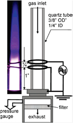
Figure 6. Low-pressure plasma reactor presented by Mangolini et al for the synthesis of quantum-confined nanoparticles [35]. Reprinted with permission from [35], Copyright 2014 ACS Publishing.
Download figure:
Standard image High-resolution imageIn addition to silicon, synthesis of other NPs including germanium was reported [40], with size and crystallinity control of small NPs (<10 nm) made possible through changing the residence time and also, with a weaker dependence, by changing the precursor concentration. Si QDs with diameters from 3 nm were reported by changing the residence time from 2 ms [35]. The particle size distribution was also rather narrow with a standard deviation of 10–15%. It was also found that applied RF power is the most effective parameter in determining the degree of crystallinity of the NPs, varying from amorphous to crystalline by varying the applied power from 25 to 85 W [59]. This LPP approach has now reached very high synthesis standards (e.g. [17, 40–42]) and has delivered the best results for photovoltaics thus far [17], which is one of the applications with the most demanding quality requirements for Si QDs.
Laser ablation (LAL) in liquids.
Švrček et al [60] and Intartaglia et al [61] among others [22] have demonstrated the synthesis of luminescent Si QDs via a laser ablation in liquids approach. Although Si QDs can be produced easily with this technique, the size distribution is relatively large and scaling up has also some limitations. Nevertheless, LAL represents a very powerful and versatile tool for exploring new materials and materials compositions; this will be evident later in this manuscript when alloyed Si QDs will be discussed [21].
Wet chemistry (WC).
Methods based on WC have been widely used for the synthesis of group II–VI and IV–VI compound semiconductor QDs. In the case of group IV materials such as silicon, obtaining the crystalline structure generally requires high temperatures although synthesis of Si QDs by WC has been reported in a number of works (e.g. [62–68]). For example Zhang et al [62] reported the synthesis of Si QDs with average diameter of 4 nm using solution routes. Their QDs were coated with polymers and had stable blue photoluminescence with 32% quantum yield in ethanol and 18% in water. Shirahata et al [63] reported synthesis of small (<2 nm diameter) Si QDs with emission between 300 to 450 nm by reduction of SiCl4 using a microemulsion method. Kauzlarich et al presented the synthesis of QDs with average diameter of 4.5 nm [64]. In general, a few different chemical routes with various chemistries involved have been reported. Very intensive heat processes at high temperatures are often required to achieve silicon crystallization (1000–1900 °C [67, 68]), however there are reports of apparent room temperatures synthesis of crystalline Si QDs [63–66]. In all cases the synthesis requires long reaction times (hours to days, e.g. 4–5 h [65], 15–16 h [63], 48 h [62] etc) and additional sequences of lengthy and complicated procedures are required (e.g. up to days [63]) for precursor preparation as well as for post-treatment, etching, waste removal etc. The possibility of producing crystalline structures with WC methods at room temperature is still puzzling and not fully explained from a physical point of view; however, it is apparent that the energy required to crystallize the QDs has to come in very small doses through surface exothermic reactions during the growth. This interpretation may be justified by the very long time required (4–48 h [62, 63, 65]) for the synthesis through these chemical routes.
2.3.2. Comparison with other synthesis methods and figures of merit.
In order to provide a framework for the comparison with atmospheric pressure plasmas, we have identified qualitative and quantitative figures of merit that can be used to assess the QDs quality and industrial potential feasibility of synthesis methods (see table 1). While some of these figures of merit are in principle quantitative, it has been often difficult to extract precise values from the literature due to the very early research stage of some of the works reported.
Table 1. Comparison table among different silicon quantum dots synthesis methods with respect to defined figures of merit.
| Atmospheric pressure plasmas—APP | 'Porous silicon'—PS | Low-pressure plasmas—LPP | Laser ablation in liquid—LA | Wet chemistry—WC | |
|---|---|---|---|---|---|
| QDs quality | |||||
| Control over crystalline fraction | Good | Medium | Good | Medium | Medium |
| Size control (average/distribution) | Good | Good | Good | Poor | Medium |
| Collection/Deposition | • Powder | • Powder | • Powder | • Colloids | • Colloids |
| • Films | • Films | ||||
| • Colloids | |||||
| Suitability for surface engineering | Good | Poor | Medium | Poor | Poor |
| Industrial feasibility | |||||
| Absolute throughput (kg h−1) | 10−7 | 10−9–10−6 | 10−5 | 10−9–10−6 | 10−6–10−5 |
| Throughput scalability | • Increasing flow | • Increasing N. reactors | • Increasing flow | • Increasing N. reactors | • Increasing N. reactors |
| • Increasing dimensions | • Increasing N. reactors | ||||
| • Increasing N. reactors | |||||
| Throughput density (kg h−1 m−2) | 1.2 × 10⁻¹³ | n.a. | 4.4 × 10⁻¹³–5.2 × 10⁻¹¹ | n.a. | n.a. |
| Cost ($ kg−1) | Low | Medium | Medium | Medium | High |
| References | This work, see above | [24, 69] | [44, 70] | [24, 71–74] | [67, 68] |
Crystallinity fraction (% weight).
Many of the techniques described above produce QDs together with undesired amorphous material. Therefore the amount of viable crystalline QDs versus uncontrolled amorphous silicon growth represents an important parameter in defining the quality of the synthesis methods. The crystalline structure of QDs is important for many applications as amorphous QDs have more defects and trap states which can deteriorate the optoelectronic properties of the material. However for some applications, the amorphous nature of the QDs might be preferred [45–47] and therefore control over crystalline versus amorphous content is the important parameter rather than simply the ability of producing solely crystalline QDs; the synthesis method should be able to 'switch' easily from ~0% to ~100% crystalline fraction. Although quantification of the crystalline fraction can be in principle determined through Raman spectroscopy [42], the sophisticated theoretical models that describe the interaction of the Raman laser light with the Si QDs are not available [42]. It follows therefore that only semi-quantitative values or indicative labels can be determined and hence in table 1, crystallinity control is labelled qualitatively as 'good', 'medium' or 'poor'. Similar qualitative descriptions are given also for other parameters where quantification was difficult.
Because PS is produced from single crystal silicon wafers, the fraction of crystalline material is relatively high and for this reason, electrochemical etching is unable to produce fully amorphous Si QDs. LPPs on the other hand can easily yield very high crystalline fraction and by modulating the power, fully amorphous QDs can be also produced. LAL, due to the very high power density, necessarily triggers interactions of the ablated silicon atoms within the liquid environment leading to the formation of amorphous material (e.g. oxide) [61]. In principle, by varying the laser pulse energy, repetition rate etc it should be possible to reduce or enhance the amorphous fraction. WC methods have exhibited relatively high crystallinity fraction although a range of post-synthesis processes are applied to yield crystalline Si QDs [67, 68] and currently there are no studies available that show the ability of synthesizing amorphous Si QDs. Atmospheric pressure plasmas (APPs), as in the case of LPPs, are now capable of very accurate control over crystallinity and have demonstrated 'switching' from crystalline to amorphous QDs. The reason for this superior control by plasma processes (both APPs and LPPs) is due to the non-equilibrium environment that allows for separate mechanisms, one that determine the nucleation/growth of NPs and the other that determine the NPs heating and therefore the supply of the required energy for crystallization.
Size control.
The crystallinity/amorphous nature of Si QDs is not the only important property to be considered in a synthesis approach. Other properties such as mono-dispersity and control over average size are crucial for some applications, more so if properties originating from the strong confinement regime are sought after. The size of QDs can be characterized by an average diameter together with a value representing the dispersion of the distribution which generally follows either a normal or a log-normal distribution. The most reliable characterization method to determine size parameters is to conduct a statistical analysis from TEM images, supported by either x-ray diffraction (XRD) analysis through the Scherrer equation or Raman spectroscopy coupled to theoretical models [42]. Unfortunately, other methods (e.g. DLS) have often resulted in misleading results when they were not 'calibrated' with one of the methods above (i.e. TEM & XRD/Raman). The size and size distribution is generally more important for applications that rely on optoelectronic properties of the Si QDs (e.g. photovoltaics, light-emitting devices etc); biological and medical applications, although they can make use of size-dependent optical properties, they generally have less demanding requirements in terms of size distribution. Energy storage, for instance, is an application where a relatively large size distribution is not very detrimental to the device performance.
For PS, the analysis of the QDs size (using TEM statistical analysis) is very challenging due to the aggregated state of the QDs [43]; observing the crystalline nature is possible for only a few QDs for each focal plane making statistical analysis expensive and tedious. Nevertheless, limited TEM analysis combined with XRD results have shown that electrochemical etching is capable of controlling the size of the QDs (<5 nm diameter) with narrow distributions [75–78]; this is confirmed by the tunability of PS photoluminescence [75–78]. Synthesis by LPPs shows superior control over the size and size distribution compared to the other methods with control of the residence time being a key factor leading to Si QDs with arguably the best size distributions. LAL offers improvements in size control with respect to laser pyrolysis or laser ablation of solid targets in gas-phase as the laser-produced plasma plume can be confined within the liquid environment. However, it is generally worse than plasma-based methods. WC methods appear to have a reasonable control over the size although the post-synthesis steps are again extensive and may contribute to narrow the size distribution and eliminate out of range NPs. With the most recent progress, APPs have demonstrated the capability of producing high quality size-controlled QDs comparable to those produced by LPPs.
Collection/Deposition.
An important aspect of synthesis methods is the collection of QDs/NPs, which needs to be suitable for the targeted application. In most cases, QDs are needed either in colloids or deposited on substrates or integrated directly into application devices.
WC and LAL necessarily produce QDs colloids; the deposition on substrates therefore requires additional steps which can sometime introduce additional difficulties or waste of QDs (e.g. spin coating). Furthermore the use of WC-produced colloids might demand purification steps or a complete replacement of the colloid solution. PS yields QDs in powder form and therefore colloids of any form are in principle possible with corresponding advantages and limitations. LPP-produced QDs can be also collected in powder form or deposited directly on substrates, having therefore an added advantage over the other methods. APPs have demonstrated the greatest versatility of all methods as QDs produced with this method can be collected in powder form, delivered directly into any type of liquid to form colloids or deposited directly onto substrates.
Surface engineering.
The properties of Si QDs are severely affected by the type of surface terminations [16] and therefore the surface chemistry is another important feature of Si QDs. The synthesis method should either directly produce the desired surface characteristics or allow for surface engineering after the synthesis step. The post-synthesis surface engineering of surfactant-free QDs (i.e. without lengthy molecules on their surfaces that result from the synthesis method) can be beneficial and allow for a wider number of applications. For applications where charge carrier transport is required, the surface chemistry needs to be carefully tailored and possibly limited to a few atomic layers. QDs capping through long organic molecules is therefore discouraged for this type of applications, however they may present some advantages where colloid-based QDs are required.
Electrochemical etching produces Si QDs with H-terminated surfaces which offer good opportunities for surface engineering due to vast possibilities offered by hydrogen-based reactions. However, due to their aggregated condition, interfaces between adjacent QDs do present dangling bonds which are prone to fast oxidation when exposed to oxygen or water/water vapour. The result is that the surface of QDs obtained from PS can be very diverse and difficult to uniformly treat even post-synthesis. LPP can produce differing surface characteristics that depend on the precursor; silane produces H-terminated surfaces while SiCl4 produces Cl-terminated surfaces. However Cl terminations are highly unstable, while H-terminations are in principle stable and helpful for post-synthesis surface modifications. LPP synthesis has also demonstrated the possibility of being coupled with in-line LPP-based surface engineering [79]. LAL synthesis produces QDs surfaces that necessarily depend on the processing solution, which most often yield an oxide-based shell. Although oxygen is a very effective and useful passivation for many application, it would require additional etching step (which would affect the original QD size) if other surface chemistries were needed. Similarly, WC can only provide surface chemistries that are closely linked to the synthesis method and laborious chemical methods are required to replace the resulting terminations. APPs have strong similarities with LPPs with the added advantage of being able to produce QDs directly in colloids; this allows for greater surface engineering opportunities.
Absolute throughput (kg h−1).
This parameter represents the mass of useful Si QDs produced per unit time, where, ideally, the time should include the time required for essential pre- and post-synthesis steps (e.g. time to reach vacuum in low-pressure plasmas, etching to remove undesired amorphous material etc). Also, in the evaluation of the absolute throughput, only the useful/desired QDs mass with a well-defined size distribution should be considered, not including the discarded material in intermediate or additional steps (for instance in WC methods, waste can reach up to 70–90% in mass [67, 68]). Nonetheless these ideal considerations were not always possible. In the literature, different approaches to calculate the total mass of Si QDs produced can be found and some methods need to use an indirect measurement.
PS yields 10−6–10−9 kg h−1 Si QDs, considering only the etching time and depending on etching conditions [69]. The throughput from LPP is in the order of 10−5 kg h−1 [35, 71] where only the synthesis time has been considered so that this is expected to be lower when time for pump-down and venting is included. When ablation time only is considered, LAL produces 10−9–10−6 kg h−1 QDs [71, 72, 74]. Nanocrystal growth by WC including purification and filtering leads to 10−6–10−5 kg h−1 [67, 68]. This analysis reveals a low synthesis throughput for APPs (~10−7 kg h−1); however this technique is at the very early stages of development and significant improvements are possible by considering parameters such as silane conversion yield which is currently quite low (6–10%) compared with LPPs where 80% silane conversion is possible [80].
Throughput scalability.
Most of the synthesis methods developed in research environments are initially concerned with demonstrating the synthesis capability or they are used to support research into applications of QDs. Therefore the synthesis apparatuses available in laboratories and reported in the literature may not be capable of delivering large quantities of Si QDs and the absolute throughput value can only provide an indication of how advanced a specific synthesis technique is. It is important therefore to evaluate the scale up potential of any given synthesis technique beyond that of available research-grade systems. The aim of scale up is fundamentally to increase the absolute throughput; however the way this is achieved can have dramatic impact on the QDs quality parameters as well as on the QDs application outcome. Throughput can be generally increased by (a) increasing the rates of QDs production per unit volume of the reactor, (b) increasing the size (volume) of the reactor and/or (c) increasing the number of the reactors.
Commercial systems capable of producing PS are now available where a number of chemical cells are replicated to increase throughput. Individual PS reactors cannot be easily increased in size as non-uniformity in the etching current may degrade the control over QDs size. The rate of QDs production cannot be easily changed either because the etching parameters are also closely linked to the QDs size. LPPs can be also arranged in 'arrays' to increase the throughput, i.e. by increasing the number of reactors. The rate of production, with current precursors, has reached the maximum potential with 80% conversion of SiH4 or SiCl4 [80], although opportunities may be possible with other precursors and new configurations. The size of the LPP reactors can in principle be increased; however the size is limited by costs and by the electrodes distance/size that would complicate igniting and sustaining the plasma (at least in the current two-ring configuration of figure 6). LAL has very limited scale-up capabilities; the use of parallel LAL reactors can increase the throughput, however the costs are directly proportional to the number of laser systems. Reactors for LAL cannot be increased in size to improve the throughput due to the unavoidable limits of the laser-spot size and LAL synthesis rates are also directly linked to the synthesis conditions so that cannot be easily tuned without affecting size and size distribution. Scale-up of WC process is possible via replication of the batch process. The negative impact on size distribution due to increasing WC reactors size is well-known [81] and can become unacceptable for QDs. Furthermore, since synthesis reaction kinetics determines the synthesis rates increasing the throughput via approach (a) (rates per unit volume) requires a change in the chemical reaction paths, i.e. the particular WC process would have to be re-designed entirely. Although APPs have not yet demonstrated high absolute throughput, APPs reactor size and geometry have considerable flexibility and suggest an optimistic outlook for scale-up with this technique.
For APPs, as previously discussed for the cross-flow configuration, the width of the plasma can be extended to cover a larger surface area with no impact on the plasma properties and therefore with no changes to the QDs qualitative parameters. Finally, the length of the plasma can be extended which would allow increasing the overall gas flow and therefore the absolute throughput maintaining the residence time constant. Extending the plasma width to 1 m for instance and increasing the plasma flow by an order of magnitude, it would be possible to increase the absolute throughput from the current 3 × 10⁻⁷ kg h−1 to ~10−3 kg h−1; this is depicted in figure 7 (see arrow and star symbols). Furthermore, the current yield of silane conversion is in the range 6–10%, therefore an order of magnitude improvement should be expected also from improving silane conversion bringing the figure to 10−2 kg h−1. Furthermore, APPs can, like any other technology, be replicated forming 'arrays'.
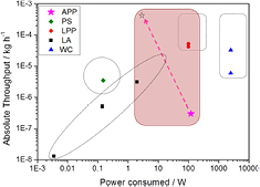
Figure 7. Diagram reporting absolute throughput versus power consumption as described in the text. For the atmospheric pressure plasmas, the dashed arrow indicates the scale-up potential of this technique by increasing reactor size and improving the precursor yield (acronyms are also described in the text).
Download figure:
Standard image High-resolution imageThroughput density (kg h−1 m−2).
A crucial feature required for integration of Si QDs into devices is the possibility of depositing on substrates and forming NPs thin films. In this sense, LPP and APPs are one step ahead of the other methods since they can achieve direct deposition. However, the area that can be coated is physically limited by the geometry of the plasma reactor. Throughput density can therefore provide a better comparison of scalable (in size) reactors. The comparison is limited here to APPs and LPPs as the other synthesis methods cannot offer QDs deposition directly on substrates. Assuming that both APPs and LPPs can be scaled up to comparable sizes, it would make sense to define a throughput per unit area of the deposition surface. The throughput density has been therefore calculated from the absolute throughput divided by the surface area that the reactor can cover, which was 32–80 cm2 and 2.5 mm2 for the LPP [44, 70] and the APP (this work and [39]) respectively. By comparing these figures, it can be seen how the throughput density of the APP is closer and comparable to the throughput density of the LPP (see table 1).
Cost ($ kg−1).
The cost involved in the synthesis of QDs is probably one of the most difficult parameters to evaluate. Therefore, as before, we have limited our discussion to comments on a few relevant parameters (i.e. raw materials, waste, energy consumption and up-front costs) from which a general cost trend can be assumed. Costs may vary drastically depending on QDs qualitative parameters and application requirements and it is clear that a full cost analysis and life cycle assessment, including the environmental footprint would be very beneficial.
The use of crystalline wafers for PS and LAL introduces intrinsically high raw materials costs with non-negligible waste. While LAL could in principle produce Si QDs from amorphous silicon, which would reduce the raw material costs, this has not been reported yet. Silane, used for LPPs and APPs, is generally more expensive than SiCl4 [82] although they can be both considered cheaper than chemical compounds needed for WC; also, very high yields with very low waste materials is a key advantage of APPs/LPPs compared to PS, LA and WC. Electrochemical etching and WC necessarily make also use of a range of chemicals and solvents that significantly add to the synthesis costs, especially for WC methods. Energy consumed for the synthesis process per unit weight of Si QDs (J kg−1) can represent a large fraction of the costs and this can be determined by the power consumed divided by the absolute throughput. The power for a typical etching process results to be ~0.15 W for about ~3 h etching with some variations depending on the size of the QDs [69]; depending on the etching conditions the power may also be higher, which however allows for shorter processing times. Power consumed in WC methods is well above 1 kW as typical ovens consume 2.5 kW to reach ~1000 °C with processing times that vary from a few hours to days [67, 68]. Low temperature WC methods are in principle possible because the energy required for the reactions to take place is chemically stored in the precursor or other chemical compound used in the synthesis process; for instance in order to prepare Mg2Si, which is used as precursor for the synthesis at room temperature, heating at 750 °C for 3 d is required [64]. Power consumption for plasma methods (both LPPs and APPs) are somewhat simpler to interpret because of the one-step process where the power used to sustain the plasma (~100 W [39, 44, 70]) is all that needs to be taken into account. It should be noted however that the literature generally refers to the applied power, which can be drastically reduced (by one order of magnitude) if customized power supply systems were to be built. Similarly to PS, synthesis of Si QDs by LAL is also very energy efficient with <5 W power consumption either as stated from the literature or calculated from the fluence, wavelength and repetition rate of the laser [71, 72, 74]. The up-front costs of equipment and maintenance are high for LAL and LPPs compared to the other techniques, due to the cost of lasers, power supplies and vacuum systems. WC and PS can be implemented with the cheapest investments while APPs probably sits in between as costs due to vacuum system are not required. Although a quantitative analysis would be required, if the potential scalability is taken into consideration, APPs appears to offer competitive advantages with the possibility of low-cost precursors, moderate up-front costs and moderate energy consumption.
The analysis conducted above has provided some figures of merit and an approximate comparison of different methodologies for the synthesis of QDs. It is clear that APPs can provide a range of benefits for a wide range of Si QDs applications both in qualitative as well as in quantitative terms. In particular direct deposition and/or direct integration in devices could represent one of the major competitive advantages due to relatively low costs and high versatility offered by APPs. Nevertheless, it has been highlighted that further research in all synthesis methods is required to bring the synthesis of Si QDs closer to a manufacturing reality.
2.4. A 0D theoretical model for crystallization at atmospheric pressure
Because low-pressure plasmas synthesis represents an important reference process, it may be relevant to highlight some of the differences between low pressure and atmospheric pressure processes. Synthesis of Si QDs and their crystallization in low pressure plasmas have been shown to originate from two coupled but different mechanisms, the first initiated from the polymerization of silane radicals (SiHx) and the second due to selective heating of the growing NPs due to ion/electron currents and surface recombination/exothermic chemical processes [40]. Added concentrations of hydrogen have been also shown to provide an essential contribution to both the nucleation/growth as well as to NP heating [40].
At atmospheric pressure similar processes are expected, however their relative contributions may impact in different ways. For example, it has been shown that additional hydrogen is not essential to the synthesis and crystallization of Si QDs at atmospheric pressure [39]. Effective dissociation of the precursor depends on the plasma reactivity which is influenced by the highly energetic electrons in the plasma. The energy distribution of electrons in atmospheric pressure microplasmas is much further from a Maxwellian distribution, compared to a low-pressure plasma, and a considerable population of highly energetic electrons is expected in this type of plasmas, which might explain the effective precursor dissociation for growth of nanomaterials at atmospheric pressure [24, 25].
We have developed a simple model that describes NPs heating in an atmospheric pressure plasma in argon background and without any added hydrogen [39]; in the model, NPs heating has been determined from ion/electron collisions, recombination and conduction cooling [39]. In order to account for effects of the atmospheric pressure, the expression for the ion current has been modified to accommodate a more collisional regime [39]. Comparison of NP temperature calculated from the well-known orbital motion limited (OML) theory and the temperature obtained from the collision-corrected model (CCM) show that NPs can reach much higher temperatures due to the ion–neutral collisions around the NP [39]. In particular for Si QDs, the OML-derived temperature is 600–610 K while the CCM-derived temperature is 780–790 K at given conditions [39]. This temperature difference is very important considering that crystallization of QDs is expected to take place, for instance, at 773 K for a 4 nm diameter QD [83, 85].
Although further experimental evidence and more theoretical developments are required, the results available point out that at atmospheric pressure, silicon atomization and Si atoms direct nucleation may form the initial steps of Si NPs growth; this is possible at atmospheric pressure due to more efficient and full dissociation of the silane precursor. At the same time, NPs heating up to crystallization temperatures can take place thanks to the collisional regime even without the contribution of added hydrogen; note that added hydrogen can increase the NP temperature by surface exothermic reactions as well as by increasing the overall background gas temperature.
The model input parameters were obtained from experimental measurements in our previous work [39], however by varying these parameters it is possible to map, for example, crystallization regimes that depend on the gas temperature as well as on the electron density. This assumes a constant electron temperature (Te = 1 eV) and it should be noted that the impact of electron temperature on NPs temperature is weaker than the effect of the electron density.
In figure 8 we report the plasma conditions (gas temperature and electron density) for which a 4 nm diameter Si QDs reaches its crystallization temperature, estimated to be 773 K. The results presented in figure 8 clearly show that QDs are heated above the background gas temperature due to the balance of energy delivered via ion and electron kinetic energy and ion–electron recombination against losses due to conduction to the surrounding gas. Therefore at higher electron (and ion) densities, crystallisation occurs at lower gas temperatures. Typical gas temperature and electron density ranges of atmospheric pressure plasmas (can vary from 300 K to thermal [36, 84–86] and from 1011 to 1015 cm−3 [39, 85, 86], respectively, which cover both the crystallization and non-crystallization conditions (figure 8). This theoretical result seems therefore to explain why experimentally APPs can crystallize QDs in an argon background and the contribution of added hydrogen either to increase the gas temperature (i.e. by enlarging the blue area in figure 8) or to invoke surface chemistry driven heating mechanisms (i.e. down-shifting the blue dots/line in figure 8) is not required. While APPs have similarities with LPPs, there seem to be a range of differentiating factors and mechanisms that may provide APPs with differing and unique synthesis characteristics at least for some materials and some applications (e.g. a more sensitive parameter space).

Figure 8. Diagram reporting the gas temperature and electron density required to reach 773 K (crystallization temperature) in a 4 nm diameter quantum dot (QD); the calculations were performed within the collision-corrected model (CCM; blue squares). The blue area described the range of parameters achievable with atmospheric pressure plasmas (APPs). Linear trend (blue dashed line) is also included. The red dots display the calculation within the framework of orbital motion limited (OML) theory [39].
Download figure:
Standard image High-resolution image3. Advances in surface engineering and composition tuning of Si-based quantum dots
3.1. Tailoring silicon quantum dots band energy structure by post-treatment and surface engineering
Silicon QDs, due to their strong confinement regime, can be manipulated to tailor their energy structure and transition dynamics: for instance modifying the QDs surface it is possible to vary absorption, carrier life-time, stability and overall optoelectronic properties [16, 87, 88]. Furthermore additional strategies to reduce defects and dangling bonds of Si QDs for the fabrication of device grade thin films are required. In order to have access to surface characteristics, synthesis methods that can produce surfactant-free and free-standing QDs are required and a range of surface engineering approaches are possible (see [16] and references therein). In particular, microplasma-liquid interactions have recently revealed interesting opportunities for surface engineering of Si QDs directly in colloids. In these cases, the microplasma is generated above the colloid allowing for direct plasma-liquid interactions (figure 9); chemical reactions initiated at the plasma-liquid interface are believed to induce surface chemistries that are not achievable with other techniques [89, 90].

Figure 9. Diagram describing the arrangement of plasma-liquid systems for surface engineering of silicon nanocrystals (Si-ncs); (a) a direct current (dc) microplasma directly coupled to the colloid; (b) an ultra-high frequency (uhf) microplasma used as 'jet' on a colloid. Adapted with permission from [16], Copyright 2013 RCS.
Download figure:
Standard image High-resolution imageFigure 9 depicts possible arrangements of microplasmas interacting with colloids of Si QDs where either a dc microplasma or an ultra-high frequency (UHF) microplasma (450 MHz) have been used [16]. The dc microplasma (figure 9(a)) is directly coupled (0.5–2 mm distance between the liquid and the metal capillary) to the colloid and the voltage (<2 kV) is applied to the counter electrode immersed in the conductive liquid (e.g. water-based). The UHF microplasma (figure 9(b)) does not require a return path for the current allowing for the treatment of Si QDs in non-conductive media (e.g. toluene, chlorobenzene etc); the plasma is formed within a quartz capillary and jetted out onto the colloid from a 1–2 mm distance. Full experimental details on both dc and UHF microplasma treatments can be found elsewhere [16, 69]. A range of chemistries are possible via these schemes and indirectly they all may affect the outcome of the surface engineering [99]. Nonetheless, it is believed that for the surface engineering of the Si QDs, electrons injected from the plasma greatly and mainly contribute to induce a chain of chemical reactions in the liquid phase which is hardly achievable by any other technique (e.g. standard wet chemistry, electrochemistry or radiolysis). The use of these simple microplasma systems to modify Si QDs surface characteristics directly in colloids has produced a range of useful results: for instance it has been possible to improve Si QDs optical properties [89, 99], increase the QDs long-term stability in various liquids [69, 90] and the synthesis of novel Si QDs/polymer nanocomposites has been achieved [101]. The same method is also being applied for the synthesis and surface engineering of a wide range of other materials (e.g. [99, 102]). While the scaling up of this set-up has not been addressed yet, microplasma-liquid systems represent useful tools to investigate unique surface effects of nanoscale objects leading to important scientific advancements.
As an example, here we will review briefly some results produced by applying an atmospheric pressure dc microplasma process (figure 9(a)) to water-based Si QDs colloids and we will focus on surface engineering of Si QDs produced by electrochemical etching (i.e. from PS); details of the electrochemical etching procedure are similar to our previous reports (80 mL of 1:4 HF/ethanol solution, 30 mA etching current, 90 min etching time, p-type silicon wafer), which produces Si QDs with a ~2 nm average diameter (e.g. [90, 101, 103]). Prior to the Si QDs dispersion in water, 3 mg Si QDs were wetted by adding a few drops (<100 μL) of ethanol and then exposed to air for ~3 h until ethanol had fully evaporated. The water/Si QDs colloid was then formed by adding 5 mL of distilled water; the colloids used for the analysis and surface engineering were taken after 15 min sedimentation, so that large aggregates were removed.
Si QDs obtained from PS are generally H-terminated with possible surface dimers as well as dangling bonds [43, 91, 92]; this is evident from the corresponding Fourier transform infra-red spectrum (figure 10(a), top blue line) which exhibits different types of Si–Hx terminations (600–650 cm−1, ~900 cm−1, ~2100 cm−1) and only very limited oxidation (~1070 cm−1). When water or water vapour come in contact with Si QDs, dimers and dangling bonds are quickly reacted to form silicon oxide; furthermore oxidation also proceed through reaction at the Si–Si back-bonds of the Si–H terminations and more slowly hydrogen terminations are also replaced with Si–OH. Condensation of Si–OH will then contribute to the formation of a continuous oxide shell with a range of possible coordination arrangements (Si–O–Si, Si=O etc) [93]. The Fourier transform infra-red (FTIR) spectrum of Si QDs aged in water for 1 d is shown in figure 10(a) (red line in the middle) which confirms a drastic decrease in Si–Hx absorption (600–650 cm−1, ~900 cm−1, ~2100 cm−1) and the appearance of surface oxide-related peaks (~1070 cm−1) as well as oxide growth on silicon back-bonds (OySi–Hx within the range 850–950 cm−1).
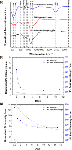
Figure 10. (a) Fourier transform infra-red (FTIR) spectra of dry Si quantum dots (QDs) from porous silicon (top, blue), Si QDs stored in water for one day and surface engineered Si QDs also stored in water for one day. (b) Photoluminescence (PL) peak relative intensity (open black circles) and corresponding wavelengths (full blue squares) for Si QDs stored in water versus days. (c) PL peak relative intensity (open black circles) and corresponding wavelengths (full blue squares) for surface engineered Si QDs stored in water versus days; the break in the x-axis separate the Si QDs PL before and after surface engineering by microplasma.
Download figure:
Standard image High-resolution imageThe initial oxide growth has impact on the optical properties whereby any dangling bonds or strained Si-bonds/dimers are removed and allow increasing the radiative transitions of carriers that are trapped in oxide-related surface localized states. This can be generally observed in the photoluminescence (PL) of Si QDs dispersed in water colloids for instance, where the PL intensity is observed to increase within the first few hours [90]. Nonetheless, after a few hours, water exposure and continued oxidation necessarily leaves behind further defects and strained bonds that are susceptible to further water cleavage [94] and allow for the oxidation to progress inward. While controlled oxygen-based passivation that is restricted to the outermost layers can improve optoelectronic properties by reducing surface defects, inward oxide growth increases defects density at the oxide localized states and therefore provides both non-radiative recombination paths for electron–hole pairs with consequent decreased PL and recombining centres that degrade carrier transport. Figure 10(b) confirms the progressive loss of PL emission for Si QDs that were stored in water for a number of days; the blue shift of the peak wavelength is associated with a decrease in size of the Si QD core due to the formation of an oxide shell.
It follows that Si QDs degradation in water represents a limitation for Si QDs and many studies have therefore shown that, for instance, the PL stability can be somewhat improved either by capping Si QDs with bio-compatible polymers [95–97] or with an ultrathin-oxide layer [98]. The dc microplasma applied to Si QDs/water colloids allows controlling the surface properties of the Si QDs, prevent extensive oxidation and allows for stable Si QDs colloids with improved PL emission. In this case we applied a dc microplasma treatment (figure 9(b)) to our Si QD colloids for 60 min; a 0.5 mA constant current was applied to sustain the microplasma (0.25 sccm He through a Ni capillary with 0.25/0.5 mm internal/external diameter) and the distance between the capillary and the surface of the colloid was ~1 mm.
Figure 10(c) shows the PL characteristics in terms of intensity and wavelength of the spectral emission peak for Si QDs that have been surface engineered with the dc-microplasma and then stored in water for a number of days. The break in the x-axis of figure 10(c) separates the PL measurements before and after microplasma processing, which displays a dramatic increase (×13) in PL intensity soon after the microplasma process. Although the PL intensity shows also in this case a decreasing trend with time, it is observed that after 15 d, the Si QDs still present a strong PL peak intensity which is about five times higher than the initial PL emission, while the Si QDs that were not surface engineered (figure 10(b)) have lost all of the PL emission with respect to the initial value. The wavelength blue shift in figure 10(c) also confirms that the oxidation process is somewhat halted for surface engineered Si QDs as the peak wavelength tends to stabilize at ~610 nm compared to ~570 nm for untreated Si QDs (figure 10(b)). It should be noted that the initial wavelengths (days = 0) recorded for figures 10(b) and (c) should in principle have the same value; however the ~36 nm difference is due to the very time-sensitive nature of the oxidation process as demonstrated by the very sharp exponential decay in figure 10(b), where a wavelength difference of ~36 nm can be easily observed for PL measurements taken within the first day. As this study is concerned with the stability of the Si QDs over much longer periods, time-dependent measurements with hour or minute accuracy were not carried out on this occasion.
While the PL measurements show clear differences in the optical behaviour of the Si QDs, the FTIR spectrum of surface engineered Si QDs (figure 10(a), bottom black line) presents only very subtle differences from the Si QDs aged in water (figure 10(a), middle red line). In particular, Si–Hx bonds disappearance is more pronounced in the processed Si QDs (at ~2100 cm−1, just below 1000 cm−1 and within 600–650 cm−1), the O2Si–H peak (~950 cm−1) appears to be stronger for surface engineered Si QDs and finally the ~1070 cm−1 oxide peak exhibits a sharper separation from its shoulder at higher wavelength. These small but important differences are evidence of different Si–O bond arrangements, possibly pointing at a more regular and stoichiometric oxide for the microplasma-treated Si QDs. The oxidation of surface engineered Si QDs is expected to be initiated by electron-induced reactions at the plasma-liquid interface, which are likely to produce high concentrations of OH/OH−. These reactive species can quickly replace the H-terminated surfaces of Si QDs; Si–OH condensation [100] then forms a thin oxide layer that can quickly prevent inward oxidation [69]. In water, without the plasma treatment, Si QDs would be exposed to back-bond oxidation promoting the inward oxidation and the consequent loss of PL emission.
3.2. Composition tuning: synthesis of alloyed silicon-based quantum dots
Alloying silicon with another element offers the possibility of varying the bandgap of Si QDs, with the opportunity of tuning the band energy structure for specific applications. Furthermore silicon alloying can also produce the material transition from indirect to direct behaviour [21, 104, 105]. The synthesis of Si-alloys presents important challenges due to the difficulties of accessing thermodynamically unstable phases and due to the low solubility of the alloying elements in silicon. For instance, the large size difference between the Si and Sn atoms can result in the thermodynamic instability of the Si–Sn alloy due to lattice mismatch and consequent strain energy. However, Si–Sn QDs, due to strains introduced by the nanoscale dimensions, experience a smaller energy difference between the segregated phase and the alloyed phase making the formation of Si–Sn alloys at the nanoscale more favourable [105]. The synthesis of Si–Ge NPs has been already demonstrated by LPP [40, 106] and other methods [107, 108], which demonstrates that for many non-equilibrium processes such as plasmas, the synthesis of nanoscale structures based on alloyed silicon systems is an obvious step forward from Si QDs.
Si–C alloys can produce materials with increased bandgap compared to elemental Si QDs; silicon carbide also offers high thermal and chemical stability. Luminescent SiC QDs are attractive for a range of applications including bio-imaging [109, 110]. However, their synthesis with control over their properties is still challenging. Electrochemical etching of SiC wafers or etching of SiC powder has been mostly used for producing luminescent SiC NPs. For example, Fan et al has reported synthesis of luminescent NPs from etching wafers of different polytypes of SiC [111, 112]. Similar approaches have been employed for etching of SiC powder by Yong Li et al for producing SiC NPs with a 4.4 nm diameter [113]. Device-grade NPs demands developing a simple and environmentally friendly synthesis method that could be easily scaled-up.
We have previously demonstrated the synthesis capability of SiC QDs with our atmospheric pressure plasma based on the two-ring configuration and using tetramethylsilane (TMS) as precursor; the crystalline nature and chemical composition was supported by our TEM (including diffraction patterns) and XPS analysis [114]. Therefore, most recently we have replicated the same synthesis approach with TMS precursor utilizing the scalable configuration (figure 2) [36]. Again, TMS is supplied by flowing argon gas through a bubbler, which was used to vary TMS concentration and the resulting QD diameter within the range 2–5 nm. Figure 11 shows a typical TEM image and high resolution TEM image (inset) of the SiC QDs (~3.7 nm average diameter) produced with 2.4 sccm argon flow through the TMS bubbler and 1000 sccm background argon gas; the applied power was 100 W. Detailed material characterization that included FTIR, XPS and TEM analysis has demonstrated the crystallinity of the alloyed Si–C system [36, 37]. The fringes spacing for the QDs was determined from high resolution TEM image (0.22 nm) and corresponds to the (2 0 0) planes of 3C–SiC (e.g. see inset of figure 11). The FTIR and XPS chemical analyses of the samples confirm that the QDs have Si–C bonds consistent with the alloyed Si–C system ([36, 37] and supporting information) (stacks.iop.org/JPhysD/48/314002/mmedia).
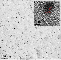
Figure 11. (a) Transmission electron microscope (TEM) image of SiC quantum dots prepared in the scalable plasma reactor for a bubbler flow rate of 2.4 sccm in 1000 sccm argon flow with 100 W applied power. The fringes spacing in the high resolution TEM image in the inset is 0.22 nm and corresponds to the (2 0 0) plane of β-SiC. The average size for this sample was ~3.7 nm.
Download figure:
Standard image High-resolution imageBoth theoretical and experimental work on bulk Si1−xSnx materials has demonstrated a direct bandgap that is progressively reduced for a sufficiently high concentration of Sn due to the direct zero-gap nature of bulk α-Sn [105]. The extension of these bulk studies to quantum confined systems, to bring bandgap tuning (through composition and size) is therefore of great scientific interest. Manipulating bandgap and direct/indirect nature of the QDs would allow fine tuning of absorption, absorption edges etc. For the synthesis of Si–Sn QDs we have used a laser-produced plasma in liquid [21]. The laser was focused on an amorphous Si–Sn target immersed in water. Within the short pulse duration, a high-temperature, high-intensity, and high-pressure plasma plume of Si and Sn atoms is produced over the laser spot [115]. Subsequently, the plasma plume expands and results most likely in the formation of Si nuclei, due to the low Sn concentration. These nuclei continue to grow until nearby silicon clusters and Sn atoms are completely incorporated and consumed, with consequent termination of the growth process [116]. At quantum confinement sizes (<10 nm), the energy barrier for alloy formation is smaller than in bulk materials because a large fraction of the Sn and Si atoms are in high energy states due to a range of factors such as a re-organized structure of the core, increased surface curvature and an overall higher surface energy due to the increasing surface-to-volume ratio. Therefore Si–Sn alloying is facilitated at the nanoscale and phase segregation may be avoided also for Si–Sn QDs with even high Sn concentration.
We have explored the synthesis of Si–Sn QDs starting from amorphous Si–Sn targets at varying tin concentrations. Previously we reported the formation of SiSn QDs from targets with 5% Sn concentration where alloying was supported by TEM analysis (including diffraction patterns), energy-dispersive x-ray spectroscopy and Raman analysis [21]. A clear wavelength red-shift of the PL maximum was observed corroborating the bandgap reduction [21]. Also for these QDs, the surface is expected to play a role in determining the optical properties and surface engineering by microplasma-induced liquid chemistry was a necessary step to observe the PL shift [21]. The PL maximum was located in the visible range of the spectrum at around 660 nm (1.88 eV). Figure 12 reports a TEM image of Si–Sn QDs produced with a 10 ns laser (KrF, 245 nm, 20 Hz, 10 ns, ~23.5 mJ cm−2) focused on a 1.5 mm spot on the target in ethanol; the tin concentration was in this case 10% [36]. Detailed high resolution TEM analysis has shown that the fringes with spacing ~0.2 and ~0.25 nm were found and can be attributed respectively to the planes (2 2 0) and (2 1 1) of a face-centred cubic unit with the cell parameter 0.608 nm (e.g. inset of figure 12 and [36]). It should be noted that the unit cell dimensions of cubic Si and Sn are equal to 0.5431 and 0.6473 nm, respectively. The fact that the cell parameter (0.608 nm) falls between these two values suggests that the synthesised QDs are alloys of Si and Sn. However, further analysis is required to confirm alloying throughout the samples; however these results are quite encouraging and consistent with our previous work at similar conditions [21]. As expected the laser-based process produces QDs and NPs with a wide size distribution; nonetheless, laser ablation in liquid appears to be extremely effective in QDs synthesis at least for fundamental materials research and to demonstrate materials feasibility at quantum confinement regimes.
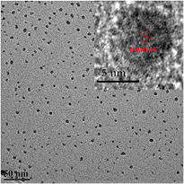
Figure 12. Transmission electron microscopy (TEM) image of SiSn quantum dots from pulses (10 ns) of an excimer laser (KrF, 245 nm, 20 Hz, 10 ns, ~23.5 mJ cm−2) focused on a 1.5 mm spot on the target in ethanol. The target was an amorphous silicon target with 10% tin. The inset reports a high resolution TEM image demonstrating the crystallinity of the quantum dots and corresponding lattice spacing.
Download figure:
Standard image High-resolution image
Si-alloying with group IV elements has been therefore demonstrated both with gas-phase atmospheric pressure plasmas as well as with laser-produced plasmas in liquids. Si-based alloyed QDs have great potential for many applications due to their wide range of tunable properties and limited environmental footprint which makes them highly attractive.
4. Conclusions
Plasma-based processes represent very well matched methodologies for the synthesis of silicon-based QDs and NPs. Plasmas enable both gas-phase and liquid-phase chemistries not available through other synthesis methods offering parallel but distinct control mechanisms to achieve tailored nanomaterials properties. Furthermore plasmas are sufficiently versatile and low-cost to offer clear advantages over other methods for group IV materials. Low-pressure plasmas have made significant progress for Si QDs and NPs in the past years. The most recent developments are demonstrating great capabilities of plasmas also at atmospheric pressure; it is apparent that atmospheric pressure plasmas can deliver high quality Si QDs and in general can produce nanomaterials to meet demanding application requirements.
Scaling up nanomaterials synthesis by atmospheric pressure plasmas is yet to be fully demonstrated although significant progress has been made. It should be noted however that large scale nanomanufacturing is still a challenge for most synthesis methods with respect to Si-based QDs; in this context, atmospheric pressure plasmas are not far behind than other technologies and present great scale-up potential. Furthermore, Si-based QDs, like many other advanced materials, are still at the research stage whereby 'lab-grade' synthesis methods are expected to prioritize the qualitative aspects rather than immediate industrial scale manufacturing. Or in other words, it is important that Si-based QDs first demonstrate their successful implementation in application devices before scaling up can be fully justified.
Possibly, one of the most interesting aspects is that atmospheric pressure plasmas exhibit peculiar properties that are different from low-pressure plasmas and other techniques. It is therefore important to view the development of atmospheric pressure plasmas as a complementary technology that could allow exploring new synthesis avenues and lead to novel materials or materials compounds with beneficial properties.
Acknowledgments
This work was supported by the Leverhulme International Network (IN-2012–136), and EPSRC (EP/K022237/1). SA thanks the financial support of the University of Ulster Vice-Chancellor Studentship. DM wishes to acknowledge the work of Dr Andrew Wagner and the support of Applied Materials Inc. and the Microelectronic Engineering Department at the Rochester Institute of Technology (NY, USA) for the development of the plasma reactors in figure 4. The authors also acknowledge Dr Ni Chengsheng for the tilted image inset of figure 3.