
Abstract
P-type cuprous oxide films were prepared by magnetron sputtering with different crystallization degrees from columnar polycrystalline to amorphous phase. The film with amorphous structure possesses a hole concentration of 1.92 × 1019 cm−3, even comparable to those of MIII- doped Cu2O crystalline films and two orders of magnitude higher compared to the well crystallized Cu2O, 6.51 × 1017 cm−3. Meanwhile, Hall mobility of the amorphous film is one order of magnitude larger with respect to those of the crystalline counterparts. Combining high-resolution transmission electron microscopy observations with x-ray photoelectron spectroscopy analysis, it is revealed that the localization of holes at the oxygen 2p band can be weakened by suppressing crystallization for the films, which is believed to be attributed to the asymmetric characterizations of Cu–O chemical bonds caused by topological disorder atomic arrangement inherent to amorphous structure.
Export citation and abstract BibTeX RIS
1. Introduction
Transparent conductive oxides (TCOs) continue to attract a great deal of attention due to their desirable combination of optical transparency in the visible region and electrical conduction. These properties are essential for the application of solar cells, flat-panel displays and other optoelectronic devices where transparent electrodes are needed to convey electric and optical signals [1–3]. However, most of these materials are n-type electrical conductors and consequently their application as semiconductors is rather restricted [4]. In this respect, there has recently been a particular interest in materials science for studying transparent p-type conductors [5–7]. A combination of the p-type with the well-developed n-type transparent conductor in the configuration of pn junction is a crucial step towards expanding utilization of TCOs as transparent semiconductors.
Up to date, p-type oxides can usually be achieved by improving the conductivity of a wide band-gap semiconductor by introduction of cation deficiency caused by doping [8, 9]. Since the first report on p-type conductivity in a highly transparent CuAlO2 film in 1997 [10], several other ternary oxides by doping MIII trivalent ions or MII divalent ions in Cu2O have been extensively investigated [5, 11], in an attempt to develop p-type semiconductors with a wide band-gap as well as electrical conductivity comparable to those of the existing and widely used n-type semiconductor films. The alloying of the third element with Cu2O is believed to be favourable for reducing the Cu–Cu interaction by destroying the O–Cu–O network structure therein. For example, doping the ions (MIII) such as Al3+, In3+, Fe3+ and even B3+ into Cu2O leads to the formation of CuMO2, generally accompanied by a great reduction of the Cu–Cu interaction [5, 6, 10]. However, the MIII- doped Cu2O oxides usually exhibit complex structure and their compositions are difficult to control. In addition, an increase of hole concentration is usually at the expense of sacrificing the high mobility attributed to high-quality crystalline structure [10].
It is a widely acknowledged fact that the p-type conduction feature of Cu2O is attributed to a peculiar cuprite cubic structure belonging to space group Pn3m, which is characterized by the situation of the oxygen atoms at the bcc lattice site. As such, each of the O atoms is surrounded by four Cu atoms to construct a tetrahedral structure, giving rise to formation of O–Cu–O chemical bond [12]. Since the holes often exist at the top of valence band state in the Cu2O, a slight variation in the structure including atomic arrangement can be expected to change the O–Cu–O chemical state as well as O 2p state. In fact, the p-type electrical resistivity of Cu2O film has been reported to vary over a large range of 10–103 Ω cm with different research groups, corresponding to a large diversity in hole concentrations of 1015–1018 cm−3 and in mobility of 101–10−2 cm2 V−1 s−1 as well [13–15]. It can be anticipated that the inconsistency may come from subtle variations in the microscopic structure which are hardly avoided during preparation processes on different fabrication apparatus. Therefore, it is of scientific interest and technological significance to obtain an insight into the understanding of the microstructure dependent properties of the p-type films.
In this work, we report our recent observations that the p-type conductivity of Cu2O film varies greatly with crystallization degree. The hole concentration and mobility are simultaneously improved by reducing the crystallization degree; especially for an amorphous Cu2O film, its hole concentration reaches up to 1.92 × 1019 cm−3. The underlying mechanism is discussed in detail in combination with the crystallinity effect on chemical bond states.
2. Experimental section
Cu2O films were deposited at room temperature by reactive magnetron sputtering method. Glass and quartz substrates were chosen to combine with deposition conditions (as summarized in table 1) for growth of the films with different crystallization degrees and they were ultrasonically cleaned for deposition. Copper target (purity ⩾99.9%) with 60 mm in diameter and 3 mm in thickness was applied. The chamber was evacuated to a base pressure of 8 × 10⁻⁴ Pa prior to the deposition which was performed in a mixed atmosphere of oxygen and argon with purity of 99.99%. Impulse and radio frequency (rf) power supplies were applied to adjust the crystallization extent during the deposition process. Here, the impulse power supply refers to a medium frequency power supply with square wave alternating current. Structure of the films was studied using x-ray diffraction (XRD, D8 Advance Bruker AXS) under the conditions: voltage 40 kV, current 40 mA and Cu Kα radiation. The angle error and peak broadening caused by instrument bias were calibrated by using an α-Al2O3 standard sample (SRM-1976a). Film microstructures were observed by high-resolution transmission electron microscopy (HRTEM, JOEL-2100F) along with field-emission scanning electronic microscope (FESEM, Hitachi-S4800). X-ray photoelectron spectroscopy along with Auger electron spectroscopy (XPS and AES, AXIS UTLTRADLD SHIMADZU multifunctional x-ray photoelectron spectroscope) were applied to study Cu 2p and O 1s core levels of the Cu2O films. Electrical properties were measured at room temperature using Hall-effect measurement system (ACCENT HL5500PC).
Table 1. Deposition parameters for the preparation of the Cu2O films with different crystallization degrees.
| Sample | Power supply | Substrate | TSD (mm) | PAr (Pa) |
 (Pa) (Pa) |
DP (Pa) | Power (W) | Thickness (nm) |
|---|---|---|---|---|---|---|---|---|
| Cu2O_c1 | Impulse | glass | 50 | 1.3 | 0.3 | 1.6 | 195 | 620 |
| Cu2O_c2 | Impulse | glass | 50 | 1.3 | 0.3 | 1.6 | 180 | 570 |
| Cu2O_c3 | Impulse | glass | 60 | 1.4 | 0.4 | 1.8 | 120 | 350 |
| Cu2O_α | rf | quartz | 60 | 1.5 | 0.4 | 1.9 | 80 | 210 |
Note: TSD: target to substrate distance; PAr: argon partial pressure;
: oxygen partial pressure and DP: sputtering pressure.
3. Results and discussion
3.1. Microstructure characterizations
As shown in figure 1, several diffraction peaks are clearly seen in the XRD profiles for Cu2O_c1, Cu2O_c2 and Cu2O_c3 films, indicating that they are crystalline phase with random orientation. The diffraction peaks are identified as reflections of the crystal planes resulting from cuprite cubic structure [16]. The peak intensities decrease in the order of Cu2O_c1, Cu2O_c2 and Cu2O_c3, and finally disappear for Cu2O_α. As listed in the inserted table, Cu2O_c3 shows the largest values of full-width at half-maximum (FWHM) of (1 1 1) and (2 0 0) peaks in contrast to the smallest ones for Cu2O_c1. The results indicate that the crystallization degrees for the Cu2O films decrease in the order of Cu2O_c1, Cu2O_c2, Cu2O_c3 [17], while the Cu2O_α is in an amorphous state.
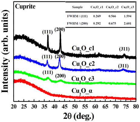
Figure 1. XRD profiles for the Cu2O_c1, Cu2O_c2, Cu2O_c3 and Cu2O_α films prepared with the deposition parameters shown in table 1. Inserted are the values of FWHM of (1 1 1) and (2 0 0) peaks for Cu2O_c1, Cu2O_c2 and Cu2O_c3.
Download figure:
Standard image High-resolution imageThe cross-sectional microstructure of the films was examined by FESEM, as shown in figures 2(a)–(d). The Cu2O_c1 film demonstrates a clear columnar structure with growth direction along cross-section. By contrast, the columnar image has an ambiguous boundary for Cu2O_c2 and cannot be detected for Cu2O_c3, consistent with the different crystallization degrees indicated from the XRD analysis. For the Cu2O_α, as expected, no crystalline phase is seen throughout the whole film. The film thicknesses estimated from the observation are consistent with the nominal ones derived from the corresponding deposition rate and time. Furthermore, HRTEM images for the films along with selected area electron diffractions (SAED) inserted are shown in figures 2(e)–(h). The Cu2O_c1 film consists of nanocrystalline with the grain size of about 15–20 nm, while Cu2O_c2 and Cu2O_c3 films are characterized by two-phase structure with nanograins embedded in amorphous phase. The gain size varies in the range of 8–12 nm and of 2–4 nm for Cu2O_c2 and Cu2O_c3, respectively. As is evident from the SAEDs, the nanograins are randomly oriented and identified as cuprite cubic structure. While for the Cu2O_α film, the SAED shows a halo-like character, confirming that the film is highly disordered in terms of long-range atomic arrangement.
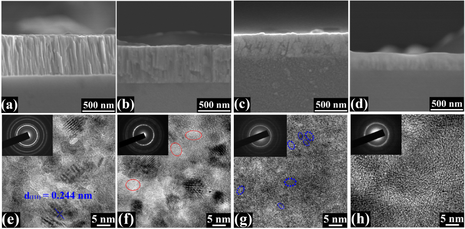
Figure 2. FESEM cross-sectional micrographs for the films: (a) the Cu2O_c1, (b) the Cu2O_c2, (c) the Cu2O_c3 and (d) the Cu2O_α films, respectively. HRTEM images for the films along with their corresponding SAED patterns inserted: (e) Cu2O_c1, (f) Cu2O_c2, (g) Cu2O_c3 and (h) Cu2O_α. The estimated fringe spacing of 0.244 nm corresponds to the lattice distance of (1 1 1) plane stemming from cuprite structure. The marked red and blue circles indicate amorphous and crystallization areas, respectively.
Download figure:
Standard image High-resolution image3.2. Chemical bonding state of Cu
The Cu chemical binding states of the Cu2O_c1, Cu2O_c2, Cu2O_c3 and Cu2O_α films were determined based on XPS analysis. Figure 3(a) displays the wide-scan XPS spectra in the binding energy range of 0–1100 eV. The binding energies corresponding to the peaks were all calibrated by using the C 1s photoelectron binding energy of 284.8 eV. There is no evidence of any other element than Cu and O in the surface area of the films. Figure 3(b) demonstrates high-resolution spectra of Cu 2p core levels. Two peaks are clearly seen at 932.4 and 952.2 eV corresponding to the 2p3/2 and 2p1/2 for each of the films. In addition, no satellite peaks are detected around 941 and 944 eV in the Cu 2p spectra. The results indicate an absence of any chemical binding state of CuO in the films [18]. Nevertheless, the binding energies corresponding to the 2p3/2 of Cu2O and Cu are nearly the same, 932.4 and 932.2 eV, making it difficult to distinguish between them. Thus, high-resolution Auger electron spectra of Cu LMMa are displayed in figure 3(c). It is clearly seen that the peaks are located at the kinetic energies of 917.4 eV, 916.9 eV, 917.0 eV and 917.1 eV for the Cu2O_c1, Cu2O_c2, Cu2O_c3 and Cu2O_α films, respectively, which are nearly equal to the standard kinetic energy of Cu1+ LMMa, 917.2 eV [19]. The observation provides evidence that the crystalline Cu2O as well as the amorphous Cu2O_α films are all characterized by cuprous oxide phase, well in accordance with the XRD analysis as described above.
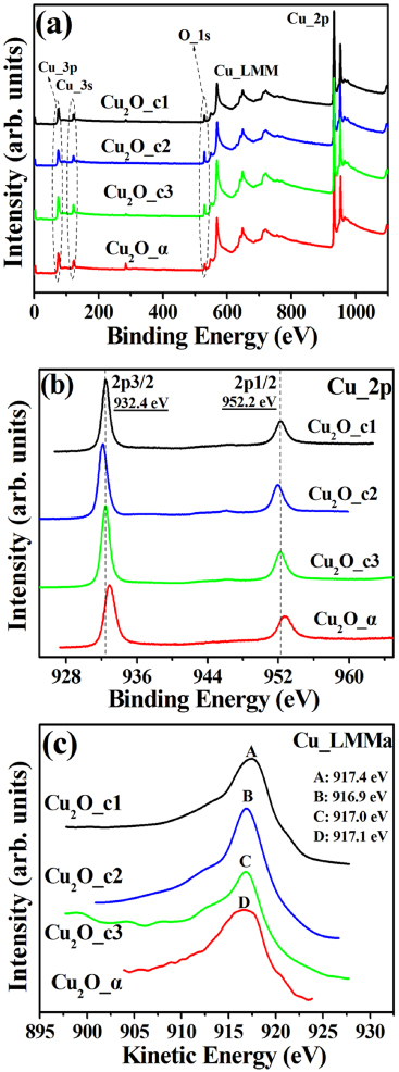
Figure 3. XPS and AES spectra for the films: (a) wide-scan spectra; (b) high-resolution Cu 2p core level curves in the binding energy range from 920 to 970 eV; (c) high-resolution Cu LMMa curves in the kinetic energy of 900–930 eV.
Download figure:
Standard image High-resolution image3.3. Electrical properties
3.3.1. Variations of hole concentration with crystallization degree.
Effect of the microstructure variations on electrical characterizations of the Cu2O films is investigated, as shown in figure 4. For the crystalline and amorphous films, Hall coefficients are all positive, showing that the films are, as expected, characteristic of p-type conductivity. However, the values of electrical resistivity are very different with the different samples. As shown in figure 4, resistivity of the Cu2O_c1 film is 564.6 Ω cm, much larger than 96.8 Ω cm for Cu2O_c2 and 6.04 Ω cm for Cu2O_c3. The amorphous film exhibits the smallest resistivity of 1.34 Ω cm. It is further seen from figure 4 that the hole concentration shows a monotonic increase with decreasing crystallization degree. The amorphous film has a hole concentration of 1.92 × 1019 cm−3, even comparable to those of MIII- doped Cu2O crystalline films [5], which is nearly two orders of magnitude higher than the well crystallized Cu2O_c1 film, 6.51 × 1017 cm−3. On the other hand, it should be mentioned that the presence of Cu vacancy is inclined to destroy stoichiometry of the oxide and consequently the molecular formula is basically represented by Cu2−yO, which may provide hole carriers on the basis of electrically neutral principle. However, the value of y is usually very small, less than 1.3 × 10⁻³, even if concentration of the Cu vacancy reaches the characteristic value of ∼1020 cm−3 beyond which the cuprite phase is destroyed at room temperature [9, 20]. The hole concentrations observed for the cuprous oxide presented in this work indicate that our samples remain stoichiometric even if it is in the amorphous state. However, the decrease of crystallinity for the films results in an increasing constituent of disorder atomic arrangements, which is very likely to destroy the symmetry of O–Cu–O bond demonstrated in well-crystallized Cu2O. In fact, amorphous structure has the asymmetry characterization of O–Cu–O chemical network due to its topological disorder structure [21, 22]. Theoretical study revealed that the asymmetry tends to decrease formation energy of Cu vacancy, which consequently reduces the correponding acceptor ionization energy [9, 23, 24] and in turn enhances hole carriers.
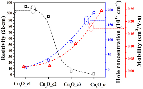
Figure 4. Resistivity (black), hole concentration (blue) and mobility (red) for the Cu2O films tested on Hall-effect measurement system at room temperature.
Download figure:
Standard image High-resolution image3.3.2. Effect of amorphization on hole mobility.
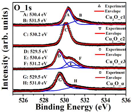
It is generally believed that an increase in carrier concentration tends to strengthen electron–electron scattering and consequently suppresses the hole mobility, which has been often seen in ZnO-based semiconductors [25, 26]. However, an intriguing result observed in this work is that the hole mobility is increased with increasing the hole concentration, as shown in figure 4. The mobility of the amorphous Cu2O_α is 0.234 cm2 V−1 s−1, a dozen times higher that of the crystalline Cu2O_c1, 0.017 cm2 V−1 s−1, although the Cu2O_α film possesses the largest hole concentration. High-resolution XPS spectra of O 1s core levels were examined to understand the dependence of hole mobility on the crystallization degree. As shown in figure 5, depending on the crystallization degree, two or three peaks can be deconvoluted from each of the O 1s core level spectra. For the Cu2O_c1 crystalline film, there are two peaks at 530.4 and 531.5 eV which are attributed to the lattice O of the crystalline structure and surface adsorption of O, respectively [18, 19]. In the case of the Cu2O_c2 film, only one peak is seen at 530.2 eV, corresponding to the lattice O. For the Cu2O_c3 film, a relatively strong peak at the lower energy of 529.5 eV is observed while those arising from lattice and adsorption O become weak to a large extent. Moreover, the peak at 529.5 eV is also observed for the amorphous Cu2O_α while the lattice O peak vanishes. The appearance of the lower binding energy peak indicates that covalent bonding constituent in O–Cu–O chemical bond is increased for the film with amorphous structure as compared to those of crystalline films. It is known that covalent bonding state possesses weakening localization of holes at oxygen 2p band as compared to ionized bonding [4, 27, 28], which is conducive to increasing carrier mobility. Therefore, the largest hole mobility for the amorphous Cu2O_α is attributed to the increase of covalent bonding constituent in the Cu–O bonding caused by suppression of crystallization degree in the cuprous oxide.
Figure 5. High-resolution XPS spectra of O 1s core levels for Cu2O_c1, Cu2O_c2, Cu2O_c3 and Cu2O_α in the binding energy range of 524–538 eV.
Download figure:
Standard image High-resolution image
4. Conclusions
We have prepared p-type Cu2O semiconductor films with the crystallization degree varying from polycrystalline to amorphous-like structure. A decrease in crystallization degree is much favoured by enhancement of hole concentration as well as improvement of mobility. The Cu2O with amorphous structure exhibits a hole concentration of 1.92 × 1019 cm−3 and a mobility of 0.243 cm2 V−1 s−1. Furthermore, amorphous structure is suggested to be conducive not only to decreasing acceptor ionization energy but also to increasing the constituent of covalent bonding for the Cu–O binding, leading to the increase of hole concentration as well as the improvement of mobility due to weakening localization of holes at oxygen 2p band. The new understanding of the p-type conductivity in the Cu2O films indicates that suppression of crystallization may become a promising direction towards development of undoped p-type oxide with high performance.
Acknowledgments
This work was supported by the Science Fund for Creative Research Groups (50921003). The authors are grateful to 'Test Center of Ningbo Institute of Materials Technology & Engineering, Chinese Academy of Sciences' for recording XRD, XPS and PPMS data.