

Abstract
Detecting light from a wealth of physical degrees of freedom (e.g. wavelength, intensity, polarization state, phase, etc) enables the acquirement of more comprehensive information. In the past two decades, low-dimensional van der Waals materials (vdWMs) have established themselves as transformative building blocks toward lensless polarization optoelectronics, which is highly beneficial for optoelectronic system miniaturization. This review provides a comprehensive overview on the recent development of low-dimensional vdWM polarized photodetectors. To begin with, the exploitation of pristine 1D/2D vdWMs with immanent in-plane anisotropy and related heterostructures for filterless polarization-sensitive photodetectors is introduced. Then, we have systematically epitomized the various strategies to induce polarization photosensitivity and enhance the degree of anisotropy for low-dimensional vdWM photodetectors, including quantum tailoring, construction of core–shell structures, rolling engineering, ferroelectric regulation, strain engineering, etc, with emphasis on the fundamental physical principles. Following that, the ingenious optoelectronic applications based on the low-dimensional vdWM polarized photodetectors, including multiplexing optical communications and enhanced-contrast imaging, have been presented. In the end, the current challenges along with the future prospects of this burgeoning research field have been underscored. On the whole, the review depicts a fascinating landscape for the next-generation high-integration multifunctional optoelectronic systems.
Export citation and abstract BibTeX RIS

Original content from this work may be used under the terms of the Creative Commons Attribution 4.0 license. Any further distribution of this work must maintain attribution to the author(s) and the title of the work, journal citation and DOI.
1. Introduction
The successful delamination of single-atomic-thick graphene from bulk graphite by Novoselov and Geim along with the discovery of its exceptional properties [1], which have been awarded the Nobel Prize in Physics (2010), have opened the prelude to the extensive research on low-dimensional van der Waals materials (vdWMs) [2–20]. There have emerged thousands of vdWMs in the decades since, including elemental semimetals/semiconductors [21–24], chalcogenides [25–42], phosphides [43–45], nitrides [46, 47], halides [48–50], and multi-elemental compounds [51–66], etc. Compared to traditional covalent semiconductors (e.g. Si, GaAs, GaN), vdWMs bear a series of unique advantages in terms of low-dimensional electronic devices. To begin with, due to that the fundamental units are combined through weak van der Waals forces, vdWMs are easily downscaled to low-dimensional nanostructures without compromising their crystalline quality as compared to the bulk counterparts [67]. Secondly, the surface of vdWMs is self-passivated. As a consequence, the surface defects can be substantially suppressed. This is beneficial for reducing the scattering and recombination of photocarriers as well as mitigating the generation-recombination noise. It is worth emphasizing that this advantage is particularly essential for low-dimensional electronic devices, as their surface-to-volume ratios are quite high as compared to bulk ones. Furthermore, by virtue of the exemption of dangling bonds on the surface, low-dimensional vdWMs are flexibly to be integrated with various structures/materials without the requirement of considering the lattice-matching constrains. This feature has exemplified a convenient avenue for the expansion of functionality and performance improvement of the related devices.
On account of the numerous advantages spanning diverse electronic band structure, excellent carrier transport capability, outstanding flexibility, high transparency, etc, low-dimensional vdWMs have been widely developed and applied in the field of photodetection. As proof of their immense potency, Choi and coauthors have integrated arrayed photodetectors within a 3D-structured substrate by taking advantage of the excellent flexibility of 2D MoS2 [68]. The hemispherically curved image sensor demonstrates infrared blindness and successfully distinguishes pixelated optical signals, making it promising for implantable retinal prostheses. In another study, Norris and coauthors have developed 'all-graphene' photodetectors by exploiting graphene layers as electrodes, interconnects, and light-sensing channels [69]. The devices manifest light-detecting capability whilst hosting high light transmittance. On this basis, depth ranging is experimentally demonstrated based on a double stack of the transparent detectors.
Compared to the typical graphene and group VIB transition metal chalcogenides (e.g. MoS2, WS2), many of the emerging vdWMs (black phosphorus (BP), Bi2S3, Sb2S3, GePdS3, HfSnS3, etc) host relatively low crystal structure symmetry. This feature endows them with unique anisotropic physical properties. As a consequence, researchers have successfully developed these low-symmetry vdWMs for filterless linear-polarization-sensitive photodetection [70–73], i.e. the photoresponse is closely dependent on the polarization direction of incident light. This capability is beyond the scope of the conventional polarization-insensitive devices, which exhibit identical photoresponse to linearly polarized light with the same power but distinct polarization directions. Despite the substantial research advancements, the studies on low-dimensional vdWM polarization-sensitive photodetectors are relatively scattered. Currently, there still lacks a systematic and insightful summary on this burgeoning subject. This is disadvantageous for the researchers, especially the newcomers who have just entered this research field, to have a quick, timely, and comprehensive understanding on this fascinating domain.
To this end, in this review, we have provided a systematic overview on the topic of low-dimensional vdWM polarization-discriminating photodetection, from three aspects: materials, polarization engineering strategies, and emerging applications. To begin with, we have epitomized the research progress of polarization-resolved photodetectors built-of singular low-dimensional vdWM with intrinsic in-plane anisotropy, which have been classified into 1D vdWM photodetectors and 2D vdWM photodetectors, as well as the assembled heterostructures. Secondly, we have summarized a series of strategies that can induce polarization characteristics or enhance the degree of anisotropy, including quantum tailoring, construction of core–shell structures, rolling engineering, ferroelectric regulation, strain engineering, etc. Next, we have elaborated on a variety of emerging applications. Finally, the current challenges in this field have been raised, and potential strategies addressing these issues have been proposed. On the whole, this review provides a comprehensive and in-depth overview on low-dimensional vdWM polarization-discriminating photodetectors, and it will navigate the direction for future development.
2. Definition of figures-of-merit of polarized photodetectors
To quantificationally evaluate the performance of the polarized photodetectors under various operating conditions, several pivotal figures-of-merit are defined. Responsivity (R) is a parameter measuring the capacity of photodetectors to generate photocurrent, which is determined by using the following formula
where Iph, P, A, Ilight, and Idark represent photocurrent, power density of incident light, effective zone of photodetector, channel current under illumination, and channel current in dark, respectively.
External quantum efficiency (EQE) is an important parameter that measures the efficiency of photodetectors to convert photons into free carriers collected by the electrodes, usually expressed as percentage. It can be calculated according to
where h, c, e, and λ are the Planck constant, the velocity of light, the electronic charge, and the wavelength of illumination, respectively.
Detectivity (D*) is a parameter assessing the performance of the photodetectors to identify weak light signals. It is calculated by

where NEP is the noise-equivalent power, and Δf is the electrical bandwidth of the noise measurement. Provided that the shot noise is the dominant noise, the detectivity can be estimated by
The response speed of photodetectors to varying light signal can be quantified using response time. The response time is typically divided into two parts: rise time (τr) and decay time (τd). Rise time refers to the time it takes for the photodetector's photocurrent to increase from 10% to 90% of its maximum value after exposure to light. By contrast, decay time refers to the time it takes for the photodetector's photocurrent to decrease from 90% to 10% of its maximum value after light exposure ceases.
For polarization-sensitive photodetection, dichroic ratio (DR) is a parameter used to describe the differential response of photodetectors to linearly polarized light of different polarization directions. It can typically be expressed as the ratio of the maximum value to minimum value of the photocurrent (Imax and Imin)

3. 1D vdWM polarized photodetectors
In contrast to the widely explored graphene and group VIB transition metal dichalcogenides (e.g. MoS2, WS2, etc), the crystal structures of a substantial portion of vdWMs exhibit intrinsic low symmetry, which thus leads to significant anisotropy in their electrical and optical properties [54, 74, 75]. Accordingly, these anisotropic materials have been regarded as excellent candidates toward constructing miniature polarized photodetectors without the involvement of complicated optical systems. Generally, these low-symmetry materials can be classified into 1D vdWMs and 2D vdWMs, according to their microscopic lattice structures.
Commonly, 1D vdWMs, such as Te [76], Nb2Se9 [77], PdBr2 [78], and MoI3 [79], host peculiar chain-like lattice structures. That is, parallel atomic chain motifs are usually combined together through weak van der Waals force or weak covalent/ionic bonding, while the atoms from the same atomic chain are combined together by strong covalent bonding. For clarity, figure 1 have presented the crystal structures of some typical 1D vdWMs with distinct quasi-1D/1D nature. Due to the widely recognized criterion that the crystal structure of a material will dominate its fundamental properties, the quasi-1D/1D crystal structure of 1D vdWMs will bring about the quasi-1D/1D electronic and optical properties. For example, it has been found that the degree of photoluminescence (PL) and third harmonic generation anisotropy of red phosphorus can reach ≈90% and 86%, respectively [80]. In this regard, 1D vdWMs manifest tremendous application prospects in the polarized optoelectronic detection.
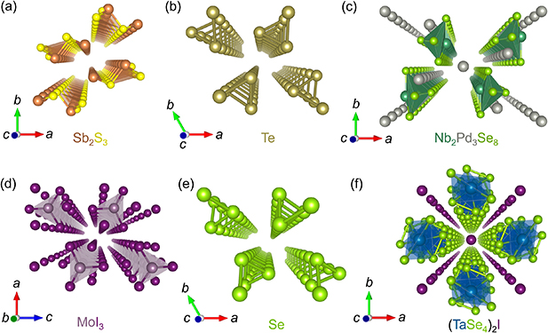
Figure 1. Crystal structures of some typical 1D vdWMs. (a) Sb2S3. (b) Te. (c) Nb2Pd3Se8. (d) MoI3. (e) Se. (f) (TaSe4)2I. The members from the 1D vdWM family typically possess strong covalent bonds in only one direction, while being combined together by weak covalent/ionic bonds or van der Waals interactions in the other two directions.
Download figure:
Standard image High-resolution imageAs a typical attempt in this research domain, in 2021, Yang et al constructed a filterless polarized photodetector based on a 1D Bi2S3 nanowire synthesized via a sulfur-assisted vapor transport method [81]. Figure 2(a) illustrates the crystal structure of Bi2S3 viewed from various perspectives. Apparently, the Bi2S3 crystal is consisted of parallelly aligned (Bi4S6)n atomic ribbons, which extend infinitely along the a-axis. By contrast, the (Bi4S6)n atomic chains are combined together by weak van der Waals bonding along the c-axis. Importantly, the anisotropic crystal structure endows Bi2S3 with anisotropic optical properties. As shown in figure 2(b), density functional theory (DFT) indicates that the light absorbance of Bi2S3 along the a-axis is substantially higher than that along the b-axis. As shown in figure 2(c), the corresponding linear DR of light absorption deviates from unity across the ultraviolet to near-infrared spectral region, laying a solid foundation for polarized photodetection. Specifically, the maximum value of ≈1.8 is realized upon 515 nm light excitation. Taking advantage of the anisotropic light absorbance, the Bi2S3 nanowire photodetectors demonstrate distinct polarization-resolved photoresponse (figures 2(d) and (e)). Specifically, upon 532/808 nm illumination, the linear DR of photocurrent reaches ≈1.41/1.9. In 2022, Shui et al fabricated a polarization-discriminating photodetector toward the optical communication waveband based on a small-bandgap Te microwire [82]. Specifically, upon 1550 nm illumination, the detector demonstrates a responsivity of 170 mA W−1 and a detectivity of 4 × 10⁹ Jones. In addition, a relatively high linear DR of 2.1 has been realized.

Figure 2. (a) Schematic diagrams of the crystal structure of Bi2S3 viewed from various perspectives. (b) Calculated absorbance of Bi2S3 along a-axis (green line) and b-axis (blue line). (c) The corresponding linear dichroic ratio as a function of wavelength of the Bi2S3 crystal deduced from the absorbance. (d)–(e) Polar plots of the polarization angle-resolved photocurrent of the Bi2S3 nanowire device under 808 and 532 nm illuminations, respectively. The solid lines are the fitting results using the sinusoidal function. Reproduced from [81]. CC BY 4.0.
Download figure:
Standard image High-resolution imageIn addition to the individual low-symmetry vdWM nanostructure, heterojunctions based on low-symmetry vdWMs can also be used for polarized photodetection, where the anisotropic photosensitive property of the low-symmetry vdWM component can be well inherited. For example, Wan et al have demonstrated a self-driven photodetector with polarized sensitivity based on a Sb2Se3/GaN 1D/3D heterojunction [83]. Importantly, the device exhibits anisotropic photoresponse with a linear DR of 1.37, which is 1.3 times amplified as compared to a pristine Sb2Se3 photoconductive-type device. Most recently, Luo et al have reported on the polarization-sensitive photoresponse with a linear DR of 2.5 based on a WS2/Te heterojunction photodetector [84]. Of note, drawing upon the dangling-bond-free surface, the construction of van der Waals heterostructures is exempted from the rigorous lattice-matching constrains, a prominent advantage compared to traditional covalent semiconductors such as Si, thus providing multiple potential platforms for the exploration of polarized light sensing.
Thus far, researchers have implemented a series of polarized photodetectors based on various 1D vdWMs, including elemental semiconductors [82, 84–94], binary compounds [81, 83, 95–102], multielemental compounds [63, 103, 104], etc. For clarity, table 1 has summarized the key performance metrics of a wealth of 1D vdWM polarized optoelectronic devices. These advancements have consolidated the enormous application potential of the 1D vdWM family in the optoelectronic identification of the polarization state of incident light.
Table 1. A summary of the performance metrics of polarized photodetectors built of 1D vdWMs.
| Devices | R (A W−1) | EQE (%) | D* (Jones) | Rise/decay time | Dichroic ratio | References |
|---|---|---|---|---|---|---|
| CNT | 28 mV/W | N. A. | 4.69 × 10³ | N. A./32 μs | ≈2 | [94] |
| CNT | 0.1 V/W | N. A. | N. A. | N. A. | ≈2 | [85] |
| CNT | N. A. | N. A. | N. A. | N. A. | 5.06 | [86] |
| CNT | 0.33 V/W | ≈0.8 | 4.33 × 10⁶ | N. A. | ≈16.4 | [87] |
| CNT | 0.2925 | N. A. | N. A. | 42 ms/34 ms | ≈2 | [88] |
| Te | 6650 | N. A. | 1.23 × 10¹² | 31.7 μs/25.5 μs | 5.8 | [89] |
| Te/MoSe2 | 2.106 | 645 | 2.91 × 10¹³ | 25 ms/22 ms | 16.39 | [90] |
| Te/WS2 | 27.8 | N. A. | 9.5 × 10¹² | 19.3 ms/17.6 ms | 2.1 | [91] |
| WS2/Te | 402 | N. A. | 9.28 × 10¹³ | 1.7 ms/3.2 ms | 2.5 | [84] |
| Te | 0.17 | N. A. | 4 × 10⁹ | 33 ms/33 ms | 2.8 | [82] |
| Te | 327 | 26 221 | 6.08 × 10⁷ | 22 ms/23 ms | 2.05 | [93] |
| Bi2S3 | 32 | N. A. | 4.36 × 10¹¹ | 20 ms/10 ms | 1.9 | [81] |
| Bi2S3 | 4.21 | 981.76 | 1.64 × 10¹⁰ | 12.25 ms/12.25 ms | 1.79 | [96] |
| Bi2S3 | 23 760 | 5.55 × 10⁶ | 3.68 × 10¹³ | 1 ms/4.5 ms | 2.4 | [97] |
| Sb2S3 | 0.3434 | N. A. | N. A. | 0.47 ms/0.68 ms | 2.54 | [98] |
| Sb2Se3 | 5.1 | N. A. | 4.4 × 10⁹ | 32 ms/5 ms | 1.63 | [99] |
| Sb2Se3 | 3.61 | 841.24 | 2.36 × 10¹¹ | 30 ms/32 ms | 1.71 | [100] |
| Sb2Se3/GaN | 0.012 | N. A. | 5 × 10¹⁰ | 74 ms/75 ms | 1.37 | [83] |
| Sb2Se3 | 4.39 | 655 | 9.63 × 10¹⁰ | 27 ms/27 ms | 3.95 | [101] |
| SnIISnIVS3 | 290.5 | 8.4 × 10⁴ | 5.2 × 10¹⁰ | <0.4 s/< 0.2 s | 1.3 | [102] |
| BiSeI | 5.88 | 1.3 × 10³ | 2.76 × 10⁸ | 0.11 ms/0.17 ms | 1.77 | [63] |
| Nb2Pd3Se8 | 2.74 × 10⁻³ | N. A. | 4.73 × 10⁶ | 60 ms/55 ms | 1.42 | [103] |
| MoS2/Ta2Pd3Se8 | 2.66 | 970 | 3.5 × 10⁸ | 1.3 μs/2.2 μs | 4.79 | [104] |
a CNT: carbon nanotube. b The output signals of these devices are photovoltage. c N. A.: not applicable.
4. 2D vdWM polarized photodetectors
Generally, 2D vdWMs refer to the ultrathin materials where self-passivated atomic layers are combined by weak van der Waals interactions, whereas the atomic bonding between atoms from the same atomic layer is covalent. In contrast to the widely explored group VIB transition metal dichalcogenides, the fundamental atomic layers of a considerable portion of 2D vdWMs host in-plane anisotropy [105]. The typical members of this family include the group VA elemental semiconductors [106, 107], IVA-VIA compounds [108, 109], group VIII transition metal dichalcogenides [110, 111], multielemental vdWMs [112–114], etc. Accordingly, the low-symmetry lattice structures endow these materials with anisotropic physical properties, such as the anisotropic energy dispersion, laying a solid foundation for the realization polarized devices. As proof of the conception, in 2018, Chen et al unveiled that black arsenic exhibited remarkable anisotropy between the armchair direction and the zigzag direction in terms of its electrical conductance, carrier mobility, and thermal conductivity [107]. Most recently, Liu et al have discovered the anisotropic Raman scattering behaviors in the GaPS4 nanosheets [113]. For clarity, figure 3 presents the crystal structures of some typical anisotropic 2D vdWMs.
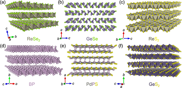
Figure 3. Crystal structures of some typical low-symmetry 2D vdWMs. (a) ReSe2. (b) GeSe. (c) ReS2. (d) Black phosphorus. (e) PdPS. (f) GeS2.
Download figure:
Standard image High-resolution imageOf note, the particular 1D atomic bonding makes 1D vdWMs prone to exist in the form of nanowires [97], nanotubes [101], nanoribbons [115], nanofibrous [116], nanobelts [117], and other ganging morphologies, which is adverse to the construction of device array. Compared to 1D vdWMs, the large-scale preparation of 2D vdWMs is much simpler, laying a solid foundation for the on-chip integration of corresponding functional devices. As an example, in 2021, Wu et al successfully synthesized centimeter-scale uniform few-layer BP through a pulsed-laser deposition technology [118]. Importantly, the corresponding BP device array presents satisfactory device-to-device variation. Most recently, Yang et al have synthesized centimeter-scale Td-MoTe2 film on a flexible mica substrate by molecular beam epitaxy [119]. From this perspective, 2D vdWMs are more suitable for the chip-scale integrated polarization optoelectronics.
As a typical attempt in this research domain, in 2018, Yang et al realized lensless polarization-resolved photodetection by exploiting a GeSe2 nanosheet as the photosensitive channel [120]. The GeSe2 lattice is composed of interconnected GeSe4 tetrahedra (figures 4(a) and (b)). Along the x axis direction, the GeSe4 tetrahedra are connected by sharing the corner atoms. By contrast, along the y axis direction, the Ge2Se8 double tetrahedral are connected by sharing the edges. As a consequence, a lattice structure with inequivalent directions within the basal plane has been formed. Importantly, this brings about anisotropic optical properties. As shown in figure 4(c), the Raman signal is closely dependent on the polarization direction of incident light. Figure 4(d) presents the theoretical absorption spectra along the x-axis and y-axis directions. It is determined that the low symmetry of the lattice structure also gives rise to anisotropic light absorption. As shown in figures 4(e) and (f), the GeSe2 nanosheet photodetector manifests distinct polarization-discriminating photocurrent to 450 nm illumination. Specifically, the linear DR of the device reaches 3.4, which can rival with those of state-of-the-art 1D vdWM polarized photodetectors [84, 97, 98]. Similarly, in 2019, Yang et al fabricated a polarization-resolved UV photodetector by using large-bandgap GeS2 nanosheet as the photosensitive channel [121]. The polarization angle-dependent photocurrent of the device exhibits a distinct two-lobed shape, with a linear DR of 2.1. In 2022, Dai et al demonstrated a long-wave polarized photodetector based on a low-symmetry semimetallic PdSe2 nanosheet [122]. Most notably, upon 4.6/10.5 μm illumination, the linear DR of photovoltage of the device reaches 2.06/1.21.

Figure 4. (a) Side view and (b) top view of the crystal structure of GeSe2. (c) Polarization angle-resolved Raman spectra of a GeSe2 nanosheet. (d) Theoretically calculated light absorption spectra along the x direction (blue line) and the y direction (red line). (e) Schematic diagram of the GeSe2 nanosheet photodetector and the measurement configuration for evaluating polarized photosensitivity. (f) Polar plot of the polarization angle-resolved photocurrent in a normalized way. Reprinted with permission from [120]. Copyright (2018) American Chemical Society.
Download figure:
Standard image High-resolution imageAnalogous to the 1D counterparts, the anisotropic properties of 2D vdWMs can also be well inherited in the corresponding van der Waals heterostructures, providing diversiform platforms toward polarized optoelectronics and thus enabling the implementation of various optoelectronic functional devices. For example, in 2021, Xiong et al successfully constructed a self-powered polarization-sensitive photodetector based on a GeAs/InSe heterojunction [123]. Taking advantages of the low dark current, the device achieves a remarkable on/off ratio of ≈103 under a self-driven mode. In addition, a superior linear DR of ≈18 has been realized upon 635 nm illumination. Most recently, Li et al have demonstrated self-powered polarization-resolved photodetection from visible to near infrared based on a b-As0.4P0.6/MoTe2 heterojunction [124].
Thus far, researchers have prepared numerous polarized photodetectors based on a variety of anisotropic 2D vdWMs, including group VA semiconductors [71, 125–129], non-precious transition metal chalcogenides (MX2 [130–134], MX3 [135–141], MX5 [142]), IIIA-VIA compounds [123, 143, 144], IVA-VA compounds [123, 145–151], IVA-VIA compounds [120, 121, 152–156], precious transition metal chalcogenides [157–164], multielemental vdWMs [72, 73, 165–173], etc. For clarity, table 2 has summarized the key performance metrics of various 2D vdWM polarization-sensitive optoelectronic devices. The extensive advancements have undoubtedly consolidated the immense potential of low-symmetry 2D vdWMs for polarized photodetection. Of note, compared to 1D vdWMs, there have emerged much more low-symmetry 2D vdWMs, greatly enriching the material library toward polarized optoelectronics, which are essential to fully meet the diversified demands of the next generation of polarized optoelectronics.
Table 2. A summary of the performance metrics of polarized photodetectors built of 2D vdWMs with in-plane anisotropy.
| Devices | R (A/W) | EQE (%) | D* (Jones) | Rise/decay time | Dichroic ratio | References |
|---|---|---|---|---|---|---|
| BP | 1.43 | 52 | ≈8.67 × 10⁸ | 1.8 ns/1.68 ns | ≈25 | [125] |
| Black arsenic | 0.44 | 56 | N. A. | N. A. | 2.3 | [126] |
| b-AsP | 0.190 | N. A. | N. A. | N. A. | 14 | [127] |
| BP/ReS2 | 1.8 × 10⁻³ | 0.14 | N. A. | N. A. | 6.44 | [128] |
| HgCdTe/BP | 0.168 | N. A. | 7.93 × 10¹⁰ | 0.15 ms/0.11 ms | 1.45 | [129] |
| b-AsP/WS2/b-AsP | ≈7.2 × 10⁻⁴ | N. A. | >107 | 0.2 ms/0.2 ms | 55 | [71] |
| MoTe2 | 4 × 10⁻⁴ | N. A. | 1.07 × 10⁸ | 31.7 μs/N. A. | 2.72 | [130] |
| WTe2 | N. A. | N. A. | N. A. | N. A. | 1.1 | [131] |
| MoTe2/ReS2 | 0.54 | N. A. | ≈1.32 × 10⁹ | 2.4 μs/3 μs | 1.03 | [132] |
| 2H-MoTe2/1T-MoTe2/SnSe2 | 0.06423 | N. A. | 2.2 × 10¹¹ | 9 ms/14 ms | 2.02 | [133] |
| MoTe2/WS2/MoTe2 | 1.06 | N. A. | 5.64 × 10¹¹ | 48 μs/50 μs | 13 | [134] |
| TiS3 | 2500 | N. A. | N. A. | N. A. | ≈4 | [135] |
| ZrS3 | 5.25 | N. A. | 4.2 × 10⁹ | 117 μs/590 μs | 1.67 | [136] |
| ZrSe3 | 0.0119 | N. A. | 5.24 × 10⁶ | ≈2.8 s/30 s | 1.1 | [137] |
| NbS3 | 0.0247 | N. A. | 5.7 × 10⁸ | 11.6 μs/9.4 μs | 3.95 | [138] |
| TiS3/Si | 0.0348 | N. A. | 1.04 × 10¹⁰ | <0.02 s | ≈4.56 | [139] |
| TiS3/MoS2 | 48 666 | N. A. | 4.96 × 10¹⁴ | 0.4 s/0.4 s | 1.17 | [140] |
| Nb1−x Tix S3 | 2978 | N. A. | 3.23 × 10¹³ | 0.15 s/0.5 s | 1.75 | [141] |
| HfTe5 | 17 V/W | N. A. | 2.7 × 10⁸ | 0.749 ms/N. A. | ≈1.2 | [142] |
| β-InSe | 194 | N. A. | 1.45 × 10¹² | 620 μs/540 μs | 5.66 | [143] |
| γ-InSe | 127 | ≈4 × 10⁴ | 2.73 × 10¹¹ | N. A. | 2.07 | [144] |
| GeAs/InSe | 1.2 | N. A. | 2 × 10¹¹ | 25 ms/25 ms | 18 | [123] |
| SiP | 2.02 | N. A. | 1.88 × 10¹⁰ | N. A. | 1.4 | [145] |
| SiP2 | 0.31 | 105 | ≈1.28 × 10¹² | 3 ms/3.5 ms | 1.6 | [146] |
| SiAs | 0.016 | 1.2 × 10³ | 1 × 10¹⁰ | <1 s/< 1 s | 5.3 | [147] |
| GeAs | N. A. | N. A. | N. A. | 52 ms/55 ms | 4.4 | [148] |
| GeAs2 | N. A. | N. A. | N. A. | N. A. | ≈2 | [149] |
| GeAs/WS2 | 0.509 | 99.8 | 1.08 × 10¹² | 1.5 ms/1.3 ms | 4.5 | [150] |
| GeS | N. A. | N. A. | N. A. | N. A. | 1.45 | [152] |
| GeS2 | N. A. | N. A. | N. A. | N. A. | 2.1 | [121] |
| GeSe | 1.6 × 10⁵ | 3.9 × 10⁷ | 2.9 × 10¹³ | 0.28 s/0.51 s | 1.3 | [153] |
| GeSe2 | N. A. | N. A. | N. A. | N. A. | 3.4 | [120] |
| SnS | 310.5 | 8.56 × 10⁴ | N. A. | 0.45 s/3.14 s | ≈1.17 | [154] |
| SnSe | 9.27 | 2077 | 4.08 × 10¹⁰ | 0.28 μs/0.286 μs | 2.31 | [155] |
| GeSe/MoS2 | 0.105 | 24.2 | 1.46 × 10¹⁰ | 0.11 s/0.75 s | 2.95 | [156] |
| ReS2 | ≈3.59 × 10³ | N. A. | N. A. | N. A. | ≈4.15 | [157] |
| PdSe2 | 1.3 × 10⁻³ | N. A | 2.55 × 10⁷ | 4 μs/14 μs | 1.3 | [158] |
| PdSe2/FA1−x Csx PbI3 | 0.313 | ≈52.2 | 2.72 × 10¹³ | 3.5 μs/4 μs | 6.04 | [159] |
| WS2/ReS2 | 1.85 × 10⁻³ | N. A. | N. A. | 1.3 ms/0.85 ms | ≈1.76 | [160] |
| ReS2/ReSe2 | 126.56 | N. A. | 3.16 × 10¹¹ | 6 μs/8.9 μs | ≈2 | [161] |
| WSe2/ReSe2 | 0.57 | N. A. | ≈109 | 2 μs/2.5 μs | ≈2 | [162] |
| GaSe/ReS2 | 0.17 | 10 | 5 × 10⁹ | 0.261 s/0.274 s | 3.03 | [163] |
| GaAs/ReS2 | 6.86 | 1639 | 1.2 × 10⁹ | 20 s/30 s | 1.71 | [164] |
| TaIrTe4 | 3.4 × 10⁻⁴ | N. A. | 2.7 × 10⁷ | 25.73 μs/N. A. | 1.88 | [165] |
| NbOI2 | ≈5.92 | N. A. | N. A. | 3 s/4 s | 1.7 | [72] |
| Ta2NiSe5 | 44 | N. A. | 1.2 × 10¹² | 98 ms/82 ms | 3.24 | [166] |
| CrPS4 | 1.37 × 10⁻⁷ | N. A. | 5.82 × 10⁷ | <2 s/ < 2 s | 1.33 | [167] |
| PdPS | 1.18 × 10³ | N. A. | 4.4 × 10¹¹ | 1.4 ms/1.2 ms | 3.7 | [168] |
| ZrGeTe4 | 0.62565 | 145.9 | 1.73 × 10⁷ | 4 ms/8 ms | 2.04 | [169] |
| MnBi2Te4 | 0.76 | N. A. | N. A. | 1 μs/1.3 μs | >30 | [73] |
| Ta2NiS5 | 2.5 × 10⁻³ | N. A. | N. A. | 31.1 μs/N. A. | 1.31 | [170] |
| NbIrTe4 | 9.48 | N. A. | N. A. | 0.46 μs/7.2 μs | 14.1 | [171] |
| TaIrTe4/WSe2 | 9.1 | 2776 | 3.89 × 10¹² | 22.5 ms/25.1 ms | 1.75 | [172] |
| WSe2/TaIrTe4/MoS2 | 1.48 | N. A. | 2.39 × 10¹¹ | 12.44 ms/16.52 ms | 9.1 | [173] |
a b-AsP: Black arsenic phosphorus. b N. A.: not applicable. c The output signals of these devices are photovoltage.
5. Polarizing strategies
Despite the significant research progress, low-dimensional vdWM polarized photodetectors have still been confronted with the following pivotal challenges. Firstly, some of the most widely explored low-dimensional vdWMs (such as graphene, MoS2, WS2, MoSe2, WSe2, etc) harbor relatively high in-plane symmetry in their crystal structures. In this consideration, the corresponding optoelectronic devices can only detect the power intensity/wavelength of incident light, whereas the identification of the polarization characteristics is infeasible for the pristine high-symmetry material and their heterostructures [174–176]. On the other hand, although the intrinsic low symmetry of the crystal structures can induce anisotropic photoresponse, the linear DRs of a plethora of low-dimensional vdWM polarization-discriminating photodetectors have still been relatively low [146, 167, 177, 178], which is quite adverse to the implementation of reliable detection of the polarization direction. This deficiency has posed a severe challenge to the practical application of vdWM polarized photodetectors. Secondly, due to the relatively weak light absorption of low-dimensional materials and the relatively short lifetime of their photogenerated charge carriers induced by the strong spacial confinement, the photosensitivity of the pristine low-dimensional vdWM photodetectors is relatively low. In response to the above-mentioned critical scientific challenges, researchers have developed a series of exceptional strategies to enhance the optoelectronic dichroism of low-dimensional vdWMs and improve their photoelectric properties.
5.1. Quantum tailoring
In addition to the intrinsic anisotropy enabled by the low-symmetry microscopic crystal structures (e.g. Bi2S3, Sb2S3), the extrinsic geometric size of 1D vdWMs is also one of the key parameters affecting their polarization characteristics. As an example, in 2019, Ghoshal et al found that the polarization ratio of the PL emission attenuates with increasing sample width [179]. In this regard, it can be reasonably deduced that the polarization-discriminating photoresponse of 1D vdWM photodetectors will be closely related with the geometric size.
To this end, most recently, Yi et al have systematically studied the influence of the degree of quantum confinement on the polarization-dependent photosensitivity of 1D vdWM photodetectors by taking Bi2S3 nanowires as the research subjects [97]. As shown in figures 5(a)–(f), as the height/width of the Bi2S3 nanowire decreases, the linear DR of photocurrent of the Bi2S3 photodetector monotonically increases. That is, there exists a positive correlation between the optoelectronic dichroism and the degree of spacial quantum confinement of the semiconductor nanowire. Specifically, an optimal linear DR of ≈2.4 has been demonstrated upon 405 nm illumination. To garner an in-depth insight, systematic finite-difference time domain (FDTD) simulations have been performed. As shown in figures 5(g)–(i), the ratio of the absorption cross section (ACS)/scattering cross section (SCS) of a Bi2S3 nanowire upon parallel polarization light excitation to that upon perpendicular polarization light excitation increases with the decrease of the height/width of the nanowire (i.e. increasing quantum confinement). As a consequence, the linear DR of the corresponding Bi2S3 photodetectors will increase as the width/height of the nanowire attenuates.
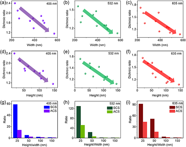
Figure 5. (a)–(c) Linear dichroic ratio as a function of the channel width upon 405, 532, and 635 nm illuminations. (d)–(f) Linear dichroic ratio as a function of the channel height upon 405, 532, and 635 nm illuminations. (g)–(i) Anisotropic ratios of ACS (purple columns) and SCS (blue columns) as a function of the width/height of the Bi2S3 nanowire upon 405 nm, 532 nm, and 635 nm excitations. Reproduced from [97] with permission from the Royal Society of Chemistry.
Download figure:
Standard image High-resolution imageIn principle, the azimuth-dependent photoresponse of the Bi2S3 nanowire photodetectors is mainly attributed to the anisotropic dielectric contrast [180]. The dielectric constant of a semiconductor (e.g. ≈15 for Bi2S3 [181]) is generally much higher than that of air (≈1). Therefore, as for a 1D semiconductor, the dielectric contrast along the direction perpendicular to the axial direction is much more pronounced than that along the direction parallel to the axial direction. This thus results in anisotropic light–matter interactions, thereby leading to polarization-sensitive photoresponse. From the above fundamental mechanism, it can be rationally determined that the quantum tailoring strategy can be theoretically applicable to various 1D vdWMs, providing a flexible and universal pathway for further optimizing their photoelectric dichroism in the future.
Currently, although researchers have successfully prepared a series of 1D vdWM nanowires, such as Te [93], Se [182], Sb2S3 [98], Nb2Pd3Se8 [103], SnIISnIVS3 [102], and etc, the sizes of the products are highly stochastic. There has still been a lack of a reliable synthesis technique that can finely regulate the diameter of the vdWM nanowires. Most recently, Ma et al have unveiled that the anisotropic growth of the Sb2Se3 crystal can be flexibly tuned by simply modulating the growth temperature [99]. Specifically, as the growth temperature increases from 700 °C to 850 °C, the product's width decreases monotonously from ≈498 to ≈172 nm. In another work, Yi et al have discovered that the use of additional sulfur powder precursor can substantially augment the anisotropic ratio of the Bi2S3 nanowires grown by atmospheric pressure chemical vapor deposition [97]. These studies have provided useful insights for the regulation of the dimension of 1D vdWMs. In the future, more research efforts on the customized acquirement of diameter are anticipated for the delicate quantum tailoring of 1D vdWM polarization-discriminating photodetectors, and the underlying growth mechanisms remain to be unveiled from the dynamics and thermodynamics perspectives.
5.2. Construction of core–shell structures
Another potential symmetry-reduction strategy is to construct a core–shell heterostructure. For example, previous studies have suggested that the anisotropy of photoresponse of the core–shell GaAs/AlGaAs photodetectors is substantially higher than that of pristine GaAs photodetectors under similar conditions [183, 184]. Nevertheless, thus far, the effect of core–shell structure on the dichroism of low-dimensional vdWM photodetectors has still been rarely explored.
To this end, in 2020, Xiao et al developed the SbI3/Sb2O3 core–shell van der Waals heterojunctions for filterless polarization-sensitive photodetectors (figure 6(a)) [185]. In this study, the core–shell heterostructures are prepared by a simple two-step method. Firstly, single crystalline gangly SbI3 strips are synthesized by a chemical vapor transport method, followed by the downscaling treatment via typical micromechanical exfoliation. Then, an outer oxidation layer (Sb2O3) surrounding the SbI3 nanostrip is prepared via surface's autoxidation in the air environment. As shown in figures 6(b) and (c), DFT calculations predict that the anisotropy of light absorption of the SbI3/Sb2O3 core–shell van der Waals heterojunction has been significantly improved compared to pristine SbI3 and Sb2O3. Specifically, the maximum linear DR of light absorption of SbI3/Sb2O3 reaches ≈3.74. By contrast, the linear DR of light absorption of SbI3 is only ≈1.72 at the same wavelength, and the Sb2O3 exhibits isotropic light absorption due to the intrinsic high symmetry of the Fd-3m space group. As shown in figures 6(d) and (e), the core–shell SbI3/Sb2O3 photodetector has exhibited distinct polarization-resolved photosensitivity under 450 and 532 nm illuminations. Specifically, upon 450 nm illumination, the highest linear DR of photocurrent reaches ≈3.14, which is much higher than those of the pristine SbI3 (≈1.16) and Sb2O3 (≈1) photodetectors. On the whole, this study has depicted a flexible scheme to promote the anisotropy of low-dimensional vdWM photodetectors.
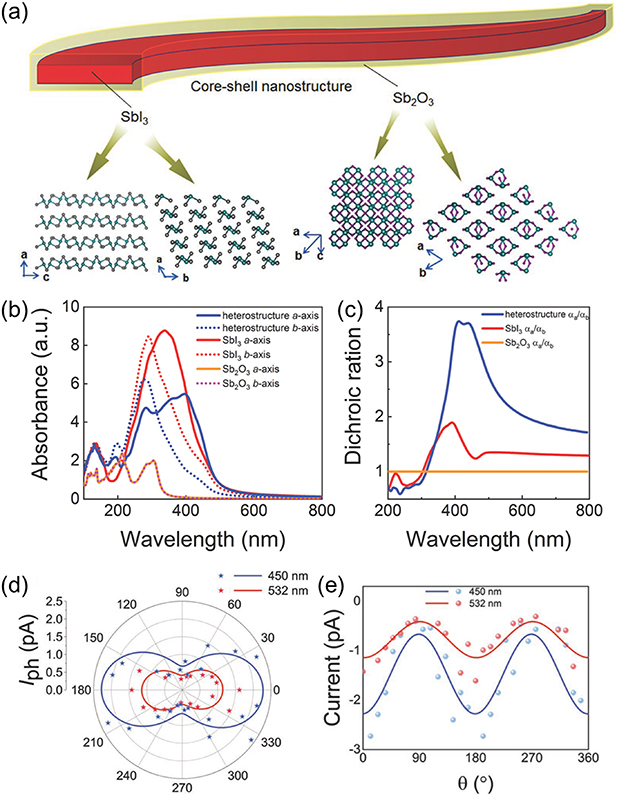
Figure 6. (a) Schematic illustration of the SbI3/Sb2O3 core–shell heterojunction. The bottom images present the crystal structures of SbI3 (left) and Sb2O3 (right). (b) The theoretical absorbance curves along a-axis (solid lines) and b-axis (dashed lines) of the SbI3/Sb2O3 heterostructure, SbI3, and Sb2O3, respectively. (c) The corresponding linear dichroic ratio as a function of wavelength of the SbI3/Sb2O3 core–shell heterostructures (blue line), SbI3 (red line), and Sb2O3 (orange line). (d) Polar plots of the polarization angle dependent photocurrent upon 450 nm (blue stars) and 532 nm (red stars) illuminations. The blue and red lines are fitting curves by the function of Iph = Ipx cos2(δ + ϕ) + Ipysin2(δ + ϕ). (e) Polarization angle dependent photocurrent upon 450 and 532 nm illuminations in an orthogonal coordinate. [185] John Wiley & Sons. © 2020 WILEY‐VCH Verlag GmbH & Co. KGaA, Weinheim.
Download figure:
Standard image High-resolution imageThus far, a variety of 1D vdWMs based core–shell heterostructures, including Sb2Se3/Sb2S3 [186], Sb2S3/CdS [187], and MoS2/Sb2Se3 [188], have been successfully prepared. Due to the reduction of symmetry, these core–shell heterostructures will hold enormous potential for application in polarization-discriminating photodetection. Of note, in addition to reducing symmetry, these core–shell heterostructures can also be conducive to increasing the separation efficiency of photogenerated carriers through the formation of interfacial built-in electric field, thereby suppressing the recombination of non-equilibrium photocarriers [189, 190]. In addition, with reasonable energy band design, the core and shell materials with complementary optical properties can leverage synergistic effects in the spectral photoresponse, thereby enabling the implementation of high-performance and broad-spectrum polarized light sensing.
5.3. Rolling engineering
Although a plethora of polarization-resolved low-dimensional vdWM photodetectors have been implemented based on low-symmetry photosensitive materials with strong in-plane anisotropy, these materials suffer from severe deficiencies in the current stage. For example, the air-stability the group-VA semiconductors (e.g. BP, black arsenic) is quite poor, while the cost of the group VIII transition metal dichalcogenides (e.g. PdSe2) is much too high. Furthermore, the synthesis of these low-symmetry materials, especially the large-area preparation, is still comparatively challenging. This makes further breakthroughs in the performance of the corresponding functional devices and their on-chip integration extremely challenging. By contrast, the synthesis of high-symmetry vdWMs (such as graphene, h-BN, MoS2, and WS2) has been relatively mature [191–194], because their in-plane growth is largely isotropic, benefiting from the high-symmetry internal crystal structures. In this consideration, the development of artificial polarization-discriminating photodetectors based on low-dimensional vdWMs with high symmetry has become particularly impending. To this end, researchers have developed a series of strategies to introduce polarization-resolved photosensitive properties in highly symmetric vdWMs.
In 2020, Deng et al conceived and developed a rolled-up strategy for monolayer MoS2 photodetectors, simultaneously inducing polarization-resolved photoresponse and promoting the photosensitivity (figure 7(a)) [195]. In this study, a self–rolled-up technique has been utilized to transform the 2D MoS2 nanosheets into 3D MoS2 microtubes. Firstly, a highly strained silicon nitride (SiNx ) nanofilm is deposited onto the top of an Al sacrificial layer, followed by the deposition of a Cr/Au gate electrode and a SiO2 dielectric layer. Secondly, a single-layer MoS2 nanosheet is transferred atop, followed by the patterning of source and drain electrodes. Finally, the 2D MoS2 phototransistor is rolled into a 3D tubular structure by releasing the strain of the SiNx nanofilm, which is realized by etching away the Al sacrificial layer. Impressively, the tubular geometric structure endows the 3D device with fascinating polarization-dependent optoelectronic properties. As shown in figures 7(b) and (c), it is evident that the photocurrent is highly dependent on the polarization direction of the linearly polarized incident light under various bias conditions, exhibiting a periodical evolution. Specifically, the linear DR reaches ≈1.64, which is comparable to those of some of the state-of-the-art low-symmetry vdWM photodetectors [63, 136, 196, 197]. The unique polarization-discriminating photosensitivity is attributed to that the self-rolled 3D MoS2 phototransistor can function as a low-symmetry optical resonator, where the optical resonant modes are highly polarized. In addition to inducing anisotropic photoresponse, this 3D tubular structure can also enhance the photosensitivity. As shown in figure 7(d), the responsivity values of the tubular MoS2 devices have been greatly augmented compared to the pristine planar counterparts. In addition, the responsivity also increases with increasing rolling cycles.

Figure 7. (a) Schematic diagram of a 3D MoS2 phototransistor for polarization-discriminating photodetection. The polarization angle (θ) is defined as the angle between the polarization direction of linearly polarized incident light and the axial direction of the MoS2 roll. (b) Normalized polarization angle dependent photocurrent of a 3D MoS2 phototransistor under different source–drain voltages, where Iph,0 represents the photocurrent measured under the polarization angle of 0°. (c) The corresponding polar plots of the data in (b). (d) Responsivity as a function of light power density of 2D MoS2 photodetector (black line) and 3D MoS2 photodetectors with one winding (blue line) and two windings (red line). (e) The spacial distribution of the electric field magnitude in vicinity of a 3D MoS2 roll with one rolled-up winding under 395 nm illumination. (f) The average normalized electric field magnitude (E3D/E0) at the surface of 3D MoS2 rolls with various rolled-up windings. Reproduced from [195]. CC BY 4.0.
Download figure:
Standard image High-resolution imageAs shown in figure 7(e), FDTD simulations have consolidated that the enhancement of the photosensitivity is originated from the enhancement of the optical field (i.e. the electromagnetic field). The incident light resonates in vicinity of the interior and exterior surfaces of the 3D MoS2 microtube in an evanescent mode. That is, the electric field magnitude augments exponentially with decreasing distance away from the surfaces because of the ingenious microcavity provided by the tubular geometry. Specifically, the average electric field amplification magnitude (E3D/E0) at the interior surface approaches ≈282, enabling much more efficient light harvesting. In addition, the average electric field amplification magnitude augments with increasing rolled-up winding number (figure 7(f)). Moreover, the ACS enlarges with increasing rolling cycles. Accordingly, the photosensitivity augments with increasing rolled-up winding number.
On the whole, rolling engineering enables the transformation of planar materials from 2D to 3D and this approach thus can enhance the light absorption while artificially imparting polarization-resolved photodetection capability to high-symmetry materials via low extrinsic geometric symmetry of device. This paradigm presents a universal avenue to induce polarized photosensitivity whilst addressing the well-known high transmission loss deficiency of low-dimensional vdWM optoelectronic devices caused by their nanoscale active layers.
Thus far, in addition to MoS2, the rolling strategy has been widely applied to a variety of high-symmetry vdWMs, including graphene [198], reduced graphene oxide [199], h-BN [200], MoSe2 [201], WS2 [202], and even van der Waals heterostructures [203–205]. Similarly, these 3D tubular structures hold indisputable prospects in the polarization-dependent photodetection, and their polarization photosensitivity is still in need of further investigation. Nevertheless, it is to be emphasized that rolling 2D materials is rather time-consuming and cumbersome, and the rolling processing may inevitably induce structural defects. These drawbacks markedly plague the practical application of this technique. Most recently, An et al have demonstrated the direct growth of high-quality WS2 and WSe2 nanotubes by exploiting catalytic chemical vapor deposition with Au nanoparticles [206]. Basically, the Au nanoparticles provide unique accommodation sites for the nucleation of WS2 or WSe2 shells on the surfaces and seed the growth of nanotubes. This growth strategy has markedly facilitated the preparation of transition metal dichalcogenides nanotubes, providing a flexible avenue for the production of nanotube-based polarization-sensitive photodetectors. On the other hand, besides the rolling cycles, the diameter of the 3D microtube, which is closely associated with the geometric anisotropic ratio, is probably another underlying parameter dominating the device properties. Most recently, Yi et al have unveiled that the linear DR of Bi2S3 nanowire photodetectors is negatively correlated with the height/width of the photosensitive channel [97]. Therefore, it can be rationally expected that the rolling diameter will manifest a significant impact on the polarization photoelectric characteristics of the corresponding devices, and further exploration is of urgent demand in the upcoming future.
5.4. Ferroelectric regulation
Another potential strategy to induce/enhance the anisotropy of low-dimensional vdWM electronic devices is the exertion of ferroelectric polarization. As an example, in 2019, Wang et al revealed that the anisotropy of the electrical transport property of 2D ReS2 nanosheets can be markedly modulated by simply tuning the polarization state of the adjacent ferroelectric layer [207].
To exert the potency of ferroelectric regulation on the anisotropic photoresponse of low-dimensional vdWM photodetectors, in 2022, Wu et al systematically studied the influence of ferroelectric polarization on the azimuth-dependent photosensitivity of 2D BP [208]. As shown in figure 8(a), Poly(vinylidene fluoride-trifluoroethylene) (P(VDF-TrFE)) is employed as the ferroelectric layer, which is covered on the top of a BP channel by a spin-coating method. As shown in figure 8(b), compared with the counterpart without directional ferroelectric polarization, the linear DR of a BP phototransistor with ferroelectric polarization has been distinctly improved. Specifically, upon 520 nm light illumination, the linear DR has been increased from ≈1.36 to ≈1.62. Upon 1450 nm light illumination, the linear DR has been increased from ≈1.73 to ≈2.42. On the other hand, homostructures formed by ferroelectric polarization can also improve the dichroism of photoresponse. As shown in figure 8(c), a BP p–n junction can be implemented by patterning ferroelectric layers with opposite polarization directions on the two sides of the BP channel. As shown in figure 8(d), the photoresponse of the BP p–n junction exhibits pronounced anisotropy. Specifically, upon 520 nm light illumination, the linear DR of the device reaches ≈3.9. Upon 1450 nm light illumination, the linear DR of the device reaches ≈288, which is at the leading level among the reported BP based polarization-sensitive photodetectors (figure 8(e)). Since the enhancement of polarized photosensitivity is predominantly emanated from the ferroelectric polarization state of the adjoining ferroelectric layer, the ferroelectric polarization engineering strategy in this study can theoretically be adopted to other low-dimensional vdWMs. Overall, this study has depicted a potentially universal landscape for further optimizing the dichroism of low-dimensional vdWMs based polarized photodetectors.
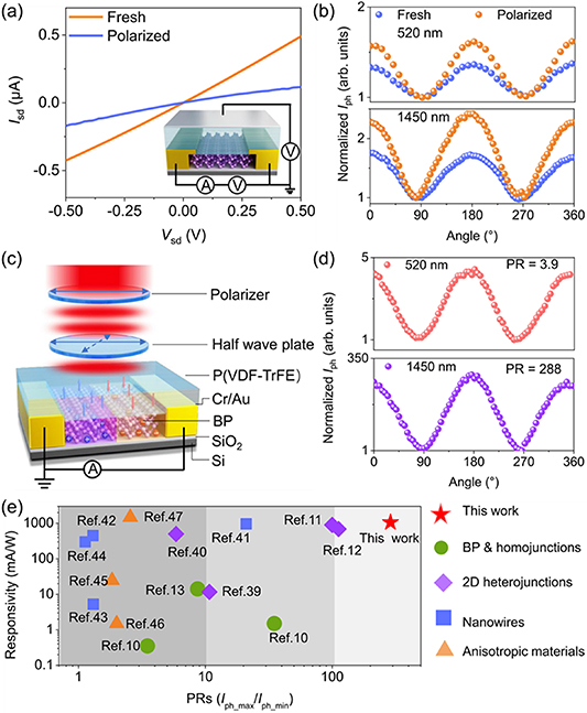
Figure 8. (a) Output characteristics of the pristine (orange line) and polarized (blue line) black phosphorus phototransistors. The inset presents the device structure. (b) Normalized photocurrent of the device at the fresh (blue dots) and polarized (orange dots) states as a function of the polarization angle upon 520 (top panel) and 1450 (bottom panel) nm illuminations, respectively. (c) Schematic of black phosphorus in-plane p–n homojunction defined by ferroelectric domains. (d) Normalized photocurrent of the black phosphorus in-plane p–n homojunction as a function of the polarization angle upon 520 and 1450 nm illuminations, respectively. Polarization ratio (PR) is defined as the ratio of the maximum photocurrent to the minimum photocurrent. (e) Responsivity and PR of black phosphorus in-plane p–n homojunction defined by ferroelectric domains compared with black phosphorus, black phosphorus homojunctions defined by other methods, 2D heterojunctions, nanowires, and other anisotropic materials, showing that this work is at the leading level among most of the previously reported polarization photodetectors. Reproduced from [208]. CC BY 4.0.
Download figure:
Standard image High-resolution imageIt is worth noting that a plethora of low-dimensional vdWMs, including AgBiP2Se6 [209], CuInP2S6 [210], Bi2TeO5 [211], α-In2Se3 [212, 213], β*-In2Se3 [214], GeS [215], GeSe [216], GaSe [217], SnSe [218], SnS [41], Bi2O2Se [219], Sn2P2S6 [220], Co2NF2 [221], Bi1.8Sm0.2O3 [222], etc, have thus far proven to host intrinsic ferroelectricity. Furthermore, in addition to coupling with the extrinsic ferroelectric layer, previous studies have consolidated that the ferroelectricity of the photosensitive materials themselves can also bring about anisotropic photoresponse [223–226]. As an example, Li et al have implemented a polarized photodetector with a linear DR of ≈2 based on a novel 2D hybrid perovskite ferroelectric ([CH3(CH2)3NH3]2(CH3NH3)Pb2Br7) [223]. Most recently, Liu et al have reported on a giant DR of ≈25 in a ferroelectric (HA)2(EA)2Pb3Br10 photodetector [227]. Of note, the exemption of the extrinsic ferroelectric layer in this case can effectively simplify the preparation of devices and increase their integration. Accordingly, the correlation between the ferroelectric polarization state and the azimuth-resolved photosensitive property of low-dimensional ferroelectric vdWMs represents a highly worthy research topic, and more efforts are needed for this research domain in the upcoming future.
5.5. Strain engineering
Anisotropic low-dimensional vdWMs have exhibited remarkable polarized properties in optics, electricity, and optoelectronics, making them promising for a wide range of applications and attracting for extensive research enthusiasm. However, low-dimensional vdWMs with intrinsic anisotropy arising from the low-symmetry crystal structure are currently challenging to achieve mature and controllable large-area preparation, since their growth commonly tends to be anisotropic [97, 228, 229]. Considering the wafer-level controllable preparation of the widely explored high-symmetry low-dimensional vdWMs (e.g. graphene [230], MoS2 [231, 232], etc), one potential approach to address the predicament is to artificially endow the crystal structure with anisotropy. Strain engineering has proven as a very effective strategy to introduce anisotropy into isotropic low-dimensional vdWMs. For example, in 2017, Martella et al found that the MoS2 layer grown on a rippled SiO2/Si substrate, which can induce localized strain, exhibited strongly anisotropic phonon modes [233]. In another study, He et al unveiled that the second-harmonic generation pattern of WS2 evolved from a classic six-fold pattern to a distorted six-fold pattern under the uniaxial strain [234]. On the basis of the foregoing results, strain engineering is an attractive approach to induce and manipulate anisotropy for polarized optoelectronic devices.
In 2019, Tong et al for the first time reported the successful control of in-plane crystal symmetry by artificially inducing uniaxial tensile strain to a monolayer MoS2 photodetector, which brought about distinct polarization-resolved photosensitivity [235]. In this study, the monolayer MoS2 is transferred onto a flexible polydimethylsiloxane (PDMS) substrate. The uniaxial tensile strain is applied by stretching the PDMS substrate, where a portion of strain will be delivered to the atop MoS2 layer. As shown in figures 9(a) and (b), the introduction of uniaxial tensile strain reduces the overall in-plane symmetry of the crystal structure of MoS2, with a consequent modification of the Brillouin zone. As shown in figure 9(c), compared to the pristine MoS2 device exhibiting isotropic photoresponse [237], the uniaxial tensile strain endows the device with polarization angle-dependent photocurrent. Furthermore, the linear DR can be tuned by flexibly adjusting the extrinsic strain. Specifically, under 4.5% tensile strain, the linear DR can reach up to ≈2, which is comparable to those of low-dimensional vdWMs with intrinsic anisotropy arising from the low-symmetry crystal structures [121, 126, 238].

Figure 9. (a) Comparison of the in-plane crystal structures of pristine MoS2 and MoS2 upon external tensile strain. (b) The Brillouin cells of pristine MoS2 and MoS2 upon external tensile strain. (c) Polarization angle-resolved photocurrent of a MoS2 photodetector under various strain values. Reprinted from [235], © 2019 Elsevier Ltd. All rights reserved. (d) Schematic diagram of the WSe2/CrOCl photodetector. (e) Photoswitching curves of the WSe2/CrOCl device under 532 nm illuminations with different polarization angles. (f) Polar plot of the photocurrent as function of polarization angle under 532 nm illumination. [236] John Wiley & Sons.© 2022 Wiley‐VCH GmbH.
Download figure:
Standard image High-resolution imageIn addition to stretching, the interlayer coupling-induced axial strain can also impart anisotropy to high-symmetry low-dimensional vdWMs. Most recently, Wei et al have developed a WSe2/CrOCl heterojunction for inducing distinct linear dichroism of photoresponse (figure 9(d)) [236]. As shown in figures 9(e) and (f), the photocurrent of the WSe2 photodetector built on a CrOCl substrate evolves periodically with the polarization angle with a period of 180°. Specifically, when the polarization direction of incident light is parallel to the zigzag direction of CrOCl, the photocurrent reaches its lowest value. By contrast, when the polarization direction of incident light is perpendicular to the zigzag direction of CrOCl, the photocurrent reaches its highest value. Upon 532 nm illumination, the linear DR reaches ≈1.27. Similarly, in another research work, Zheng et al have achieved polarization-resolved photoelectric sensing with a linear DR of ≈1.25 by coupling a MoS2 photodetector with a CrOCl substrate [239], consolidating the excellent general applicability of this strategy. Although the effect of strain still needs further improvement, these studies have exemplified a distinctive approach for artificially regulating the dichroism of low-dimensional vdWM optoelectronic devices.
Thus far, researchers have developed a series of strain modulation strategies for low-dimensional vdWMs, such as polymer encapsulation [240], coupling with uneven substrates [35, 241–244], wrinkling treatment [245], bending [246, 247], strained epitaxy [248], thermal expansion [249], etc. In the future research, these strategies can theoretically be adopted to modulate the polarized photosensitivity of low-dimensional vdWM photodetectors toward more pronounced anisotropy. Of note, in addition to the individual vdWM, strain can also induce polarity into van der Waals heterostructures. For example, in 2020, Bai et al demonstrated polarization-sensitive PL emission in a WSe2/MoSe2 heterostructure by applying differential and uniaxial tensile strain [250]. This is because that strain can transform the moiré pattern into a hierarchy consisted of numerous parallel elongated ovals to form a secondary structure of pseudo-1D stripes, which can further merge into 1D stripes for sufficiently small twist angle. In this consideration, strain engineering can also be exploited to tailor the polarized photosensitivity of van der Waals heterojunction photodetectors. However, a potential tricky challenge of the strain engineering strategy is that the strained state is commonly a metastable state. In this regard, an approach to stabilize the strain may be essential in the future.
5.6. Integration of low-symmetry optical antennas
From a fundamental perspective, the polarized photosensitivity of low-symmetry vdWM photodetectors comes from the anisotropic light absorption, which is derived from the anisotropic energy dispersion of the band structure. On the other hand, nanoantennas, the artificial subwavelength periodic architectures, offer immense flexibility in tailoring the optical properties, and low-symmetry noble metal nanostructures have been known to exhibit anisotropic optical properties [251]. Therefore, an alternative and effective approach to enhance the polarized photosensitivity of low-dimensional vdWM photodetectors is to integrate low-symmetry optical antennas. By manipulating the structures of optical antennas, it is feasible to actively modify the light absorption property of low-dimensional vdWM photodetectors, thereby directing their photoresponse towards specific orientation. This can be accomplished through the utilization of plasmonic resonance antennas.
As a proof, in 2018, Venuthurumilli et al demonstrated an improved polarization selectivity in 2D BP with a high linear DR of ≈8.7 at the near-infrared wavelength of 1550 nm by employing bowtie aperture plasmonic structures (figure 10(a)) [252]. The bowtie apertures are fabricated onto the BP flakes using standard electron beam lithography, metallization, and lift-off processes. As shown in figure 10(b), the BP photodetector integrated with bowtie apertures exhibits markedly improved linear DR of ≈5.8–1550 nm illumination (1.05 mW) as compared to a pristine BP counterpart device (≈4.0). At a lower laser power of 470 μW, a higher linear DR of ≈8.7 is achieved. As shown in figure 10(c), FDTD simulations suggest that the light absorption upon armchair polarization excitation is substantially stronger than that upon zigzag polarization excitation. This is because that the bowtie apertures only substantially enhance the light absorption in the armchair direction, whereas there is little enhancement in the zigzag direction (figure 10(d)). As a consequence, an improved polarization photosensitivity is realized. On the whole, nanoantenna-mediated low-dimensional vdWM photodetectors can enable the augmentation of the degree of anisotropy of polarization-discriminating photosensitivity by tailoring the nanoantenna near-field distribution via delicate geometry design.

Figure 10. (a) Optical image and SEM images of a black phosphorus photodetector integrating a bowtie aperture array. (b) Polarization ratio as a function of light power of black phosphorus photodetectors with and without bowtie apertures upon 633 and 1550 nm illuminations. (c) Computed absorption as a function of wavelength along the armchair and zigzag directions of black phosphorus integrated with bowtie apertures. (d) Top view of the electric field distribution in vicinity of a bowtie aperture under illuminations along the armchair (left) and zigzag (right) directions, respectively. Reprinted with permission from [252]. Copyright (2018) American Chemical Society. (e) Schematic depiction of a graphene phototransistor with integrated plasmonic cavity. (f) Polarization angle dependent photoresponse in a polar plot of the graphene phototransistor integrated with plasmonic cavity under 1550 nm illumination. Reprinted from [253], with the permission of AIP Publishing. (g) 3D schematic diagram of a metasurface-mediated graphene photodetector. (h) Polarization angle dependent photovoltage of graphene photodetectors with metasurfaces of various geometries. Reproduced from [257]. CC BY 4.0. (i) Schematic illustration depicting the graphene photodetector integrated with monolithic metamaterial. (j) Polarization angle dependent photovoltage upon illuminations with frequencies of 2.52 and 3.11 THz. Reprinted with permission from [259]. Copyright (2022) American Chemical Society.
Download figure:
Standard image High-resolution imageBy integrating low-symmetry optical antennas, polarization-resolved photoresponse can also be achieved in high-symmetry low-dimensional vdWMs, even that these materials are in the absence of inherent anisotropy. For example, graphene exhibits a wealth of excellent properties, such as broad effective optical window, high sensitivity, fast response, and chemical stability, making it amenable to the fabrication of high-performance broadband photodetectors. Nevertheless, graphene is considered to be polarization insensitive on account of its high-symmetry hexagonal lattice structure. To this end, in 2019, Zhang et al developed a graphene phototransistor integrated with an anisotropic plasmonic cavity for polarization detection (figure 10(e)) [253]. This structure facilitates the surface plasmonic oscillations between the metal stripes and the dielectric spacer, resulting in a pronounced enhancement of the electromagnetic field when resonance is achieved. This electric field enhancement leads to a high absorption of the incident light with polarization direction perpendicular to the direction of the metal stripes. Conversely, the majority of the light with polarization direction parallel to the direction of the metal stripes is reflected, resulting in low absorption. As a consequence, anisotropic photoresponse with a remarkable linear DR of ≈30 is realized (figure 10(f)). Following this success, in 2020, Chen et al developed a MoS2-based polarized photodetector by integrating elliptical Au nanostructure antennas atop [254]. Noteworthily, the ratio of the maximum photocurrent to the minimum photocurrent of the hybrid device reaches 1.45. Moreover, profiting from the strong resonant coupling absorption enhancement, the responsivity of the MoS2/Au photodetector is approximately twice that of the pristine MoS2 device. In 2021, Wei et al demonstrated configurable polarity transition by tuning the orientation of nanoantennas in tapered nanoantenna modified graphene photodetectors [255]. Importantly, the DR can approach infinity at the polarity-transition point, allowing the subtle measurement of polarization-angle perturbation down to 0.02° Hz−1/2 in the mid-infrared spectral range. Most recently, Fan et al have constructed broadband polarization-resolved photodetectors by integrating graphene atop the Au nanogratings [256]. Importantly, a maximum linear DR of 6.65 has been achieved upon 1310 nm light excitation. Moreover, since the preparation of graphene and Au is well scalable, wafer-scale fabrication of the graphene/Au nanograting array has been realized, depicting a paradigm for the on-chip integration of polarized photodetector array.
Unlike the above optoelectronic devices based on the photovoltaic, photothermoelectric, and photoconductive effects, low-symmetry optical antennas can also enable optoelectronic conversion based on the bulk photovoltaic effect (BPVE). To this end, in 2020, Wei et al achieved BPVE based on low-dimensional vdWM with inversion symmetry by developing non-centrosymmetric nano-antennas integrated onto graphene photodetectors (figure 10(g)) [257]. Due to the asymmetry of the plasmonic optical antenna, the localized enhanced electric field distribution generated under illumination is non-uniform, resulting in an electric field gradient that causes directed movement of the photogenerated non-equilibrium charge carriers. As a consequence, polarization-discriminating photoresponse is realized (figure 10(h)). In addition, as the symmetry of the optical antennas increases, the anisotropy of the photovoltage weakens, consolidating that the BPVE is caused by the asymmetry of the optical antennas. Following this success, most recently, Xie et al have constructed a self-driven long-wave infrared photodetector by modifying double L-shaped Au nanoantennas onto a graphene channel [258]. Impressively, the hybrid device manifests distinct polarized-resolved photovoltage and demonstrates a sensitive noise-equivalent polarization-angle perturbation down to 0.05°.
On the other hand, modulating the geometric size of the optical antennas allows for resonant polarization-resolved photoresponse in various wave bands. As an example, in 2022, Chen et al demonstrated a metamaterial-integrated graphene photodetector with high polarization selectivity for detection of terahertz light (figure 10(i)) [259]. This study integrates a resonant microcavity to enhance the coupling with graphene by resonating with terahertz waves of specific wavelengths. Specifically, the microcavity consists of a bottom reflective metal layer, a silica spacer, and a top metallic metamaterial layer, which is patterned with an array of wire-connected micro-disk chains. Due to the low symmetry of the optical antennas warranted by the monodirectional connecting wires, polarization-resolved light sensing is realized (figure 10(j)). Specifically, at 2.52 THz, the photovoltage reaches its maximum value for 0° polarization angle (x-polarization) and vanishes completely for 90° polarization angle (y-polarization). By contrast, at 3.11 THz, contrary results are obtained. The linear DRs for 2.52 and 3.11 THz are up to 115 and 47, respectively, far surpassing state-of-the-art photodetectors built of low-symmetry vdWMs [104, 122, 162, 260, 261].
5.7. Nanopatterning regulation
Another promising strategy for inducing/promoting the polarized characteristics of low-dimensional vdWMs is nanopatterning, which can lower the overall symmetry through geometry and size regulation. As proof of this assumption, in 2016, Wu et al observed polarization-dependent Raman signal in MoS2 nanoribbons [262], whereas it was isotropic for pristine MoS2 nanosheet due to the intrinsic high-symmetry crystal lattice [263]. In this consideration, it can be anticipated that polarization-resolved photoresponse can be induced or enhanced through reasonably patterning the low-dimensional vdWMs.
To address this issue, in 2023, Zhou et al have demonstrated enhanced sensitivity of GeSe photodetectors to polarization based on sub-wavelength array (SWA) patterning (figure 11(a)) [264]. Specifically, the SWA pattern is designed and patterned along the armchair direction of the GeSe flakes and it is prepared by e-beam lithography, in which the scale of SWA can be finely managed though controlling the size of the mask. As shown in figure 11(b), the linear DR of the GeSe SWA is significantly augmented as compared to the pristine GeSe flake under illumination with wavelength ranging from 450 to 808 nm. Specifically, the linear DRs of both the GeSe flake and the GeSe SWA reach the maximum value at 808 nm. Moreover, the linear DR can also be flexibly tuned by adjusting the width of a single GeSe nanostrip (W1) and an array period (W2). As shown in figure 11(c), the linear DR generally augments with decreasing array period. In addition, as the W1/W2 ratio decreases, the linear DR normally augments. Specifically, a highest linear DR up to ≈18 has been realized with the W2 of 200 nm and the W1/W2 ratio of 25%. Notably, this value is higher than that of the pristine GeSe photodetectors (≈1.7) by approximate an order of magnitude. The electric field intensity distribution of light calculated by means of the finite element method reveals that the SWA pattern can lead to the localized surface plasmonic resonance causing the trapping of electromagnetic field, thus enhancing optical absorption, which accounts for the excellent dichroism (figures 11(d) and (e)).
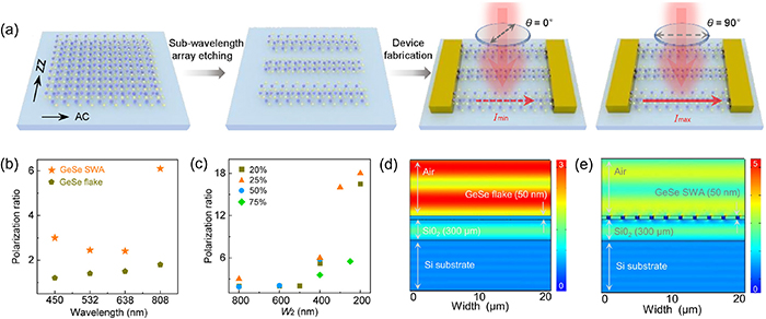
Figure 11. (a) Schematic diagram depicting the fabrication process of the GeSe sub-wavelength array photodetector and the measurement configuration. (b) Linear dichroic ratios of the pristine GeSe photodetector and the GeSe sub-wavelength array photodetector upon illuminations with various wavelengths. (c) Linear dichroic ratio as a function of period width with a series of nanostrip width/period width ratios. Calculated electric field intensity distribution of light of (d) the pristine GeSe flake and (e) the GeSe sub-wavelength array upon 800 nm irradiation. Reprinted from [264],© 2023 Science China Press. Published by Elsevier B.V. and Science China Press. All rights reserved.
Download figure:
Standard image High-resolution imageSince that the enhancement of the polarized photosensitivity in the above research is predominantly ascribed to the geometric quantum confinement, this nanopatterning strategy can thus theoretically also be applicable to other low-dimensional vdWMs. As a proof of the broad universality, in another study, Alavi et al have unveiled that the graphene nanoribbon photodetector also exhibited polarization-resolved photosensitivity [265]. The photocurrent upon linearly polarized light excitation parallel to the axial direction of nanoribbons is substantially larger than that upon perpendicular light excitation.
Nevertheless, in the previous studies, the exorbitant e-beam lithography, scanning probe lithography, and inductively coupled plasma etching techniques are entailed to prepare the nanoribbons [264, 266, 267], which severely hinders the large-scale preparation. Therefore, it is an ongoing quest to develop low-cost synthesis technique for producing vdWM nanoribbons. Regarding this pivotal scientific issue, in 2019, Watts et al presented a method for producing quantities of high-quality, individual phosphorene nanoribbons by ionic scissoring of macroscopic BP crystals [268]. In 2022, Deng et al recently reported a lithography-free synthesis technique for the preparation of high-density MoTe2 nanoribbon arrays [269]. The width of the nanoribbons is as narrow as tens of nanometers. In another study, Abu et al have synthesized phosphorene nanoribbons via an electrochemical process that utilized the anisotropic Na+ diffusion barrier along the [001] zigzag direction against the [100] armchair direction [270]. Most recently, Chen et al have reported on the preparation of h-BN nanoribbons by exploiting a Zn nanoparticle catalytic etching approach [271]. These findings have opened potentially new pathways for the implementation of low-cost and high-performance low-dimensional vdWM polarized photodetectors.
In summary, a series of strategies have been developed to enhance the degree of polarization of low-dimensional vdWM photodetectors or to induce polarization-resolved photosensitivity in high-symmetry vdWM photodetectors. For clarity, table 3 has summarized the performance metrics of related devices. It can be found that these strategies have greatly enriched the categories of polarized photodetectors and lay a solid foundation for their on-chip integration. In addition, these approaches have also provided distinctive paradigms for the further breakthroughs in the degree of polarization of low-dimensional vdWM photodetectors, enabling reliable polarized photodetection.
Table 3. A summary of the performance metrics of low-dimensional vdWM polarized photodetectors integrated with various polarization strategies.
| Devices | R (A/W) | EQE (%) | D* (Jones) | Rise/decay time | Dichroic ratio | References |
|---|---|---|---|---|---|---|
| Bi2S3 nanowire | 23 760 | 5.55 × 10⁶ | 3.68 × 10¹³ | ≈1 ms/≈4.5 ms | 2.4 | [97] |
| Core–shell SbI3/Sb2O3 heterostructure | 1.11 × 10⁻³ | 0.307 | 1.8 × 10⁹ | 19.61 ms/20.57 ms | 3.14 | [185] |
| 3D MoS2 | 23.8 | 7486 | N. A. | ≈0.4 s/≈0.04 s | 1.64 | [195] |
| BP homojunction defined by ferroelectric domains | 1.06 | 90.8 | 1.27 × 10¹¹ | 0.361 ms/0.362 ms | 288 | [208] |
| Strained MoS2 nanosheet | 3.6 | N. A. | ≈2 × 10¹¹ | 0.4 ms/0.7 ms | 2.29 | [235] |
| MoS2/CrOCl heterostructure | N. A. | N. A. | N. A. | N. A. | 1.23 | [239] |
| WSe2/CrOCl heterostructure | 5.28 | N. A. | N. A. | <0.4 ms | 1.27 | [236] |
| BP with bowtie Ti/Au antennas | 0.0142 | N. A. | N. A. | <90 μs | 8.7 | [252] |
| MoS2 with elliptical Au antennas | 26 | N. A. | N. A. | N. A. | 1.45 | [254] |
| Metamaterial-integrated graphene | 3.16 V/W | N. A. | N. A. | 25 ms/N. A. | 115 | [259] |
| Graphene on Au nanogratings | 2.95 × 10⁻³ | N. A. | 2.8 × 10⁶ | 39 ms/32.1 ms | 6.65 | [256] |
| GeSe-based SWA | 30 | N. A. | N. A. | N. A. | 18 | [264] |
a N. A.: not applicable. b The output signals of these devices are photovoltage.
6. Emerging applications
6.1. Multiplexing optical communications
Compared to the traditional polarization-insensitive photodetectors (e.g. Si, Inx Ga1−x As), which can only detect the light intensity, the polarization-discriminating photodetectors can identify more light information (i.e. both light intensity and polarization direction). In this regard, the novel optical communication systems based on polarization-resolved low-dimensional vdWM photodetectors can theoretically transmit digital information in a more efficient manner by exploiting the polarization state as the semantide.
To this end, most recently, Yi et al have implemented proof-of-concept dual-channel optical information transmission based on polarization-discriminating Bi2S3 nanowire photodetectors [97]. Basically, the polarization state and light intensity of the transmitting light are synchronously used as transmission channels for digital information, which are denoted as polarization state channel and light intensity channel, respectively (figure 12(a)). Specifically, for the Bi2S3 nanowire photodetectors, the parallel polarization state represents '1' of the binary signal, while the perpendicular polarization state represents '0' of the binary signal. On the other hand, the strong light represents '1' of the binary signal, while the weak light represents '0' of the binary signal. In this study, as an attempt, binary signal of '10011100' is used to program the light intensity, while binary signal of '00110110' is synchronously used to program the polarization state. As shown in figures 12(b) and (c), the output current of the Bi2S3 nanowire photodetector has appeared in four disparate values, which are annotated as 'level 1', 'level 2', 'level 3', and 'level 4' from low to high, respectively. This is because that the photocurrent of the Bi2S3 nanowire photodetector is closely related to both the polarization state and the light intensity. Specifically, 'level 1' can be decoupled into '0' of the polarization state channel and '0' of the light intensity channel, 'level 2' can be decoupled into '1' of the polarization state channel and '0' of the light intensity channel, 'level 3' can be decoupled into '0' of the polarization state channel and '1' of the light intensity channel, and 'level 4' can be decoupled into '1' of the polarization state channel and '1' of the light intensity channel. According to the above decoding rules, the output current signal in figure 12(c) can be decoupled into '0011011010011100' (figure 12(d)), successfully transmitting 16 binary signals in 8 readout cycles. On the whole, compared to the optical communication systems based on isotropic photodetectors, this dual-channel transmission scheme can theoretically improve the efficiency of optical information delivery by 100% without the requirement to expedite the readout speed, providing a new paradigm for high-efficiency optical transmission of binary information.
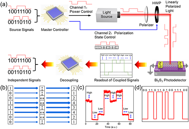
Figure 12. (a) Schematic diagram illustrating the principle of multiplexing optical communications based on a polarization-discriminating Bi2S3 nanowire photodetector. (b) Schematic diagram of the input light intensity signal and the corresponding polarization state signal from the signal output end. The  symbol represents perpendicular polarization, and the ↔ symbol represents parallel polarization. The weak light is denoted by '0', and the strong light is denoted by '1'. (c) Output current of the Bi2S3 nanowire photodetector when '10011100' and '00110110' are transmitted synchronously through light intensity channel and polarization state channel, respectively. (d) The theoretical decoupled binary signal extracted from the output current in (c). Reproduced from [97] with permission from the Royal Society of Chemistry.
Download figure:
Standard image High-resolution imageIn another study, Wang et al have developed a proof-of-concept polarization division multiplexing approach for high-efficiency optical information transmission based on a 2D γ-InSe polarized photodetector (figure 13) [272]. In brief, by dividing the information transmission channels via various polarization angles, the signal transmission efficiency can also be markedly improved without increasing the frequency of data modulation. Herein, four polarization states (polarization angles of 0°, 20°, 40°, and 60°) are exerted as the information transmission channels. Since the photoresponse of the γ-InSe polarized photodetector is related with both the polarization state and the intensity of incident light, there will in theory emerge a total of 16 distinct current values. In the receiving end, one bit of output current can be decoded into the signals of four polarization state channels, thus realizing the multiplexing optical communications.

Figure 13. Schematic illustration of the polarization division multiplexing approach for optical communications based on the polarized γ-InSe photodetectors. Reproduced from [272]. CC BY 4.0.
Download figure:
Standard image High-resolution imageDespite the pioneering progress in this research domain, it should be noted that there are still two critical issues to be addressed in terms of optical communications. On the one hand, in the modern optical communication systems, near-infrared light, including 850 [273], 1310 (O-band) [274], and 1550 nm (C-band) [275], is the most frequently used, because the transmission loss is the lowest in these wavebands. On the other hand, the current polarization-discriminating photodetectors still suffer from relatively uncompetitive linear DRs (<3) [82, 129, 172, 276], making them unqualified for meeting the ever-increasing error rate requirements of modern optical communication systems. In this regard, there is still an urgent demand to develop polarization-sensitive photodetectors with high anisotropy in the near-infrared wavebands.
6.2. Enhanced-contrast polarimetric imaging
Imaging based on semiconductor photodetectors is widely exploited in a variety of fields such as machine vision, astronomical photography, biomedical imaging, automatic drive, and security surveillance. Compared to conventional imaging techniques, polarimetric imaging offers an additional degree of freedom for modulation [81], which thus can extract features more efficiently and comprehensively. Accordingly, it has been extensively explored and applied. For example, in common strong scattering conditions (e.g. foggy, muddy, colloids, cloudy, smoky, misty, and porous media), as a result of the interaction of light with the medium, the propagation direction of light will be altered, and the scattered light will generally exhibit a high degree of polarization. In this consideration, polarimetric imaging technology can harness the polarization properties of the scattered light to enhance the contrast between the target and the background, thereby improving the reliability of target identification. Low-symmetry low-dimensional vdWM photodetectors can identify the polarization information of incident light without compromising the structural complexity and volume of the optoelectronic system, making them ideal platforms for realizing polarimetric imaging.
To this end, in 2020, Tong et al demonstrated contrast-enhanced mid-infrared polarization imaging by exploiting the polarization-discriminating quasi-2D tellurium photodetector as the crucial sensing unit (figure 14(a)) [277]. Specifically, the polarization state of the scattered light can be quantified using the Stokes vector, which is a 4D vector and can be defined as
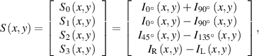
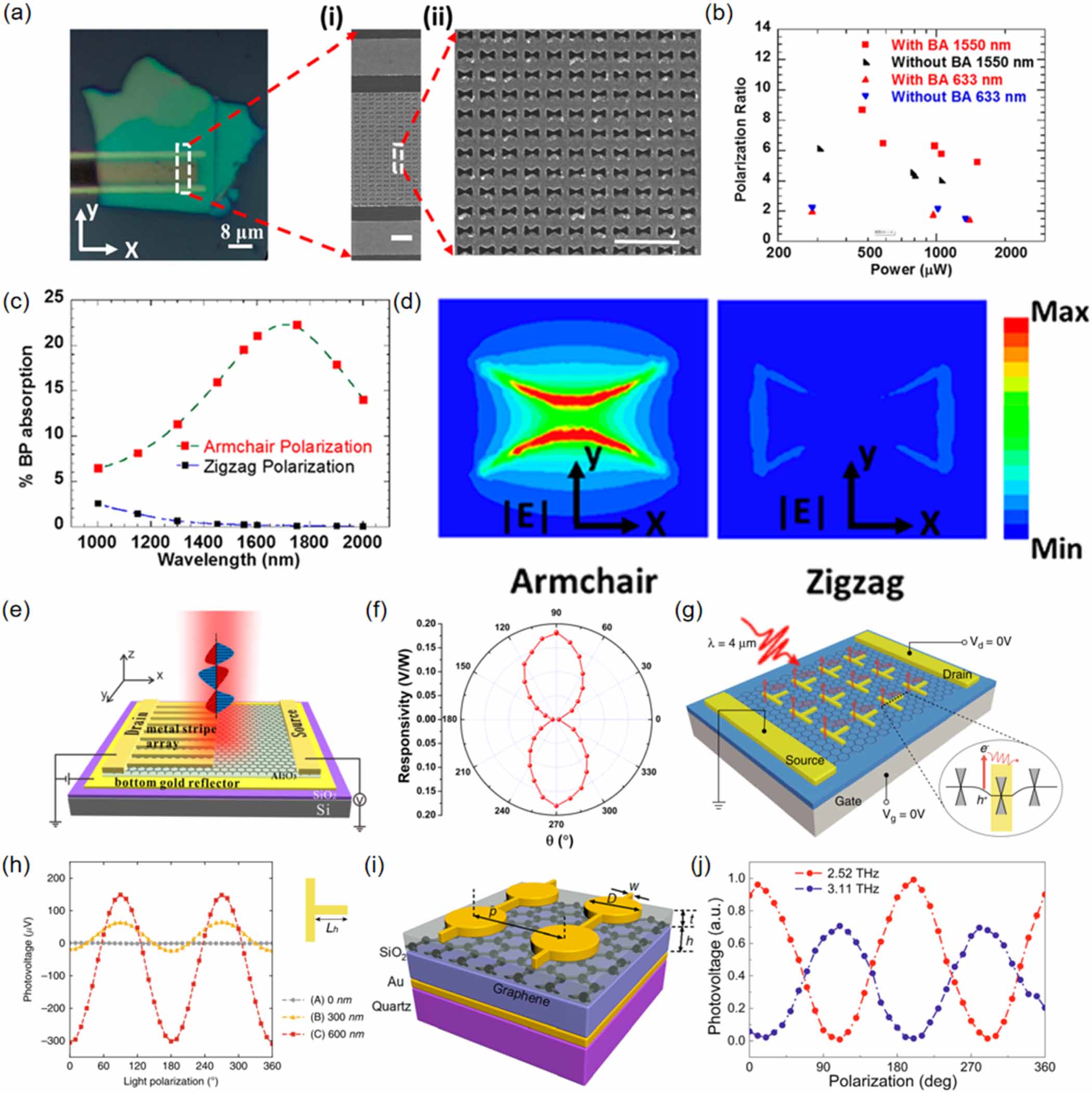
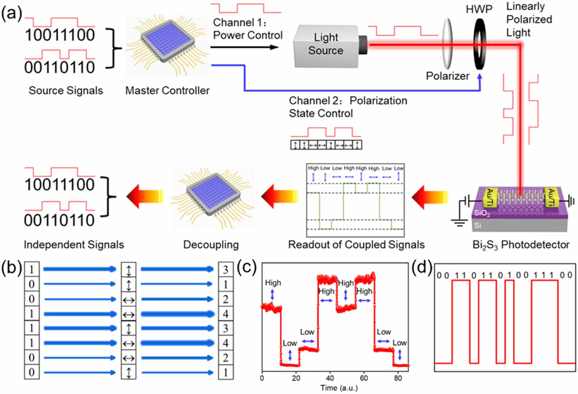
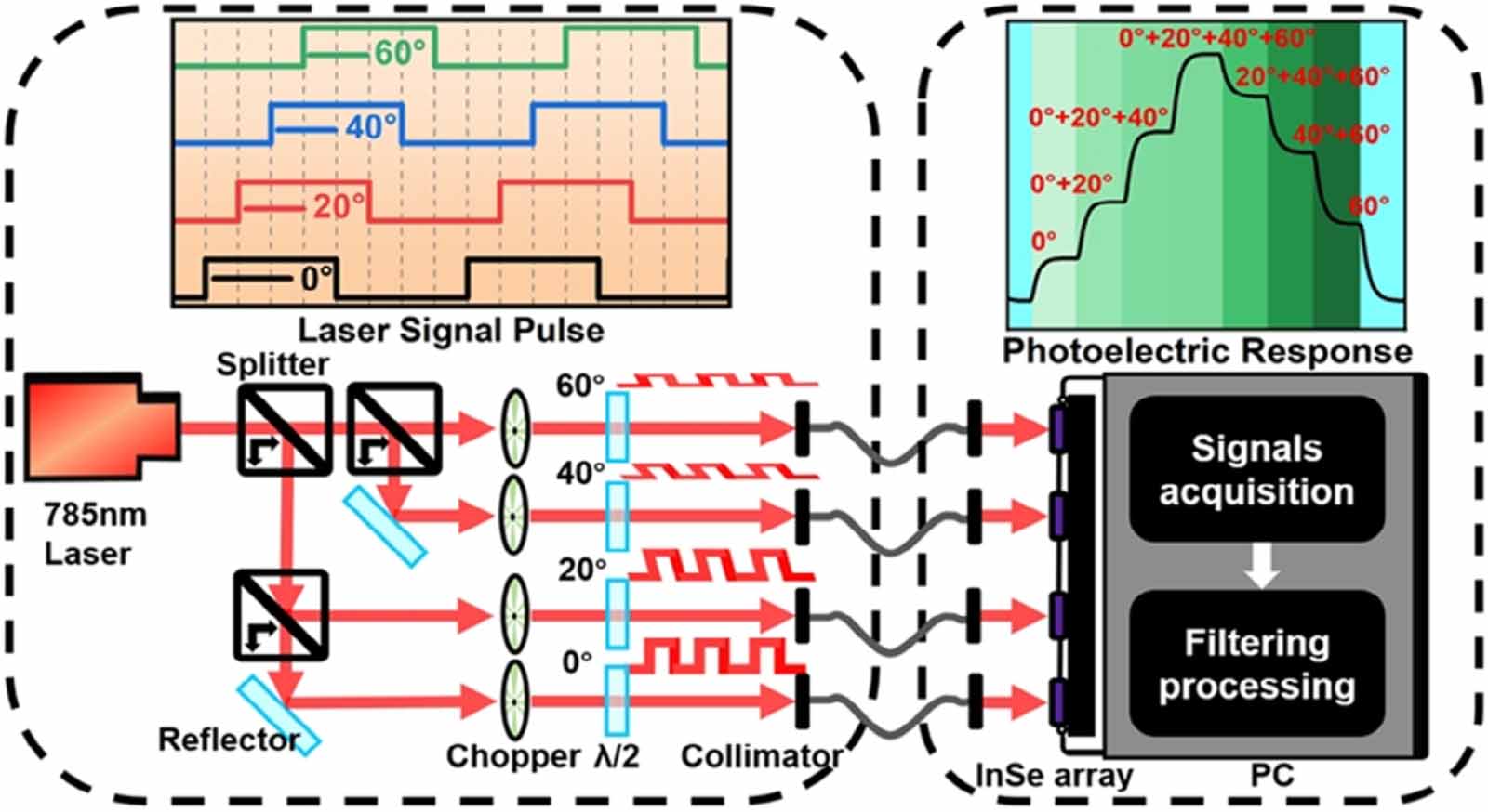
Figure 14. Contrast-enhanced polarization imaging based on Te photodetectors. (a) Schematic illustration of the imaging configuration based on a Te photodetector. (b) Schematic of the polarization imaging mechanism for extract the degree of linear polarization (DoLP). (c) Normalized imaging contrast of S0 and DoLP by using various devices as light-sensing units. (d) Imaging DoLP result using the nonpolarized 2H-MoTe2 device upon 1.55 μm illumination. (e)–(f) Imaging DoLP results using the Te photodetector upon 1.55 and 2.3 μm illuminations, respectively. Reproduced from [277]. CC BY 4.0.
Download figure:
Standard image High-resolution image
where I0° (x, y), I90° (x, y), I45° (x, y), and I135° (x, y) represent the linear polarized light intensity along the corresponding directions. IR (x, y) and IL (x, y) represent the right-handed light intensity and left-handed light intensity. That is, S0 refers to the total intensity of light, which is the intensity sum of all polarization directions and corresponds to non-polarized light. By contrast, S1 and S2 describe the information about the polarization direction of light. S3 describes the information about the rotation direction of the light vector. For linear polarimetric imaging, the information contained in S0, S1, and S2 is essential (figure 14(b)). Therefore, degree of linear polarization (DoLP) is defined according to
Figure 14(c) presents the imaging DoLP result of the isotropic 2H MoTe2 photodetector, which indicates that the contrast is inferior than the S0 imaging. By contrast, the imaging DoLP result of the 2D tellurium photodetector at the same wavelength exhibits much enhanced contrast (figure 14(d)). Moreover, a better imaging DoLP contrast has been realized upon 2.3 μm illumination, which is attributed to the larger degree of polarization at this wavelength (figures 14(e) and (f)). Following this success, in another study, Zhang et al realized a contrast-enhanced linear polarization imaging based on a self-driven polarization-sensitive PdSe2 photodetector [196]. Most recently, Kong et al have realized 78% and 112% contrast enhancement based on the imaging DoLP and imaging AoLP by using a self-driven MoTe2/MoS2 polarized photodetector as the sensing unit [278]. These pioneering achievements have demonstrated the tremendous potency of low-dimensional vdWMs toward advanced imaging techniques.
Taking a step further in the promotion of low-dimensional vdWM polarized photodetectors in practical application, Yu et al have developed a dual-band real-time object identification system based on a 2D GeSe image sensor [279]. Impressively, the recognition confidence in the hypothetical autonomous driving scenes is higher than 90%, demonstrating great potential for driverless car.
Overall, low-dimensional vdWM polarized photodetectors can detect more dimensions of incident light, thus greatly expanding their potential application scope as compared to the conventional isotropic photodetectors. In addition to the proof-of-concept multiplexing optical communications and enhanced-contrast imaging, these devices also manifest immense potential to be applied in a wealth of rapidly progressing fields such as navigation [280] and anti-counterfeit technology [281] in the future.
7. Conclusion
As a concluding remark, low-dimensional vdWMs have promised intriguing polarized photosensitivity to linearly polarized light without the involvement of intricate optical systems, which enables flexible miniaturization on a chip. In this review, we have systematically epitomized the latest advancements of polarization-resolved photodetectors based on low-dimensional vdWMs. To begin with, photodetectors built of low-dimensional vdWMs with intrinsic low symmetry, including 1D vdWMs and 2D vdWMs, have been introduced. Secondly, a variety of symmetry reduction engineering strategies for enhancing/inducing polarized photosensitive characteristics, including quantum tailoring, construction of core–shell structures, rolling engineering, ferroelectric regulation, strain engineering, integration of low-symmetry optical antennas, nanopatterning regulation, etc, have been comprehensively surveyed. The emphasis has been focused on the underlying working principles, providing new pathways for improving the degree of anisotropy of low-dimensional vdWM polarized photodetectors. Finally, we have underscored a series of emerging applications based on low-dimensional vdWM polarized photodetectors, such as dual-channel optical communications and polarized imaging with enhanced contrast, which bring these devices into full play and provide navigations for the upcoming research efforts toward the future commercialization of the corresponding optoelectronic devices. On the whole, this review aims to provide researchers, especially the abecedarians, with a rapid and comprehensive understanding on the domain of low-dimensional vdWM polarized photodetectors, and to contribute to the further development of the integrated on-chip polarized optoelectronics industry.
8. Future perspectives
8.1. Optoelectronic anisotropy of novel low-dimensional vdWMs and large-area device integration
Thus far, there have emerged thousands of vdWMs and related heterostructures [10, 282–286], a substantial portion of which possess relatively low crystal structure symmetry. However, only less than 100 vdWMs' anisotropic photosensitive properties have been systematically explored. In this consideration, the polarization-dependent photosensitivity of photodetectors built of novel low-symmetry vdWMs (e.g. MoI3 [79], Nb2Se9 [287], α-Bi4Br4 [117], Ta2Ni3Se8 [288], GePdS3 [58], CrSbSe3 [289], BiSeI [290], Ta2Se3 [291], AsSbO3 [292], AsSbS3 [293], [BiSbS3]2 [Te2] [294]) is still an intriguing research subject to be investigated. An ineluctable challenge prior to practical commercialization is the large-area fabrication of these low-dimensional vdWMs. Thus far, molecular beam epitaxy [295], metal-organic chemical vapor deposition [296], chemical vapor deposition [297], and pulsed-laser deposition [118] have proven as compelling strategies for synthesizing large-area 2D materials. These techniques can be further developed for preparing various 2D vdWMs in the future. As for the 1D vdWMs, Wei et al have recently developed a nanoscale grooves-induced unidirectional growth scheme for preparing oriented 1D Te nanowires [93]. Since this technique relies mostly on the morphology of the substrate, it can thus theoretically be extended to the growth of other 1D vdWMs, which is in need of further exploration.
8.2. Development of new polarization strategies
Thus far, only a handful of polarization approaches on low-dimensional vdWMs have been experimentally proved. From a fundamental perspective, any strategy that can reduce the overall symmetry of the devices can induce/enhance the polarized photosensitive characteristics of low-dimensional vdWM photodetectors. Thus far, researchers have developed a series of new approaches to deteriorate the overall symmetry of the vdWM devices, such as dielectric engineering [34], rippling engineering [298], etc. It can be conceived that these approaches can theoretically be applied to ameliorate the optoelectronic anisotropy of low-dimensional vdWM polarized photodetectors, providing alternative avenues for the implementation of advanced polarized optoelectronics. Moreover, in addition to the linear polarization state, the identification of circular polarization state is also critical. As a pioneering attempt, Wei et al have put forward a distinct paradigm of geometric photodetectors realizing a substantial discrimination ratio of 84 and a detectivity of ellipticity down to 0.03° Hz−1/2 [299]. In another study, Bu et al have achieved ultrahigh light ellipticity discrimination in a monolithic ultracompact circular polarization detector based on a configurable circular-polarization-dependent optoelectronic silent state with zero photocurrent and markedly suppressed noise [300]. Since the introduction of new functions relies only on the geometric designs, these schemes in theory can be exploited to other low-dimensional vdWMs with various electronic structures toward the detection of circular polarization state in various wavebands.
8.3. Polarizing polycrystalline low-dimensional vdWMs
Currently, the vast majority of polarization strategies have been only applied to monocrystalline low-dimensional vdWMs. Compared to low-dimensional single crystals, the preparation of polycrystalline vdWMs is much simpler and more cost-efficient, especially in terms of the scalable production. As proof, the wafer-scale preparation of polycrystalline Te [301], HfSe2 [295], WTe2 [302], NbSe2 [303], h-BN [304], and even the ZnIn2S4/SnS van der Waals heterostructures [30] has been realized. Nevertheless, due to the mutual cancellation of the anisotropy of domains with arbitrary orientations, the overall symmetry of the polycrystalline system is generally improved. As a consequence, photoelectric devices built of polycrystalline vdWMs typically exhibit isotropic photoresponse [22], despite that the photosensitive materials host intrinsic anisotropic lattice structures. It is worth emphasizing that most polarization strategies do not fundamentally rely on the crystallinity of the photosensitive materials. For example, rolling engineering [195] and nanopatterning regulation [264] only rely on the extrinsic geometry of the photosensitive materials, and they are thus independent on the crystallinity. In this regard, theoretically, these polarization strategies are universal, and they can also be exerted for polarizing polycrystalline vdWMs. However, there has by far been little progress on the exploitation of these strategies to polycrystalline vdWMs toward polarized photoelectric detection. In the upcoming future, this subject is worthy of more research enthusiasm, and the related advancements will open up vast opportunities for low-cost scaled-up production of polarized photodetectors.
8.4. Integration of multiple polarization strategies
Thus far, although a series of polarization strategies have been developed and applied to induce polarity/enhance the degree of anisotropy of low-dimensional vdWM photodetectors, their linear DRs are still relatively low (<10), making them unqualified for fully meeting the various tangible applications. Of note, the basic principles of the polarization strategies mentioned above are distinct, and their practical implementation relies on the regulation of different components of the optoelectronic devices. For example, polarization strategies such as quantum tailoring [97], rolling engineering [195], and nanopatterning regulation [264] are implemented based on the reduction of the overall geometric symmetry of the photosensitive channels. By contrast, integration of low-symmetry optical antenna [259] and ferroelectric engineering [208] are achieved by reducing the geometric symmetry of the external environment in vicinity of the photosensitive channels. Therefore, these strategies can theoretically be applied simultaneously to polarized photodetectors to synergistically leverage the optimal polarization photosensitive characteristics, which portends a promising solution for further breakthroughs in the future.
8.5. Developing novel applications based on low-dimensional vdWM polarized photodetectors
The past decade has witnessed the successful exploration of low-dimensional vdWMs for various prototypical polarization-sensitive photodetectors. However, in order to promote these devices for widespread commercialization, it is necessary to develop more applications with these devices as the pivotal functional units, such as polarization navigation [280], polarized anti-counterfeit technology [305], medical diagnosis [306, 307], LiDAR [308], encrypted communications [309, 310], etc.
8.6. Boosting the photosensitivity
An ongoing challenge of low-dimensional vdWM photodetectors is their low photosensitivity, which is largely originated from the weak light absorption induced by the atomic-scale channel thickness, the strong interfacial effects, and the short carrier lifetime induced by the strong spacial confinement. To address these issues, researchers have developed numerous strategies for performance improvement, including integration of optical waveguide/optical cavity/plasmonic optical antennas [311–313], dielectric engineering [34], strain modulation [241], surface modification [314], substrate passivation [315], etc. In principle, these strategies can be compatible with various low-dimensional semiconductors and polarizing approaches. Therefore, these techniques can be developed for ameliorating the photosensitivity of the low-dimensional vdWM polarized photodetectors. Further research is demanded to determine whether these technologies will have an impact on the polarization characteristics. The aim is to improve the photosensitivity without compromising other performance metrics such as the DR.
Acknowledgments
This work is supported by the National Natural Science Foundation of China (Grant Nos. U2001215, 52272175), the Natural Science Foundation of Guangdong Province (Grant Nos. 2021A1515110403, 2022A1515011487), the Science and Technology Projects in Guangzhou (Grant No. 202201011232), the One-Hundred Talents Program of Sun Yat-sen University, and State Key Laboratory of Optoelectronic Materials and Technologies.
Conflict of interest
There are no conflicts to declare.
Author contributions
Conceptualization: J Y and G Y; Data curation: Y M, H Y, W W, and H L; Funding acquisition: J Y, and G Y; Project administration: J Y and G Y; Resources: J Y and G Y; Supervision: J Y and G Y; Visualization: Y M and H Y; Writing—original draft: Y M, H Y, and H L; Writing—review & editing: J Y All authors have approved the final version of the manuscript.