

Abstract
We report on a combined atomic force microscopy, Raman spectroscopy, and transmission electron microscopy study of InAs/Al(Ga)As and AlAs/InAs quantum dot nanostructures grown by molecular beam epitaxy in the Stranski–Krastanov growth mode on (001)-oriented GaAs substrates. Structure periods of 50 nm and 100 nm were determined by atomic force microscopy of cleaved as well as ion-milled sample surfaces and were confirmed by high resolution transmission electron microscopy. Spatially resolved Raman spectroscopy analysis of a beveled surface allows profiling the Raman intensity of phonon modes. An optimal access to the spatially dependent changes in the phonon spectra is achieved by polishing the samples at an angle of 5–7 degrees with respect to the original sample surface plane. Such analysis allowed the localization of individual quantum dot layers. This opens a way to the structural characterization of quantum dot multilayers by the combination of atomic force microscopy and Raman spectroscopy.
Export citation and abstract BibTeX RIS
1. Introduction
InAs quantum dots (QD) are currently used in optoelectronic devices such as photodetectors, high temperature lasers, and single photon sources [1, 2] and considered also as a promising system to improve the efficiency of III–V solar cells [3]. Most of these applications use InAs QDs in a GaAs matrix as an active material, which yields interband energies in the range of 1.2–1.4 eV (850–1000 nm) [4], i.e. in the infrared region. However, using InAs embedded in an AlAs matrix allows the InAs QD interband energy to be tuned in the range of 1.8–2 eV (620–690 nm) [5], i.e. in the visible range, which is preferable for optoelectronic applications. This shift results from the higher confinement potential of AlAs (band gap of 2.16 eV as compared to 1.42 eV for GaAs) and the smaller size of InAs QDs [6, 7] formed in an AlAs matrix.
Despite its technological and fundamental potential, the InAs/AlAs system is poorly studied in comparison to the InAs/GaAs one. Regarding device fabrication and optimization, the key factor is extracting information about the structural and optical properties of the QDs, including morphology and phonon properties, which govern electron scattering in realistic nanostructures. The majority of devices are formed of multilayers, namely QD layers, matrix layers, and a protective capping layer. For InAs/Al(Ga)As based systems, a capping layer is required in order to protect the matrix from oxidation [8, 9]. It was shown, however, that covering the QDs with a capping or matrix layer can modify their morphology and, therefore, optical properties [10–12].
There are several microscopic techniques capable of directly probing the QD size and morphology. One of the most powerful techniques is transmission electron microscopy (TEM), which allows QDs to be investigated both in planar and cross-sectional views. It provides excellent resolution, but requires sophisticated sample preparation and high-vacuum (HV) conditions. Another technique is cross-sectional scanning tunneling microscopy (STM), which provides rich information on QD composition, shape, lattice parameter, and strain distribution with atomic resolution [13]. However, STM can be applied only to conductive samples, which limits its application, and UHV conditions are preferred to prevent surface oxidation. Atomic force microscopy (AFM), as compared to the methods mentioned above, operates at ambient conditions. AFM allows one to perform size and morphology analysis of QDs from planar surfaces on freshly grown samples without capping layers [6, 7]. For As QDs embedded in Al(Ga)As the structural parameters, which are different from those of free-standing QDs, can also be studied by AFM from a cleaved {110} plane. Cleavage is a simple and well-established method for sample preparation, which can provide atomically flat surfaces and precludes unintended diffusion [13]. AFM was already used for the visualization of layers in GaAs/Al(Ga)As multi-quantum well structures using selective etching [14]. It was also established that some III–V materials readily oxidize, forming topography patterns on the surface of multilayer structures. For GaAs/A1xGa1−xAs and GaAs/GaInP heterostructures the oxidation rate depends on the layer composition [15, 16]. The drastically different oxidation rates of GaAs and AlAs were applied by the group of Gonnelli [17] for a very precise determination of the layer thicknesses in GaAs/AlAs multilayers. The surface profile of unoxidized heterostructures can be probed by AFM since it is determined by the strain relaxation of QDs on a cleaved surface, as was shown for SiGe QDs by Dunaevskii et al [18].
An alternative way of sample surface preparation for AFM characterization where cleaving is not possible is ion milling. This method has been used successfully for the preparation of SEM [19] and TEM [20] samples. Even brittle materials or very different material combinations can be easily prepared by this method. Ar+ ion milling can achieve sample surfaces of very high quality [21]. Ion beam cutting at an angle in combination with chemical etching was used by Robson et al [22], who observed AlxGa1−xAs/GaAs layers as thin as 1 nm with AFM.
Complementary to direct structural imaging, non-destructive optical methods, such as photoluminescence, ellipsometry Raman, and infra-red spectroscopies, are widely applied to study nanostructures, including superlattices and quantum dots [23]. Raman spectroscopy allows not only structural parameters such as superlattice periodicity and layer composition to be determined, but also provides information on electronic, optical, and phonon properties of the structures [24]. Raman spectroscopy has been extensively applied for the study of multilayer In(Ga)As/Al(Ga)As QD structures, atomic intermixing [25, 26], the QD size [27], shape [27], and strain relaxation [28].
Micro-Raman scattering can be used to extract depth profiles of semiconductor layered structures [29]. Raman scattering from planar surfaces allows the depth from which the signal is acquired to be chosen by a confocal micro-Raman setup [29]. The depth profile can also be extracted by scanning over the sample cross-section. The resolution achieved depends on the excitation light wavelength and the objective used and can be as small as 0.3 μm [30, 31]. Much smaller layer thicknesses can be determined by scanning beveled samples [31, 32]. This approach was used to identify the location and the doping profile of δ-doped GaAs with a resolution as good as 10 nm [33]. Profiling of strain, Ge composition, and defects with a resolution of 15 nm was reported for beveled Si/Si1−xGex/Si heterostructures [32]. The space charge width of 100 nm at ZnSe/GaAs interface was determined from the line-shape analysis of the coupled LO phonon-plasmon mode [33].
In this paper we discuss approaches for the depth profiling of InAs QD multilayer structures incorporated in AlAs or Al0.75Ga0.25As matrices, as well as of inverted structures (AlAs QDs in InAs matrix) using atomic force microscopy, Raman spectroscopy, and transmission electron microscopy aiming at localizing single QD layers.
2. Experimental details
2.1. Quantum dot growth
The samples under investigation were grown on epi-ready n+ Si-doped (NSi = 3 · 1018 cm−3) or semi-insulating (001)-oriented GaAs substrates using a solid-source molecular beam epitaxy system Riber 32P. The substrates were first degassed for 40 min at 623 K and then loaded directly into the growth chamber. After the native oxide layer was desorbed by annealing the substrates at 883 K for 2 min, a Si-doped GaAs buffer layer of 200–1000 nm was grown at a rate of 1.0 monolayer per second (ML s−1) at 853 K under a constant As beam equivalent pressure (BEP) of 1 · 10−5 Torr. The samples investigated consist of multilayers containing AlAs and InAs QDs embedded in InAs and Al(Ga)As matrices, respectively. The growth of the QDs was monitored by reflection high energy electron diffraction (RHEED). According to RHEED data the transition from a two-dimensional to a three-dimensional growth mode (beginning of island formation) for all samples occurs after the deposition of 1.8 MLs of the island material. The total amount of both InAs and AlAs was 2.2 to 2.4 MLs for the QD growth. The substrate temperature was 733 K (773 K) during the growth of AlAs (InAs) QDs in the InAs (AlAs or AlGaAs) matrix at an arsenic BEP of 8 · 10−6 Torr. The growth interruption after QDs formation ranges from 12 s for the AlAs QDs to 50 s (sample A) and 150 s (samples B and C) for the InAs ones. The first 5 nm of AlAs or AlGaAs spacers were grown at the same temperature as the QDs (773 K); then the temperature was raised to 883 K and the rest of the AlGaAs spacer was deposited. All InAs/Al(Ga)As structures were covered by a 40 nm GaAs capping layer. The exact structure for each sample is defined in figure 1.
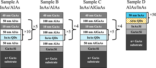
Figure 1. Structure of the samples with InAs and AlAs QDs in Al(Ga)As and InAs matrices, respectively.
Download figure:
Standard image High-resolution image2.2. Sample preparation
Sample preparation for AFM measurements included either cleaving or ion beam slope cutting. Cleaving was performed for InAs/AlAs QD multilayers by pressing the edge of the sample with a diamond cutter from the back side resulting in atomically flat surfaces extending along the  direction.
Ion beam slope cutting (ion milling) was implemented for the AlAs/InAs QD system since cleaving was not possible due to defects in the matrix material caused by the large lattice mismatch between the InAs matrix material and the GaAs substrate. Before ion cutting, the samples were cleaned with ethanol in an ultrasonic bath and then mounted on a sample holder with Crystalbond™ glue by heating up to about 393 K. During the milling process the sample surface was partly protected by a sharp edged mask. This protective mask (thin cover slip) was glued to the sample by heating up to 393 K for about 1 h and the sample was cut with a diamond wire saw. Finally, the sample was cleaned in an ultrasonic bath with acetone to remove any remaining Crystalbond™ glue. The unprotected part of the sample was milled by a high-energy Ar ion beam. Ion beam slope cutting was performed with a Leica EM TIC 3X milling system. Instead of one ion beam and sample oscillation, the system uses three ion beams hitting the sample from 3 different directions (figure 2). The result is a flat and polished surface, as is confirmed by AFM. Milling was performed at an ion energy of 6 keV at room temperature as well as with nitrogen cooling at 193 K and 143 K.
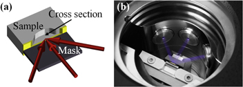
Figure 2. Triple ion beam technique for ion beam slope cutting: (a) schematics of the experiment, (b) the overview of the sample chamber in the ion beam slope cutting setup.
Download figure:
Standard image High-resolution imageBeveled samples were prepared by mechanically polishing the samples at an angle of 5 to 7 degrees with respect to the plane of the layers. The sample is first cleaned in acetone and glued on glass with cyanoacrylate adhesive Sicomet8300™. The glass is displaced from the edge of interest. Then the sample is glued on a sample holder and heated at 353 K for 30 min. Subsequent polishing in water is performed with diamond foils (ultraPrep™ Diamond Lapping Films, Buehler) sequentially decreasing the grain size (3, 1, 0.5, and 0.1 μm). The quality of the beveling was controlled with an optical microscope. Finally the glue was dissolved in acetone.
The tilt angle was measured with an optical microscope from the width and depth of the beveled structure. For the Raman experiment the sample was glued on a sample holder prepared at a predefined angle. The schematics of AFM and Raman experiments with samples prepared by the methods mentioned above are shown in figure 3.
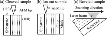
Figure 3. Schematics of the AFM (a), (b) and Raman (c) experiments. Dotted lines indicate QD layers embedded in the matrix.
Download figure:
Standard image High-resolution image2.3. TEM, AFM and Raman measurements
The high resolution TEM (HRTEM) investigation of (110) cross-section samples were made by means of JEOL-4000EX and FEI TITAN 80–300 microscopes operating at 400 and 300 kV, respectively. Conventional two-beam {002}-dark-field diffraction contrast was applied to characterize the spatial distribution of QDs and structural defects. The morphology and atomic structure of QDs were investigated in the multi-beam HRTEM mode.
AFM measurements were performed in intermittent mode with an Agilent 5420 system using NSC14 general purpose Si tips from Mikro-Mash with nominal tip radius and force constant of 8 nm and 5 N m−1, respectively.
Micro-Raman spectra were acquired with a confocal Horiba JY HR800 spectrometer using 514.5 nm (Ar+ laser) and 514.7 nm (solid state Cobolt laser) excitation wavelengths at a power of 0.1–0.5 mW and a spectral resolution of 2.5 cm−1. The laser was focused on the sample via an Olympus BX41 microscope using a 100x objective to the spot of approximately 500 nm radius. Micro-Raman spectra from cleaved and ion beam cut samples were recorded from the {110} plane  with unpolarized light. Line scans on mechanically polished samples were performed in
  configuration with a Marzhäuser microscope scanning stage and a step width of 100 nm. Here and further
  refer to directions parallel to the [100], [010], [001], [1–10], [110], respectively. The sign '–' means that unpolarized scattered light was analyzed.
3. Results and discussion
3.1. TEM images
The cross-sectional dark field TEM images in figure 4 show a general view of the whole layer sequence of sample C, while HRTEM images demonstrate individual QDs in samples B, C, and D. The layer sequence and the layer thicknesses of the periodical structures determined from TEM measurements correspond to the nominal values reported in figure 1. InAs/Al(Ga)As QDs reveal a characteristic lens-like shape and have relatively high base size of about 50 nm, and height of 15 nm for InAs QDs in AlAs matrix, or 25–30 nm QD base size and 8 nm height in Al0.75Ga0.25As matrix. The presence of a wetting layer is observed in all samples. The inverted structure shows the formation of much smaller QDs with 3–5 nm base size.
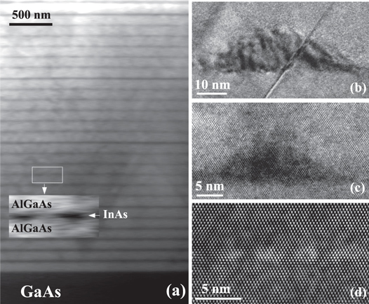
Figure 4. (a) Dark field TEM image of QD multilayer structures (sample C). HRTEM images of (b) InAs QD in AlGaAs matrix (sample C), (c) InAs QD in AlAs matrix (sample B), and (d) AlAs QD in InAs matrix (sample D).
Download figure:
Standard image High-resolution image3.2. AFM measurements
AFM images of cleaved InAs/Al(Ga)As samples presented in figure 5 allow the periodical layer structure of the samples to be visualized. The dark flat area always corresponds to the substrate, which demonstrates very good surface quality obtained by the cleavage technique. The periodic structure seen in the AFM surface topographies and, more clearly, in the amplitude mapping represents the QD multilayers, with Al(Ga)As matrix rising above the substrate level, and grooves indicating the positions of QD layers (marked by dashed lines) and of a GaAs interlayer (marked by a solid line). The interlayer distances obtained from the AFM images correspond to the nominal thicknesses of the layers given in figure 1 and confirmed by TEM experiments (figure 4(a)). As can be seen in the AFM height profiles shown in figures 5(c)), (f), and (i), AlAs rises as much as 15–30 nm above the substrate level. Even though AlAs has a smaller lattice constant than InAs, the freshly cleaved AlAs immediately oxidizes in air [8, 16], and the thickness of the aluminum oxide will increase 1.8 times with respect to the initial thickness of AlAs [8]. This leads to the observed rise above the substrate level. The Al0.75Ga0.25As matrix, due to the presence of Ga atoms, is much less prone to oxidation than pure AlAs. This leads to the formation of a 1 nm step at the edge between the substrate and the quantum dot multilayers, which is in excellent agreement with AFM observations reported elsewhere [16].
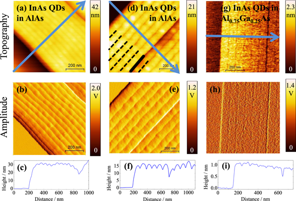
Figure 5. AFM images (surface topography and amplitude) and corresponding topography profiles of cleaved InAs/Al(Ga)As samples. Each column represents topography (top), amplitude (middle), and topography profile (bottom) along the blue arrow in the topography image. Being sensitive to the topography gradient, the amplitude image highlights surface features. (a)–(c) sample A (InAs/AlAs, 50 nm period); (d)–(f) C (InAs/AlAs, 100 nm period); (g)–(i) D (InAs/AlGaAs, 100 nm period).
Download figure:
Standard image High-resolution imageAFM images of the ion-milled AlAs/InAs QD structures prepared at different temperatures are represented in figure 6. As can be seen, after ion milling the sample surface exhibits periodic structures emerging above the matrix, which can be interpreted as oxidized AlAs QD layers since their period is equal to the nominal one (figure 1). Cooling was employed in order to minimize expected sample damage by Ar+ ions. The preparation at 193 K gives results similar to those obtained at room temperature, while at 143 K the height of AlAs QD layers is not sufficient to be clearly detected over the matrix (surface roughness is 0.1 nm, which is close to the noise limit of the AFM). Therefore, it is very likely that ion milling at higher temperatures leads to a more pronounced amorphisation of sample surface, resulting in intensive subsequent oxidation in ambient conditions. This statement is confirmed by the Raman spectroscopy analysis, which is very sensitive to the quality of the crystalline structure and to the presence and amount of defects.
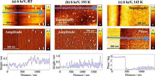
Figure 6. AFM images and topography profiles of ion-milled AlAs/InAs samples prepared at 6 keV ion energy for different preparation temperatures: (a) 296 K; (b) 193 K; (c) 143 K. Amplitude or phase image in the middle row is given for a more clear view of the periodic structure of the samples. The bottom row presents the background corrected topography profiles (phase profile for c).
Download figure:
Standard image High-resolution image3.3. Raman spectroscopy
The Raman spectra for cleaved and ion-milled samples are given in figure 7. According to Raman selection rules [36], in the backscattering geometry from {110} plane ( geometry) only transverse optical (TO) modes are allowed, while longitudinal optical (LO) modes are symmetry forbidden. Indeed, for the InAs matrix the TO phonon mode observed at about 215 cm−1 dominates the Raman spectra, while for the AlAs QDs the intensity of the TO phonon peak observed at 339 cm−1 is weaker as compared to the LO phonon mode at 366 cm−1. The latter observation can be explained by the lifting of Raman selection rules in AlAs QDs due to breaking of translational symmetry. Forbidden LO modes of the InAs matrix are observed at 237 cm−1. The frequencies of the AlAs QD phonons are shifted to lower frequencies with respect to the bulk values (from 402 cm−1 to 367 cm−1 and from 360 cm−1 to 337 cm−1 for LO and TO phonons, respectively). The downshift is attribuited to tensile strain in the QDs due to lattice mismatch [27, 34], and diagonal strain components can be estimated to be equal to
  and
and  [34]. In addition to the first-order Raman scattering, the second-order phonon modes of InAs are observed in the range from 400 to 500 cm−1. The compound overtones arise from the combinations of optical phonons of InAs (denoted in figure 7 as 2TO, 2LO, LO + TO, and TO + SO). The nature of the shoulder at 445 cm−1 is not obvious and may originate from third-order Raman scattering process. The overtone frequencies to a good accuracy (no worse than 3 cm−1) equal a sum of the corresponding values of the vibrational modes of first-order scattering. Normalized Raman intensities and full width at half maximum (FWHM) of the observed lines change depending on the preparation method and temperature. As can be seen from figure 7, the intensity of the forbidden InAs LO peak is increasing with preparation temperature for ion-milled samples as compared to the cleaved one due to relaxation of selection rules, which may be induced by defects. However, since the laser energy is close to the E1 transition is InAs [35], this effect may be caused by the change in the Fröhlich interaction, or electric field induced Raman scattering due to the Ar ion milling process. The intensity increase is accompanied by the apparent asymmetric broadening of the TO mode (from 7.3 cm−1 for a cleaved sample to 10.4 cm−1 for ion milled samples) and a slight downshift of the LO and TO modes of InAs matrix (from 217 cm−1 to 216 cm−1) due to an asymmetric phonon state density in partially amorphized InAs matrix layers [35] or/and q-vector relaxation [36]. This is confirmed by the decrease in intensity of the InAs combinational modes. Smearing out of AlAs features upon ion milling is most probably due to stronger oxidation of AlAs as compared to the cleaved sample. However, is is worth mentioning that the increase of the 'prohibited' LO feature of InAs related to the increased damage should not obligatorily be accomplished by decreasing combinational modes because of the varying resonant conditions for the observation of the combinational modes in the damaged samples.
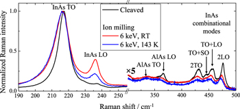
Figure 7. Comparison of normalized Raman spectra of ion milled and cleaved AlAs/InAs samples evidencing sample damage introduced by ion milling. The Raman intensity of the modes above 300 cm−1 is multiplied by 5 for better visibility. The difference in FWHM and peak position of the InAs TO phonon band for ion cut samples is comparable to the experimental error.
Download figure:
Standard image High-resolution image3.4. Raman profiling
Profiling of individual QD layers in the multilayer structure with the period of 50–100 nm from the cross-section by means of micro-Raman scattering fails since the period is much smaller than the laser wavelength used in the experiment, and thus than the lateral resolution. Therefore, Raman profiling of QD samples beveled at an angle of 5–7 degrees with respect to the (100) sample plane was employed. In this case, the effective period of the multilayer structure increased from 100 nm to 1 μm, which is well above the lateral resolution and enables the micro-Raman profiling and even optical microscopy imaging.
The representative spectra of the beveled QD multilayers are shown in figure 8. In the case of InAs/AlAs QD multilayers (figure 8(a)) very pronounced peaks of AlAs (AlAs LO and AlAs TO) are detected from the matrix. Note that in this geometry the LO mode is allowed by Raman selection rules. Therefore, the AlAs LO peak intensity is followed to obtain a Raman profile. The small intensity of the InAs QD signal and its proximity to that of As clusters appearing due to the polishing procedure obscures the direct observation of the QD layer location. GaAs LO and TO peaks originate from the GaAs interlayers. For InAs/AlGaAs QD multilayers (figure 8(b)) the matrix signal is represented by AlAs-like and GaAs-like peaks in the region between 350 and 400 cm−1 and between 250 and 275 cm−1, respectively. The AlAs-like LO peak position is downshifted by 8 cm−1 with respect to the peak positions of pure material, while the GaAs-like LO is downshifted by 27 cm−1, which corresponds to (0.70 ± 0.05) fraction of Al [37]. This value is in good agreement with the nominal alloy composition of 0.75 Al content. The InAs QD signal is relatively strong, but its proximity to the GaAs-like modes makes it unsuited for profiling. The GaAs LO mode originates from the GaAs interlayers.
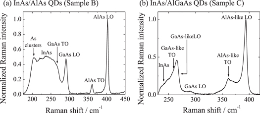
Figure 8. Typical Raman spectra of beveled (a) InAs/AlAs (sample B) and (b) InAs/AlGaAs (sample C) QD multilayers. The spectra are averaged over four points.
Download figure:
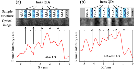
Standard image High-resolution imageThe optical images of one single stack (five layers of QDs separated by 100 nm matrix layers) of the beveled InAs/Al(Ga)As QD structures and their Raman profiles are shown in figure 9. The Raman profiles represent the obvious intensity oscillations of AlAs and AlAs-like phonon modes in InAs/AlAs and InAs/Al(Ga)As structures, respectively. The positions of the maxima of the signal approximately correspond to the center of the matrix layers, while minima indicate the location of individual QD layers. Since AlAs has a low absorption coefficient in the spectral range studied, one could expect multiple reflections to take place giving rise to interference effects. However, in our case, the interference effects are negligible due to the incorporation of InAs QD layers, which are composed of highly absorbing material.
Figure 9. Schematic structures, optical images, and Raman intensity profiles of one single stack of (a) InAs/AlAs QD and (b) InAs/AlGaAs QD structures. Schematics of the sample structure: grey areas—GaAs interlayers; white—Al(Ga)As matrix. Vertical arrows indicate the position of InAs QD layers.
Download figure:
Standard image High-resolution image
4. Conclusion
AFM and Raman spectroscopy from cleaved, ion-milled, and beveled surfaces allow individual QD layers in multilayer InAs/Al(Ga)As QD structures to be visualized. In cleaved samples, AFM benefits from the different oxidation rates of QD and matrix materials. This leads to a pronounced topography profile in InAs/Al(Ga)As as well as in AlAs/InAs QD structures prepared by ion milling. Ion milling allowed samples suitable for AFM profiling to be prepared for which cleaving was not possible. Following the intensity oscillations of Raman modes when scanning across the sample structure in beveled multilayer samples, the period of these oscillations was found to correspond to the effective period of the beveled QD structures.
The combination of AFM with Raman spectroscopy opens perspectives for nano-Raman characterization of single nanostructures by tip-enhanced Raman scattering (TERS).
Acknowledgment
This study was partially supported by the Russian Science Foundation (Grant No. 14-12-01037), Russian Foundation for Basic Research (RFBR, 13-02-12124 ofi_m) in the part of TEM investigation, the Ministry of Education and Science of the Russian Federation, DFG (project ZA146/22-1 and IRTG Grant No. GRK 1215).