


Abstract
Growth of nanocrystalline graphene films on (6√3 × 6√3)R30°-reconstructed SiC surfaces was achieved by molecular beam epitaxy, enabling the investigation of quasi-homoepitaxial growth. The structural quality of the graphene films, which is investigated by Raman spectroscopy, increases with growth time. X-ray photoelectron spectroscopy proves that the SiC surface reconstruction persists throughout the growth process and that the synthesized films consist of sp2-bonded carbon. Interestingly, grazing incidence x-ray diffraction measurements show that the graphene domains possess one single in-plane orientation, are aligned to the substrate, and offer a noticeably contracted lattice parameter of 2.450 Å. We correlate this contraction with theoretically calculated reference values (all-electron density functional calculations based on the van der Waals corrected Perdew–Burke–Ernzerhof functional) for the lattice parameter contraction induced in ideal, free-standing graphene sheets by: substrate-induced buckling, the edges of limited-size flakes and typical point defects (monovacancies, divacancies, Stone–Wales defects).
Export citation and abstract BibTeX RIS

Content from this work may be used under the terms of the Creative Commons Attribution 3.0 licence. Any further distribution of this work must maintain attribution to the author(s) and the title of the work, journal citation and DOI.
1. Introduction
Graphene is considered to be of great importance for future device applications due to its outstanding electronic properties [1]. Regarding its synthesis, several techniques have been used for the production of this material [2–9]. Among them, micro-mechanical cleavage of graphite [4], which allows for the preparation of flakes with different numbers of graphene layers and high structural quality, is certainly the most popular. However, in spite of being very useful for the preparation of graphene aiming at basic research, this method is unsuitable for industrial applications. On the other hand, techniques such as surface thermal decomposition of SiC [5, 6] and chemical vapor deposition (CVD) on metallic templates [7, 8] are promising due to their capability of achieving large-area synthesis. Despite this advantage, they also have inherent drawbacks. With Si depletion on SiC it is possible to produce graphene of high structural quality on both polar hexagonal faces of SiC. On the Si-polar face monolayer graphene films are thermodynamically stable [9] and can be realized on a wafer scale [6], but the synthesis of homogeneous bi- or few-layer graphene is still a challenge. For the C-polar face, a precise control of the number of grown layers is difficult to be achieved [10]. By employing CVD, monolayer graphene on metals can be routinely fabricated. However, the growth of continuous few-layer graphene has not been demonstrated so far. Besides, the required post-synthesis transfer to a (semi-)insulating substrate often introduces structural defects in the graphene layer, which may degrade the electronic properties of the material and might therefore limit its technological application.
Molecular beam epitaxy (MBE) is a technique that shows potential to overcome those drawbacks. It is widely used for the growth of high-quality semiconductor films as well as heterostructures on a large variety of templates at moderate temperatures (< 1000 °C) [11]. One of its main advantages is the thickness control, which in the context of graphene might enable the precise growth of not only mono- but also few-layer graphene films on different technologically relevant substrates. Recently, results on the MBE growth of graphene on various substrates have been reported. The chosen templates include Al2O3 [12–14], SiO2 [14, 15], h-BN [16], SiC [17, 18], epitaxial graphene [14, 19], Si [20] and mica [15, 21]. The synthesis of carbon materials with different structural quality and morphology, varying from highly disordered sp2 carbon [14, 15, 20] via nanocrystalline graphene films [12, 13, 16], to high-quality but isolated graphene islands [21], was observed. Despite the fact that the utilization of distinct growth conditions does not allow a direct comparison between the results, a general correlation between the surface structure of the substrate and the film structural quality seems to exist. As an example, only strongly disordered sp2 carbon films could be prepared on amorphous SiO2 [14, 15] and amorphous carbon [20] templates (both on Si substrates). In contrast, nanocrystalline films with domain sizes that can exceed a few tens of nanometers could be grown on substrates possessing a hexagonal surface structure, such as epitaxial graphene [14], h-BN [16] and Al2O3(0001) [13]. Although some authors point out that the MBE growth of graphene on such substrates is a type of van der Waals (vdW) epitaxy [12, 16, 21], and that the graphene domains are expected to be randomly aligned [12, 14, 15], only little attention has been given to the existence and direct measurement of the epitaxial relation between the MBE-grown graphene and the underlying substrate. Overall, despite the recent progress on this field, there are still many fundamental aspects in MBE growth of graphene that remain to be addressed.
We here investigate the MBE growth of graphene on the so-called buffer layer (BL) on SiC. This is a (6√3 × 6√3)R30°-reconstructed (0001) surface of hexagonal SiC, which is isomorphic to graphene (i.e. it possesses similar crystal structure and lattice constant [22]) but has about 30% of its atoms covalently bound to the SiC substrate [23]. Therefore, due to its similarity to a monolayer of graphene, we can employ the BL as a template to investigate the quasi-homoepitaxy of graphene by MBE. A considerable advantage of using it as a template instead of epitaxial monolayer graphene is that results (e.g. obtained by Raman spectroscopy) originating from the substrate and from the MBE-prepared graphene may be separated in an intuitive way. We demonstrate the synthesis of nanocrystalline graphene films whose properties were investigated by atomic force microscopy (AFM), Raman spectroscopy, x-ray photoelectron spectroscopy (XPS) and synchrotron grazing incidence x-ray diffraction (GID). Most strikingly, with the latter technique it is observed that the graphene layers grow planar and, despite its nanocrystalline nature, possess an in-plane alignment to the BL/SiC(0001) substrate. In addition, the lattice parameter of the MBE-grown graphene is measurably contracted compared to what is expected for a graphene plane. For comparison, we include theoretical values (density-functional theory (DFT); for details see below) for the expected magnitude of a contraction of graphene due to a substrate induced buckling or the presence of zero- or one-dimensional defects.
2. Experimental details
The substrates were prepared in an inductively heated furnace system. First, n-type 6H-SiC(0001) substrates with a size of 1 × 1 cm2 were chemically cleaned in n-butylacetate, acetone and methanol under ultrasonication. Afterward, they were loaded into the furnace and etched at 1400 °C for 15 min in an Ar/H2 (95/5 vol%) atmosphere of 900 mbar and a flux of 500 standard cubic centimeter per minute (sccm). The etching was performed in order to obtain a stepped SiC surface and removes scratches and irregularities. The (6√3 × 6√3)R30° BL was formed on the SiC(0001) surface by thermally treating the samples in the same system at a temperature of 1450 °C for 15 min in an Ar atmosphere of 900 mbar and a flux of 100 sccm, similar to what has been proposed by Ostler et al [24]. Note that at these conditions the formation of monolayer graphene inclusions close to surface step edges [25] could be strongly suppressed (as verified by Raman spectroscopy). For the MBE experiments, the backside of the substrates was covered with 1 μm thick Ti in order to enable contact-free radiative heating in vacuum. Subsequently, the substrates were loaded into a preparation chamber and degassed in ultra-high-vacuum (UHV) at 350 °C for 30 min prior to the transfer to the growth chamber by means of a load-lock system. The graphene synthesis was carried out in a MBE system in UHV with a base pressure of ∼3 × 10⁻¹⁰ mbar. Atomic carbon was used as a precursor, which is provided by a current-heated filament made of highly oriented pyrolytic graphite (HOPG) (MBE Komponenten GmbH). The growth was performed at a substrate temperature TS of 950 °C (calibrated with a pyrometer) with growth times (Δt) varying between 30 and 240 min. The MBE-prepared samples, as well as pristine substrates (i.e. BL on SiC(0001)), were investigated by non-contact tapping-mode AFM, Raman spectroscopy with a spatial resolution of 1 μm and an excitation wavelength of 482.5 nm, and XPS using a monochromated Al Kα x-ray source. For the latter analysis, prior to the measurements the samples were annealed at 350 °C for 20 min in UHV in order to remove surface contaminants. Additionally, GID measurements were performed at the ID10 beamline of the European Synchrotron Radiation Facility (ESRF) with a photon energy of 10 keV (ΔE/E = 10−4). The primary intensity was amounted to 1014 counts per second (cps) at a beam size of 100 μm (horizontal) times 1 mm (vertical) with a vertically mounted sample and an angle of incidence of 0.15°.
3. Results and discussion
AFM images of the substrate and the MBE-grown samples are presented in figure 1. Figure 1(a) shows the topology of a (6√3 × 6√3)R30°-reconstructed SiC surface. The initial BL-covered substrate surface consists of atomically smooth terraces (5–10 μm wide) with steps between them whose heights are 5–10 nm. This overall morphology persists throughout the MBE growth. No further step bunching or surface graphitization due to surface thermal decomposition occurs (as confirmed by Raman spectroscopy). The root mean square (rms) roughness measured on a single terrace (see figure 1(b)) is ∼0.8 Å. Figures 1(c), (e) and (g) show the surface of samples after MBE growth, primarily taken on a single terrace. In each case, the substrate temperature was 950 °C with growth times of (c) 60 min, (e) 120 min and (g) 240 min. The respective section analysis are depicted in figures 1(d), (f) and (h). While MBE growth for 60 min does not significantly alter the surface roughness in comparison to what is measured for the bare BL-covered surface, longer growth times lead to surface roughening, with rms values of ∼1.3 Å for Δt = 120 min, and ∼3.4 Å for Δt = 240 min (these values are representative for measurements performed on several single terraces). Nevertheless, no surface segregation or island formation is observed after MBE growth. This indicates that, despite the increased roughness, the MBE-prepared graphene layers grow essentially planar on top of the BL. In addition, note that AFM measurements performed on several surface terraces of different samples reveal that no extended wrinkles or nanofins exist on the surface, which is opposite to what has been reported by Maeda and Hibino [26] for graphene grown by MBE directly on epitaxial graphene (prepared on SiC by surface graphitization) using cracked ethanol as a precursor. In that case, wrinkles/nanofins structures at the surface which can be as high as 5 nm and extended laterally over hundreds of nanometers were observed.
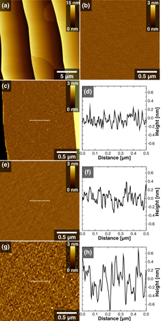
Figure 1. AFM surface images of (a), (b) a BL-covered SiC(0001), and MBE-grown graphene films prepared at a substrate temperature of 950 °C for growth times of (c) 60 min, (e) 120 min and (g) 240 min. The respective line section analysis corresponding to the white dashed lines are shown in (d), (f) and (h).
Download figure:
Standard image High-resolution imageRaman measurements performed on the center of the surface terraces, for samples grown at a temperature of 950 °C and Δt between 30 and 240 min, are displayed in figure 2(a). The displayed spectra correspond to what is obtained after subtracting the SiC- and BL-related background signals from the raw data. They show the typical graphene-related Raman features, namely the defect-induced D- and D'- lines at ∼1380 and ∼1610 cm−1, the normal E2g mode (aka G-line) at ∼1590 cm−1, the double-resonant two-dimensional (2D)-line at ∼2720 cm−1, and the second order line D + D' at ∼2970 cm−1 [27]. Note that measurements performed at several surface terraces yielded very similar results, which show that the MBE-grown layers cover the whole substrate surface and not only isolated areas.
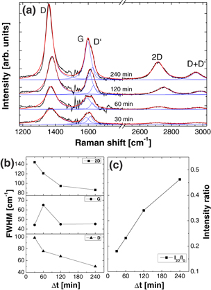
Figure 2. (a) Raman spectra and best fitting curves (the blue ones are single Lorentzians; the red ones are the sum of them) of samples prepared at TS = 950 °C with growth times as indicated in the plot. The spectra background originated from SiC, as well as that from the BL were removed. The spectra are shifted along the vertical axis for better visibility. (b) FWHM of the D-, G- and 2D lines as a function of growth time. (c) Ratio between the intensities of the 2D- and G-lines as a function of growth time.
Download figure:
Standard image High-resolution imageIt is observed that, by increasing growth time, the intensity of the graphene signal increases while the peak widths decrease. Especially the double resonant 2D-peak becomes clearly visible for growth times over 120 min. The full widths at half maximum (FWHM) obtained from the fittings of the D, G and 2D peaks, are presented, figure 2(b). Overall, the widths decrease monotonically with growth time, corresponding to an increase in structural order of the grown graphene [28]. Only the G-line FWHM of the layer grown for 30 min, appears as an exception. This might be due to the fact that the surface coverage for this film is very low (less than 0.4 monolayers (ML)—see XPS results below). Consequently, the Raman signal intensity is also very low, which may result in a non-ideal subtraction of the SiC- and BL-related backgrounds. In figure 2(c), the intensity ratio (I2D/IG) between the 2D- and the G-line versus growth time is displayed. It increases monotonically, confirming that the fraction of sp2-bonded carbon atoms arranged in the graphene honeycomb lattice increases with growth time [28].
Nevertheless, in spite of the observed improvement, the general features of the Raman spectra, in particular the appearance of an intense D peak, reveal that the MBE-grown graphene possesses a nanocrystalline and partially defective structure. Additionally, the existence point-like defects (see discussion regarding DFT calculations), such as mono- and divacancies, is a source of the high intensity of the D peak. This structural nature hinders the possibility of observing subtle changes in the Raman peaks, such as the expected broadening of the 2D peak as the graphene layer thickens with growth time (see XPS results next). For instance, the FWHM of the 2D peaks (the best value is ∼85 cm−1—see figure 2(b)) is still much larger than the typical values observed for mono- and bi-layer graphene on SiC(0001) prepared by surface graphitization (∼ 35 and ∼55 cm−1, respectively) [31]. Moreover, the nanocrystallinity of the films is probably the main reason associated with the increased surface roughness after MBE growth (see figure 1). It is plausible to assume that defective regions between the graphene domains (i.e. the grain boundaries) will be responsible for an increase of the rms roughness. Besides, neighboring graphene domains might be slightly tilted in respect to each other, which would generate additional surface corrugation and thus increase the final rms roughness. Finally, we have calculated the average lateral size (La) of the graphene domains by taking into account the width of the Raman peaks [29]. For the present case, La increases from ∼5–7 nm for Δt = 30 min to ∼15–20 nm for Δt = 240 min. These values can be taken as a lower limit for the actual crystallite sizes, since the model provided by Cançado et al [29] consider as defects only domain boundaries and not point-like defects (such as vacancies) located within the graphene domains. For a more detailed discussion see [13, 30].
XPS measurements were performed in order to determine the number of graphene layers grown by MBE as well as their bonding features. A representative measurement of the C1 s core level spectrum is presented in figure 3 for the graphene film grown on the BL/SiC(0001) template for 60 min. Two components of the spectrum are related to the BL (S1 at ∼284.70 eV and S2 at ∼285.35 eV). The lower energy component S1 is due to the covalent bonding between the BL and the SiC, while S2 arises due to the sp2-bonded carbon within the BL [23]. This shows that the BL remains unaltered during MBE growth even for the longest employed growth time, as also observed by Raman spectroscopy (not shown). It also reveals the absence of strong interaction (i.e. via covalent bonding) between the BL and the uppermost MBE-grown graphene. The component corresponding to the SiC bulk is seen at ∼283.61 eV, while the one at ∼284.61 eV is due to carbon in the sp2 bonding configuration forming the MBE-graphene. From the intensity ratio between the SiC and graphene components (taking into account the existence of the BL as well), the thickness of the MBE films could be deduced. It monotonically increases from ∼0.4 ML for Δt = 60 min to 1.5 ML for Δt = 240 min. Hence, more than 120 min are needed to form one complete ML. The increase in thickness to 1.5 ML is likely an additional reason, besides nanocrystallinity, for the relatively large rms roughness of the layer grown for Δt = 240 min (see figure 1). Since this value corresponds to an average obtained for a large surface area, it is very likely that the AFM tip probes regions which locally contain a different number of graphene layers. This idea is corroborated by the fact that lower rms roughnesses were measured for thinner films, i.e. prepared with shorter growth times. Finally, it is observed that the graphene peak in the C1 s spectrum is shifted to higher binding energies with respect to the neutral position (284.45 eV). This means that the layer is n-type doped, similar to what is measured for monolayer graphene produced by surface graphitization on SiC(0001) [31]. However, the shift of ∼0.15 eV observed in the present case is smaller than the values observed for those samples (∼ 0.3 eV), indicating a reduced amount of intrinsic doping in the MBE-grown graphene.
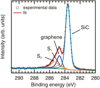
Figure 3. C1 s core level spectrum of a MBE grown graphene film on a BL/SiC(0001) template. Δt is 60 min in this case. There are two contributions related to the BL (S1 and S2), a third one related to the SiC bulk, and a fourth one related to the MBE-grown graphene layer.
Download figure:
Standard image High-resolution imageGID measurements were performed in order to obtain information about the structure as well as epitaxial orientation of the MBE-grown layers. The GID measurements were performed for the clean 'BL' substrate phase as well as for the sample after Δt = 240 min, where it is certain (as determined by XPS) that at least one full graphene monolayer has formed. Using this technique, the angle of x-ray incidence (0.15°) is slightly smaller than the critical angle of total reflection (0.21°). In that case GID may serve as an extremely surface sensitive tool, since the x-ray wave-field decays exponentially within the sample [32]. This enables investigations on mono- and few-layer graphene films. With GID, the lattice planes orthogonal to the sample surface are analyzed by diffraction and information about in-plane lattice parameters and the in-plane orientation can be obtained. By rotating the sample with respect to the incident beam, a so-called angular scan is performed. This scan provides a curved line qa in reciprocal space where every point on the curve has the same distance to the origin (00.0). By varying the azimuthal angle of detection and rotating the sample in a 2:1 ratio, we obtain a radial scan along qr, which corresponds to the length of the scattering vector (see figure 4(b)). In our experiment we measured reciprocal space maps (RSM) by a combination of angular and radial scans.
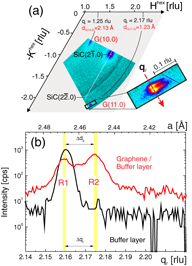
Figure 4. (a) Reciprocal space map of MBE-grown nanocrystalline graphene on a BL/SiC(0001) template. The inset shows a higher resolution map around the graphene (11.0) reflection, revealing a splitting into a BL and a graphene reflection. (b) Radial scan along the graphene (11.0) direction. The red curve shows a measurement on MBE grown graphene, the black curve presents an according scan on a bare BL sample. The peak positions of the BL (R1) and graphene (R2) reflections are indicated by the shaded area. The slightly lower peak intensity and enhanced background level of the curve measured for the MBE-grown graphene can both be attributed to its larger surface roughness in comparison to that of the pristine BL/SiC(0001) sample.
Download figure:
Standard image High-resolution imageThis is presented in figure 4(a). The axes are scaled to the reciprocal lattice units of the SiC substrate. The reflections associated with SiC, BL and graphene appear at the same angular positions, revealing that the graphene film and the BL are in-plane aligned with the substrate. In addition, the domains possess the same orientation, since a distribution of many randomly oriented domains would lead to a diffraction ring at the same radial position in reciprocal space. This result is the opposite of what has been measured for nanocrystalline graphene grown by MBE (using cracked ethanol as a C precursor) on epitaxial graphene on SiC [14]. In that work, samples analyzed by reflection high energy electron diffraction appeared to indicate that the graphene domains formed after MBE growth are not aligned to the underlying epitaxial graphene and SiC substrate. The present GID result also contradicts the notion that graphene synthesized by MBE should generally be composed of nanocrystals that are randomly aligned compared to the substrate [12, 15]. Apart from the different experimental procedures (e.g. solid-source versus gas-source MBE), one can speculate about the fundamental difference observed between the present results and the ones from [14] by simply considering the fact that the BL/SiC(0001) and the epitaxial graphene/BL/SiC(0001) are in fact very different substrates. An enhanced reactivity of the BL in comparison with epitaxial graphene will surely influence the C surface diffusion as well as the initial nucleation and growth of the graphene islands, even if the epitaxial process undergoes via vdW forces. In that respect, epitaxial graphene may act as a screening layer, suppressing effects associated with the underlying SiC. More investigations aiming at a complete understanding of the fundamental growth aspects are in progress.
Additionally, the GID measurements provided information about the lateral size of the graphene domains. By fitting the graphene-related R2 peak (see figure 4(b)) with a Gaussian function, a lower limit for the domain size could be estimated via the application of the determined fitting values into the Scherrer equation. The value is 35 nm, which agrees well with that derived from the Raman data. In order to examine a larger angular range we performed line scans with an azimuthal sample rotation of 130° (not shown here). Therein, only graphene (and BL) peaks with a separation of 60° emerge with an intensity that is two orders of magnitude higher than the background signal. The fact that the graphene films possess only one crystallographic orientation raises questions about the limited size of the domains (limited to a few tens of nm). In fact, the scan in angular direction over the graphene peak reveals a FWHM of ∼0.5%, revealing hence a narrow distribution in the rotational alignment. This might already be enough to hinder coalescence of neighbor islands. Furthermore, due to the relatively low growth temperatures (950 °C), an ineffective healing of defects in the grain boundary regions, which possibly contain even localized amorphous structures, may also be a factor impeding coalescence.
The inset in figure 4(a) shows the RSM with higher resolution around the graphene (11.0) reflection. A splitting in two components can be observed. One of the two reflections corresponds to graphene and one to the BL. In figure 4(b) a line scan in radial direction over the split peak is shown. For comparative purposes a scan of a bare BL/SiC sample is also added therein. By comparing these two scans the R1 peak can unambiguously be attributed to the underlying BL. The graphene reflection (labeled R2 in figure 4(b)) is clearly shifted toward higher qr in comparison to the BL reflection, which stands for a smaller lattice parameter in the analyzed in-plane direction. The lattice parameters derived from figure 4(b) are 2.450 and 2.468 Å for the MBE-grown graphene and the BL, respectively. This yields a relative mismatch of ∼0.7%. Interestingly, the lattice parameter of the MBE-grown graphene is about 0.45% smaller in comparison to the standard lattice parameter of graphite (2.461 Å) [33].
There are several potential reasons that could cause such a contraction, among them: (i) the contraction could be related to the different linear thermal expansion coefficients of graphene and SiC [34, 35]. Based on this difference, Ferralis et al [34] estimated that a compressive strain in graphene of up to ∼0.8% can arise upon sample cooling down to room temperature, since SiC contracts during cooling while graphene expands. (ii) The strong corrugation of the BL, product of its partial covalent bonding to the SiC [22], could contribute to the apparent contraction of the (2D projected) lattice parameter of the uppermost nanocrystalline graphene, despite the existent epitaxial relation between them. Indeed, recent first-principles calculations [9] quantify this corrugation of epitaxial monolayer graphene films on the BL to be approximately 0.4 Å (top to bottom atom in a graphene plane commensurate with a (6√3 × 6√3)R30° mesh of the SiC substrate below). (iii) A lateral contraction of graphene could also occur due to the intrinsic presence of defects and domain boundaries in the nanocrystalline film. In fact, the strong D peak in the Raman signal for Δt = 240 min as well as the small-scale structures seen in the AFM image (see figure 1(d)) would all allow for the presence of zero- or one-dimensional defects in the films. We estimate the graphene film contraction that would result from specific defect types and densities by DFT below.
Regarding point (i), strain up to 0.4% has been inferred by Raman spectroscopy for epitaxial monolayer graphene grown by surface thermal decomposition on SiC(0001) [36]. A similar contraction was directly linked to substrate thermal contraction in a recent study of near-perfect CVD-grown graphene on Ir(111) [33]. However, the contraction observed by us extends to a smaller lattice parameter than that found in [33, 36]. In a perfect graphene plane, we would expect the contraction observed by us to induce the formation of wrinkles/nanofins for strain relief, but we observe no such wrinkles in our graphene films, according to AFM analysis.
To estimate the possible contributions of (ii) and (iii), we performed DFT calculations of isolated graphene sheets. The calculations were performed using the all-electron, localized basis set code FHI-aims ('tight' settings) [37] and the Perdew–Burke–Ernzerhof (PBE) functional [38] with a correction for vdW effects, PBE + vdW [39]. At this level of theory, the lattice parameter of a perfect, infinite periodic flat graphene sheet is a = 2.463 Å. The calculated value for monolayer graphene on SiC is practically the same (within 0.1%). We note that, while we include the vdW correction for consistency with earlier work [9], it has no strong effect on the in-plane lattice parameters of interest here. Even when just using only the PBE functional, a = 2.467 Å for a perfect graphene sheet. Beyond the original vdW correction of Tkatchenko and Scheffler [39], the strength of effective interatomic C6 coefficients that describe the vdW interaction in carbon-based nanostructures may vary considerably with the structure [40] and could significantly change out-of plane interactions with a graphene sheet. However, their effect will still be small on the energy scale of interest for the in-plane lattice parameter, which is dominated by the covalent interactions that are described by the PBE functional itself.
To estimate the influence of the possible substrate-induced corrugation (point (ii) above), we proceed as follows. We take the fully relaxed structure of a graphene sheet with a (13 × 13) supercell situated on top of the 'BL', as determined in [9]; its calculated maximal corrugation perpendicular to the surface (top to bottom atom) amounts to 0.41 Å. The MBE-grown graphene on the BL should show the same approximate corrugation. If this corrugation led to significant stress in the plane, a perfect graphene sheet with the same (fixed) z corrugation should experience the same stress and should thus contract. In fact, however, relaxing all in-plane coordinates and lattice parameters of such a graphene plane with fixed z corrugation leads to a surface area that corresponds to an effective graphene lattice parameter of a = 2.462 Å, i.e. the calculated contraction is less than 0.05%.
Finally, we address the potential impact of different types of defects on the in-plane lattice parameter. Coming to one dimensional defect types (domain boundaries) first, figure 5 shows the development of the effective lattice parameter of finite-size graphene flakes as a function of flake size. The effective lattice parameter is calculated by fully relaxing the flat graphene flakes, then taking the average of all C–C nearest-neighbor bond distances in the flake and converting this value to the equivalent lattice parameter of a perfect honeycomb mesh. Two different types of flakes are considered, i.e. those with a H-saturated boundary and those with no capping atoms at the boundary. A significant contraction of the effective lattice parameter results in either case. To approach the GID-observed lattice parameter of 2.450 Å (figure 4) by this effect alone, the equivalent saturated flakes would have to be extremely small (less than 0.8 nm in diameter). The equivalent unsaturated flakes, however, could be significantly larger: about 2 nm even if they were perfect otherwise. With increasing flake size, the net contraction decreases rapidly for larger sizes.
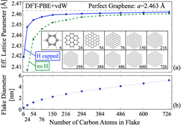
Figure 5. (a) Calculated (DFT-PBE + vdW) effective lattice parameter (average C–C bond length) in a series of fully relaxed graphene flakes of finite size with (squares) and without (circles) hydrogen termination at the edges. The hydrogen-terminated flakes are shown in the inset. The lattice parameter of a flat, strain-free, periodic graphene sheet calculated in DFT-PBE + vdW is indicated by a dashed line. (b) Diameter (maximum C–C distance) of the flakes used in (a).
Download figure:
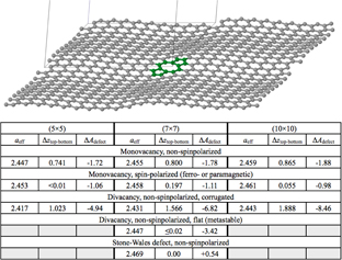
Standard image High-resolution imageLocalized zero-dimensional (point-like) defects can also lead to strain and corrugation in graphene sheets [41, 42]. Figure 6 gives quantitative predictions for the strain, corrugation and net area change of a periodic graphene sheet (all calculations: DFT-PBE + vdW, reciprocal sampling equivalent to 20 × 20 or denser with respect to the primitive unit cell, residual forces and stresses below 0.001 eV Å−1 after complete, stress-tensor based relaxation of 2D unit cells, and 50 Å vacuum thickness between graphene sheets in z direction) with well-defined arrays of specific common defect types: monovacancies, divacancies and the Stone–Wales defect (for a recent review, consider, e.g. [41]).
Figure 6. Top: calculated fully relaxed (atomic positions and unit cell) structure of a graphene sheet with a (10 × 10) periodic arrangement of 5-8-5 divacancy defects (atoms highlighted in green). The in-plane supercell and surface normal are indicated by thin lines. Bottom: DFT-PBE + vdW calculated effective lateral lattice parameter aeff (in Å), the top-to-bottom corrugation Δztop-bottom (in Å) and effective area lost (gained) per defect, ΔAdefect (in Å2) of different defect types and periodicities in an ideal, free-standing graphene sheet.
Download figure:
Standard image High-resolution image
Monovacancies are perhaps the most studied point defect type in graphene (e.g. [42–44] and many references therein). In particular, the relation between theoretically imposed isotropic strain and monovacancy properties such as corrugation and spin polarization has been the subject of a recent, exhaustive study [42]. We here consider only the fully relaxed, stress-free local optimum structures as calculated by DFT-PBE + vdW. Figure 6 shows that monovacancies would be associated with significant strain and corrugations of perfect graphene sheets if no spin polarization were included. However, monovacancies are in fact paramagnetic defects that carry a significant local moment in DFT-PBE + vdW. This leads to a slight reduction of the compressive strain compared to a perfect graphene sheet, and thus also to a reduction of the overall distortion (buckling of the monovacancy and corrugation of the sheet). Even with 2% monovacancies (modeled by a (5 × 5) periodicity in figure 6), monovacancies alone would not yet lead to the full strain seen in the GID experiments above.
Among the other possible point defect types in graphene, divacancies are in fact thermodynamically more stable than monovacancies [41, 45], a tendency that is even enhanced by compressive strain [46]. The calculated results for divacancies with corrugation shown in figure 6 were obtained by starting from the fully relaxed, non-spinpolarized monovacancy geometries and removing the most strongly buckled atom (in z direction) in the monovacancy. As can be seen in the table and the structure of the (10 × 10) divacancy defect in figure 6, this procedure leads to very significant strains and buckling in a free-standing graphene sheet. The sheet curvatures seen at the defect locations follow the trend described in the literature [41]. It is also obvious that such defects could easily explain the GID-observed lateral lattice parameter reduction even for relatively low defect concentrations ((10 × 10) case). In fact, significant corrugations of this kind are seen in atomically resolved STM images of defects generated in HOPG by ion implantation (e.g. figure 1 in [47]). However, even if a divacancy were completely flat, the associated strain would still be significant. For comparison, figure 6 also includes the case of a flat, (7 × 7) periodic divacancy, which is a local structure optimum about 0.1 eV higher in energy than the corrugated divacancy arrangement. Even at this defect density, divacancies would be sufficient to explain the observed strain. Finally, we also include the case of the Stone–Wales defect, which results from the rotation of a single C–C bond, but the number of C atoms remains unchanged. Here, a slight expansion, not compression, of the overall lattice parameter would result.
Idealized theoretical defects and boundaries are certainly just approximations to the experimental reality of MBE-grown nanocrystalline graphene films such as those seen in the AFM image of figure 1(d). If defects left over from the growth process really do play a role, the morphology of such films would likely be characterized by a combination of the defect types considered here, as well as others. It thus seems qualitatively plausible that the strain induced by defects may indeed significantly contribute to the overall lattice parameter contraction that we observe in GID. Eliminating the potential for metastable defects will be important to achieve large-scale homogeneous electronic properties of epitaxially MBE-grown sheets. On the other hand, controlling the nature and concentration of defects in a graphene sheet during growth may be a promising path toward strain-engineered graphene films.
4. Conclusions
Nanocrystalline graphene layers synthesized by MBE on (6√3 × 6√3)R30°-reconstructed SiC surfaces were investigated. Raman spectroscopy measurements indicate an improvement in the structural quality with increasing growth time. The average size of the graphene domains exceeds 15 nm for layers grown for 240 min. The (6√3 × 6√3)R30° BL persists throughout the growth process as confirmed by XPS measurements, which also reveals that the upper-most MBE-grown graphene layers consist of sp2-bonded carbon and thus seems to weakly interact with the underlying BL-covered substrate. Strikingly, GID measurements reveal that the graphene domains are in-plane aligned to the underlying template and have the same orientation. Therefore, despite its nanocrystalline nature, the layer possesses an epitaxial relation to the substrate. In addition, GID also shows that the lattice parameter is strongly contracted. By a first-principles approach for isolated graphene sheets, we derive reference values for the lattice parameter contraction expected from (i) a possible substrate-induced buckling, (ii) the edges associated with finite carbon flakes (hydrogen-saturated or unsaturated) and (iii) monovacancies, divacancies and Stone–Wales defects in periodic supercell arrangements in hypothetical, infinite-periodic graphene sheets. The calculations demonstrate that a lattice parameter contraction will arise from all defects except for the Stone–Wales defect. The largest contraction is associated with the divacancy, which also induces a significant buckling in free-standing graphene sheets. A low concentration of defects is thus one possible explanation for the observed contraction.
Finally, the present results also demonstrate the feasibility of using MBE as an alternative method for the controlled synthesis of graphene layers directly on an insulating substrate. Nevertheless, it is also clear that the growth conditions (e.g. substrate temperature) have to be optimized in order to allow the preparation of layers with higher structural quality, i.e. domains exceeding hundreds of nanometers in size and lower defect concentration.
Acknowledgments
The authors thank K Biermann for the critical reading of the manuscript; H-P Schönherr, M Höricke and C Herrmann for technical support. The authors thank the ESRF for providing beamtime during project SI-2449 and Roberto Nervo for his support during the experiment. This work was supported by the European Union within the project ConceptGraphene (grant number 257829).