
Abstract
Properties of superconducting nanowires set the performance level for superconducting nanowire single photon detectors (SNSPDs). Reset time in commonly employed large area SNSPDs, 1–10 ns, is known to be limited by the nanowire's kinetic inductance to the load impedance ratio. On the other hand, reduction of the kinetic inductance in small area (waveguide integrated) SNSPDs prevents biasing them close to the critical current due to latching into a permanent resistive state. In order to reduce the reset time in SNSPDs, superconducting nanowires with both low kinetic inductance and fast electron energy relaxation are required. In this paper, we report on a study of kinetic inductance in narrow (15–100 nm) and long (up to 120 μm) superconducting MgB2 nanowires made from 5 nm thick films, offering such combination of properties. Such films were grown using hybrid physical chemical vapor deposition, resulting in a critical temperature of ∼32 K, and a switch current density of 5 × 10⁷ A cm−2 (at 4.8 K). Using microwave reflectometry, we measured a kinetic inductance of Lk0(4.8 K) = 1.3–1.6 pH/□ regardless of the nanowire width, which results in a magnetic field penetration depth of ∼90 nm. These values are very close to those in pristine MgB2. We showed that after excitations by a 50 fs pulsed laser the reset time in 35 nm × 120 μm MgB2 nanowires is 130 ps, which is more than a factor of 10 shorter than in NbN nanowires of similar length-to-width ratios. Depending on the bias current, such MgB2 nanowires function as single-, double, or triple-photon detectors for both visible (λ = 630 nm) and infrared (λ = 1550 nm) photons, with a dark count rate of <10 cps. Although the apparent photon detection efficiency seems so far to be low, further technological advances (uniform nanowire width, smaller thickness, increasing the switching current closer to the pair-breaking current) may improve this figure of merit.
Export citation and abstract BibTeX RIS

Original content from this work may be used under the terms of the Creative Commons Attribution 4.0 license. Any further distribution of this work must maintain attribution to the author(s) and the title of the work, journal citation and DOI.
1. Introduction
During the last two decades we have seen enormous progress with superconducting nanowire single photon detectors (SNSPDs), from first demonstration of principles [1] to integrated circuits and a wide range of applications in nanophysics [2], high speed communication [3], quantum information [4], quantum key distribution [5], laser-ranging [6], deep space communication [7], etc. SNSPD's operation is based on photon assisted disruption of supercurrent in a superconducting nanowire, which is dc-biased close to the critical current [8, 9]. Because the superconducting energy gap Δ is in the meV-range, a large number of non-equilibrium quasiparticles are generated at visible or infrared photon (∼eV) impacts. Both the small width of the nanowire, w and the critical current, Ic being close to the pair-breaking current ensure high detection efficiency [10, 11]. After hot-spot formation, the bias current is diverted from the SNSPD into the readout. Within a relaxation time, τ0 (set by electron-phonon non-elastic scattering and phonon escape into the substrate), non-equilibrium quasiparticles recombine into Cooper pairs. Until the supercurrent in the nanowire is restored and the hot-spot disappears (the reset time), SNSPD is blind to any further incoming photons. NbN SNSPDs, being the first one where single-photon sensitivity was demonstrated, still provide the shortest reset time for a given detector area, compared to SNSPDs made from other superconductors. In 5 nm thick NbN films, the quasiparticle relaxation time τ0 is ∼30–50 ps [12, 13]. However, in long (l) and narrow (w) NbN nanowires, large kinetic inductivity (Lk0(4.8 K) = 80–90 pH/□) (inductance per square of the nanowire, l= w) leads to a significantly slower current return (restoration of the superconducting state), resulting in a much larger reset time τ [14]: τ= Lk/RL ≫ τ0, where Lk = Lk0× l/w is the total kinetic inductance of the nanowire and RL is the impedance of the read-out circuit (∼50 Ω). This is particularly critical in large area SNSPDs, with a kinetic inductance as large as hundreds of nH, leading to a reset time of a few tens of ns. On the other hand, large kinetic inductance delays current return from the load RL back into the SNSPD, prior to the hot-spot cooling down, hence preventing the SNSPD from latching into a permanent normal (non-sensitive) state [15]. To a certain extent, the reset time can be reduced by choosing a high-impedance load. However, much increased RL leads to a reduction of the maximum non-latching bias currents, hence precluding SNSPDs from reaching high detection efficiencies [16]. This problem is particularly pronounced in short SNSPD, where shunting resistors of small values or extra inductors in series are required to avoid latching, which does not altogether allow reaching short reset times [17, 18].
Apart from low-Tc superconductors (NbN, Nb, NbTiN, TaN, MoN, WSi, MoSi, etc) [10, 15, 19–21], magnesium diboride (MgB2) nanowires have also shown ability for single photon detection in both visible [22] and IR [23] ranges. However, the reset time in those MgB2 SNSPDs was reported to be 2–3 ns, i.e. close to that for NbN SNSPDs, the fact that was left unexplained. Previously it has been shown that in clean MgB2 (attainable in 50–200 nm thick films) the magnetic field penetration depth λ0 is at least an order of magnitude shorter than that in NbN [24], which should lead to a small kinetic inductivity (Lk0= μ0 λ0 2/d). Apparently, due to a large number of defects in the abovementioned thin MgB2 films (normal state resistivity ρn> 300 μΩ × cm) kinetic inductance increases, which affects the reset time. Recently, we managed to deposit 5 nm thick MgB2 films with a critical temperature >30 K and ρn comparable to that in thick films. Furthermore, in such thin films, a quasiparticle relaxation time is measured to be τ0= 12 ps [25], and which all together suggests that MgB2 nanowires might provide a solution for high speed photo detection.
In this work, we study both kinetic inductance and response rate in nanowires, with a large variation of width (15–900 nm) and length (3–120 μm), made from clean (low normal state resistivity) and ultra-thin (5 nm) MgB2 films. Observing a kinetic inductance as low as 1.5 pH/□, we show experimentally that a 130 ps voltage relaxation time can be achieved in 120 μm- long devices into a standard 50 Ω readout circuit with a 100 MHz repetition rate. When biased close to the critical (switch) current, such devices show a linear dependence of the number of response pulses vs the incident laser power, corresponding to the single-photon detection regime.
2. Film deposition and device fabrication
MgB2 films were grown on 6 H-SiC substrates using a custom-built hybrid physical chemical vapor deposition (HPCVD) system [26, 27]. The system was designed for a low deposition rate (∼2.5–3 nm min−1) with a diborane gas flow of 2 sscm (5% B2H6 in H2) and a deposition temperature of 700 °C. As a result, continuous MgB2 films could be routinely obtained as thin as 5 nm, as shown by transmission electron microscopy (TEM) (figure 1(a)), with a critical temperature of 32–34 K (figure 2(a)). Film growth on the SiC substrate is epitaxial, which ensures that bulk properties of MgB2 are preserved in the thin films as manifested in a fairly low normal-state (residual) resistivity of ρn= 10–15 µΩ × cm, a high switch current density of Jc∼ 5 × 10⁷ A cm−2, and a small magnetic field penetration depth of λ= 90 nm (see further in the text). TEM analysis was conducted on a set of MgB2 films of varying thickness, where the thickness proportionality to both the diborane flow and the deposition time was verified.
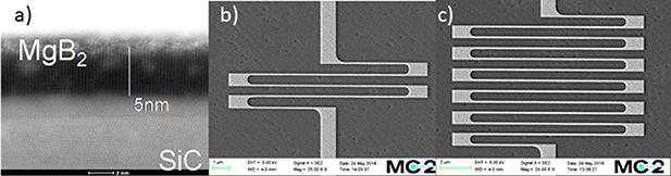
Figure 1. (a) TEM image of a 5 nm- thick MgB2 film on the SiC substrate. (b), (c) SEM images of a meandering MgB2 nanowires. Scale bars are given in each of the images.
Download figure:
Standard image High-resolution image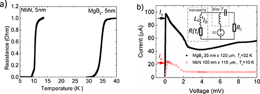
Figure 2. (a) Superconducting transitions (normalized resistance) in an MgB2 and an NbN nanowire. (b) I(V)-curves (at 5 K) for a MgB2 and a NbN nanowire, utilized for the response rate experiments (see figure 5). Bias points are indicated with arrows. The inset shows simplified schematics of a photon detector (a variable resistance and an inductor, representing kinetic inductance in the nanowire) with a biasing network and a readout load (e.g. a low-noise amplifier).
Download figure:
Standard image High-resolution imageSubsequently, MgB2 films were transferred (vacuum broken) into a dc-magnetron sputtering system where plasma assisted cleaning of the film surface was done followed by in situ sputtering of a 20 nm thick Au film. This was followed by the device fabrication route #1 which starts with defining the coplanar waveguide (CPW) contact pads and alignment marks on the MgB2 films with a 20 nm gold layer. A layer of polymethyl methacrylate (PMMA—70 nm) on top of copolymer (MMA—470 nm) was utilized as a positive tone bilayer resist system for electron beam lithography. The subsequent development in isopropanol/water mixture (10:1), electron beam physical vapor deposition of Ti–Au–Ti (10 nm–200 nm–40 nm), and lift-off in acetone leaves the desired patterns on the substrate. The first 10 nm titanium layer promotes the adhesion of Au whereas the final 40 nm layer serves as a mask for gold contact pads later on during the Ar+ ion milling. The nanowire patterns were defined via another electron beam lithography step with a negative tone resist (ma-N 2401—100 nm), developed in tetramethlyamonium hydroxide aqueous solution (ma-D 525) followed by rinse in DI water. The remaining MgB2 and the initial 20 nm Au layer, except on top the nanowire, were etched using Ar+ ion milling. Finally, the negative resist mask layer was removed with acetone and the initial 20 nm Au layer on top of the nanowire was removed by another Ar+ ion-milling step (figures 1(b) and (c)).
A second fabrication route has also been explored which differs from the route #1 by absence of the initial gold protection layer (20 nm Au in Route #1) on top of the MgB2 film. In this case, the final ion milling step, as in the case of route #1, is unnecessary, therefore there is no need in removing the negative resist mask and hence Au layer. The route #2 contains fewer steps, whereas we have not observed any MgB2 film degradation due to absence of the protective Au layer.
In order to compare both the kinetic inductance and the reset time to those in a well-established material system, we have also fabricated and tested 100 nm wide NbN nanowires, both 115 μm and 460 μm long. The NbN film (d∼ 5 nm thick, as estimated from the deposition rate) was deposited by DC reactive magnetron sputtering in an Ar + N2 environment on a 330 µm thick C-plane double side polished sapphire substrate maintained at 800 °C. The film was patterned into 100 nm wide (100 nm spacing) meandering nanowires with reactive ion etching (CF4:O2, 5:1 flow ratio) through a mask defined by e-beam lithography on a positive (PMMA—80 nm) resist. During the RIE process, the total pressure was kept as low as possible (3.8 mTorr being the lowest used to provide a stable plasma discharge) in order to increase the etching anisotropy. Electrical contact pads (as single-port 50 Ω CPW) were fabricated in 10 nm Ti/200 nm Au/40 nm Ti using a standard lift-off process. The NbN film between the CPW contacts was removed by means of wet-etching (nitric acid/hydrofluoric acid/acetic acid, 5:3:3) with a resistive mask placed over the nanowires (photo resist AZ1512). The critical temperature was ∼10 K and the room temperature sheet resistance was ∼300 Ω/□, which corresponded fairly well to NbN film characteristics for previously published NbN SNSPDs.
3. Experimental techniques
All experiments were conducted in a cryogen-free probe station Lakeshore CRX-4K (base temperature 4.8 K) with an optical view port and microwave ground-signal-ground probes on XYZ manipulator stages (figure 3(a)). Kinetic inductance was obtained from the imaginary part of the microwave impedance (Z(f) = 2π × f × Lk, where f is the probing microwave frequency), which was measured using a (10 MHz–67 GHz) Vector Network Analyzer Rohde&Schwarz ZVA 67. The vector network analyzer (VNA) calibration was done using a wafer with calibration standards (matched (50 Ω), open, and short) placed on the same cooling stage next to the MgB2 samples. Therefore, both the VNA calibration and impedance measurements of MgB2 nanowires were performed in a single cool-down. Magnetic (or geometric) inductance in superconducting films as thin as those utilized in our experiments is negligibly low, and it can be calculated analytically using the approach from [28] as a function of the film thickness d and the temperature T:
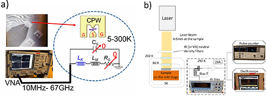
Figure 3. (a) The kinetic inductance measurements set-up. Chip layout (right), samples on the 5 K stage in the cryo-probe station with the microwave probe contacted (the view through the pressure window and the IR filter) (left-top), the VNA (left-bottom). (b) The optical characterization set-up. The laser flood illuminates the sample on the 5 K cooling stage through the window in the cryo probe-station.
Download figure:
Standard image High-resolution imagewhere μ0 is the vacuum permeability and λ0(T) is the magnetic field penetration depth. Considering the d = 5 nm and λ0(5 K) = 90 nm,  (5 nm, 5 K) = 0.5 fH/□.
Lasers flood-illuminated the samples through a quartz pressure window of the probe station. The standard IR filter (not transparent for 1560 nm photons) on the 60 K shield was replaced with a WG12012-C window (Thorlabs). The output beam from the cw λ = 630 nm laser diode module required no extra collimation, resulting in a light spot diameter of 3–4 mm. The IR (λ = 1560 nm, Toptica FemtoFErb 1560, 100 MHz repetition rate) 50 fs pulse laser is fiber-coupled and a fiber launcher was utilized to collimate the IR laser beam. The IR-laser spot size (on the sample) was approximately 5 mm, verified using SNSPD photo counts vs the laser XY-shift. Two sets of light attenuators were utilized for the visible and IR light. The emission of both lasers (∼2 mW and ∼100 mW (average) for the λ = 630 nm and λ = 1560 nm lasers, respectively) was attenuated to a level where suppression of the switch current in the nanowires is not visible anymore.
At room temperature, both microwave readout and dc biasing were arranged (figure 3(b)) though a bias-T (Picosecond 5547, 12 kHz–15 GHz) followed by a low noise amplifier (MITEQ 3D-0010025, 0.5–5 GHz) and either a real time oscilloscope (Keysight Infiniium 54854 DSO, 4 GHz, 20 GSa s−1) or a pulse counter (HP 53131A 225). Nanowires were biased with a Yokogawa 7651 programmable dc source.
4. Kinetic inductance
As measured in a large variety of samples (width, length and fabrication batches), the kinetic inductivity in thin MgB2 nanowires was 1.35–1.60 pH/□ at 4.8 K (figure 4(a)). In the case of defect-free uniform films, the total kinetic inductance  is expected to be proportional to the length-to-width ratio (l/w) and hence to the total resistance R in the normal state (40 K).
  is the MgB2 film sheet resistance in the normal state. This trend was indeed observed (figure 4(b)), which confirms scalability of thin-film transport properties from the micron- to the nano-scales.

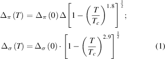
Figure 4. (a) Kinetic inductivity (at 4.8 K) for samples with various widths and lengths. (b) The total kinetic inductance (at 4.8 K) vs the normal state resistance R(40 K) for the same samples as in (a). (c) Kinetic inductivity vs temperature for nanowires from two batches with critical temperatures of 35 K and 32.7 K. The fits are made using equation (2), where energy gaps for both π- and σ-bands were calculated using equation (1) and the experimental Tc.
Download figure:
Standard image High-resolution imageKinetic inductance (and its temperature dependence) is a sensitive indicator for superfluid (Cooper pairs) density, hence providing the value for the superconducting energy gap. In MgB2, π- and σ-sheets of the Fermi surface display quite dissimilar energy gaps  and
and  , with temperature dependences following [29]:
 and
and  are zero temperature energy gaps in π- and σ-sheets.
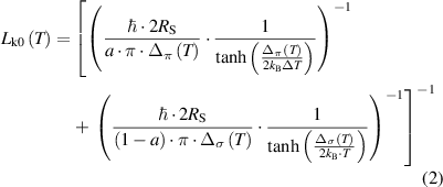
Previously, in the frame of double-band modeling [30], it has been shown that electrodynamic properties in MgB2 can be analyzed by considering two quasi-layers (electrons of both π- and σ-bands) in parallel, with a finite (yet, weak) interband scattering. In particular, partial contribution from each band to both the condensate energy and the superfluid density varies according to temperature and magnetic field, e.g. at zero magnetic field, the π-band is expected to contribute about a> 70% to the superfluid density (∝1/λ0 2) at T< (Tc—2 K). The exact value of the coefficient a depends on the interband scattering rate, and has to be evaluated for each particular case. However, the general trend seems to be correct, as in [24], where it was shown that λ0 vs the mean free path can be modelled considering predominantly the π-band. In [31], a satisfactory agreement with experimental λ0 (T) was demonstrated for thick films, considering two bands with an assumed π-band weighing coefficient a = 0.8. For a general case of two conduction bands, the kinetic inductivity can be calculated from the imaginary part of the BCS conductivity [32] as:
 is the Boltzmann constant, and
  is the 2π-normalized Planck constant.
By fitting equation (2) to the experimental Lk0(T) data (figure 4(c)), we obtained the superconductor energy gaps at T= 0. Our results showed that equation (1) holds even for extremely thin MgB2 films considering that  and
and  , with an interband coefficient a =0.85. For a mean experimental value of Lk0(5 K) = 1.5 pH/□, we can obtain the effective magnetic field penetration depth: λ0 (5 K) = (Lk0 × d/μ0)1/2 = 90 nm. This value for the penetration depth for the measured resistivity of ρn= 10–15 µΩ × cm fits well with the λ0 (ρn)-dependence previously reported for thick MgB2 films [24]. Increase of the penetration depth is related to a shorter electron mean free path
  vs the BCS coherence length
  as
as  , where
  is the penetration depth in the clean limit [32]. The BCS coherence length can be estimated from ξ0
π
= ħvF/(πΔπ
) = 66 nm, considering the a–b plane averaged Fermi velocity as vF ∼ 5.4 × 10⁵ m s−1 [30]. For ultrathin films, as utilized in our study, electron scattering on the film surface might become significant (i.e.
is the penetration depth in the clean limit [32]. The BCS coherence length can be estimated from ξ0
π
= ħvF/(πΔπ
) = 66 nm, considering the a–b plane averaged Fermi velocity as vF ∼ 5.4 × 10⁵ m s−1 [30]. For ultrathin films, as utilized in our study, electron scattering on the film surface might become significant (i.e.  5 nm), hence increasing both the residual resistivity and the penetration depth.
Small kinetic inductance in MgB2 nanowires is a very attractive feature in SNSPD applications. For one of the longest (in the number of squares, i.e. the L/w ratio) of the utilized in our study MgB2 samples (35 nm × 120 μm, 3428 squares) we measured its impulse response on excitations from a 50 fs pulsed laser (λ= 1550 nm). The measured total inductance for this sample was 5100 pH, which is expected to result in a voltage fall time of τ = Lk /RL = 102 ps for a 50 Ω readout. The measured voltage impulses corresponded to the 100 MHz repetition rate of the laser. The rise and the fall time of the nanowire response were 90 ps and 130 ps (10%–90%), respectively (figures 5(a) and (b)). The observed fall time is close to that calculated from the kinetic inductance.
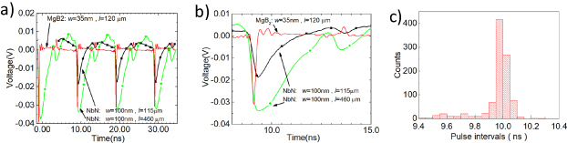
Figure 5. (a), (b) Voltage response to the IR pulsed laser (50 fs, 1560 nm, 100 MHz repetition rate) of a MgB2 (35 nm × 120 μm (thin red, Lk = 5 nH) sample and two NbN samples (100 nm × 115 μm (squares, Lk = 54 nH) and 100 nm × 460 μm (circles, Lk = 200 nH)) detectors with a total kinetic inductances (width and length variation). The same readout chain was used for all detectors (0.05–5 GHz LNA + 4 GHz oscilloscope). (c) Statistics for the response intervals (time span of 10 μs) for the MgB2 nanowire as in (a).
Download figure:
Standard image High-resolution imageFor comparison, both the kinetic inductance and the impulse response were measured for two types of 100 nm wide NbN nanowires, 115 μm (1150 squares) and 460 μm (4600 squares) long. The kinetic inductance was measured in these samples (54 nH and 200 nH, respectively) using the same method as for MgB2 samples, corresponding to an average Lk0(5 K) = 45 pH/□. This value is ∼½ of the previously reported [14], which can be due to variations of the NbN film quality (choice of the substrate, deposition conditions, etc), due to uncertainty in the film thickness, as well as due to variations of Lk measurements techniques. The voltage impulse decay time in NbN nanowires was 4.1 ns for the 460 μm long sample and 1.3 ns for the 115 μm long sample (figures 5(a) and (b)), both corresponding well to the measured kinetic inductance.
As follows from figures 5(a) and (b), MgB2 nanowires demonstrate a reset time (10%–90%), which is at least a factor of 10 faster than in NbN nanowires of a similar geometry. Despite of being biased at the switch current, MgB2 nanowires with a kinetic inductance of 5 nH demonstrate no latching, which follows from the fast decaying voltage impulses (figures 5(a) and (b)). Fast quasiparticles relaxation (12 ps in MgB2 vs 50 ps in NbN) [25] is a positive factor which reduces the effect of latching in small kinetic inductance samples.
The voltage impulse rise dynamics in superconducting nanowire detectors has previously been studied both experimentally and theoretically in SNSPDs made from NbN [14, 33, 34]. One of the conclusions made there was that the rise time is proportional to the square root ratio of the total inductance and the normal domain resistance  , approaching nearly linear dependence at high inductance values
  . Because the sheet resistance in NbN is of the order of 500 Ω, the rise time in NbN SNSPDs is much less than the fall time. The sheet resistance in thin MgB2 films is 20–30 Ω, which can lead to a rise time longer than in NbN for the same total inductance. Considering that in MgB2 the kinetic inductance is a factor of 30–60 lower than in NbN, the increased rise time will be noticed only for very long samples. Detailed modeling and experimental studies are needed in order to clear the question of hot-spot formation in MgB2 nanowires and to understand what will be the limiting factor for the rise time both for short and long samples.
For an initial estimate of the MgB2 photon detector response jitter, we utilized statistics for response pulse intervals collected within a 10 μs time-slot through a single oscilloscope scan, which was triggered by the first detection event. The response interval jitter is still ∼50 ps, which corresponds to a ∼25 ps jitter of the rising edge (figure 5(c)). This value is an upper limit for MgB2 nanowire detectors, because a jitter less than that in NbN could be expected in MgB2 considering a factor of 33 lower kinetic inductance [33].
5. IR- and visible light detection
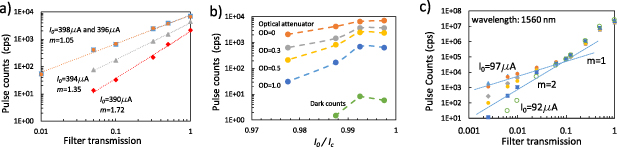
Direct demonstration of single photon detection capability requires a 100% photon coupling and a known quantum efficiency. Considering that the former is a challenging engineering task and the latter would require complex modelling, the single photon detection mode is often verified by statistical analysis of the pulse counts per photon flux [1] or inter-counts intervals [11]. We chose the first method, utilizing initially a cw laser (630 nm). The photon count rate N vs the laser attenuation F is shown in figure 6(a) at several bias currents for a 90 nm wide and 40 µm long nanowire. For bias currents I0 ⩾ 396 µA, the pulse count is linearly proportional to the photon flux, N ∝ F. For smaller bias currents we observed that N ∝ Fm
, where m> 1, which indicates that multi-photon detection mode becomes dominant. These results show that, in contrast to NbN nanowire detectors, the single photon detection mode is limited in MgB2 nanowires to a narrow bias current range in the vicinity of Ic (figure 6(b)). Physical modeling using accurate material parameters is required in order to obtain a full understanding of photon detection in MgB2 thin film nanowires. In this moment, we note that the aforementioned fact is probably caused by a smaller size of the normal domain  (compared to the nanowire width), formed by the photon-deposited energy. Its order of magnitude could be estimated using an expression
  for a photon energy
  [9]. The total density of electronic states N(0) at the Fermi level in MgB2 can be obtained e.g. from the electron specific heat data as
  , where
  is the electron specific heat coefficient in the normal state [29],
  is the mass density, and M =45.9 g mol−1 is the molar mass. The obtained N(0) is close to that in NbN [35], whereas Tc in MgB2 is a factor of 3 higher. Therefore, a higher dc current (vs Ic) is required to extend the normal domain to the edges of the nanowire. The fact that we have not observed any rise of the kinetic inductance at bias current close to the switch current most probably indicates that the switching current in our MgB2 nanowires is constriction-limited [36]. The observed dark count rate in the studied MgB2 nanowire detectors was very small, <10 cps at the highest utilized bias current (398 µA), despite the fact that the samples were not shielded from either the electrical or magnetic field interference. At such bias current the dark count rates in NbN SNSPDs often reach values of >103–105 cps [34, 35]. It is another indication that the switch current in our samples is limited by a constriction in a short section on the nanowire, leaving the most of the nanowire under-biased.
Figure 6. (a) Pulse counts vs relative photon flux (filter transmission with different optical densities OD). The MgB2 detector (90 nm × 40 μm, Ic= 399 μA) was illuminated with a cw laser (630 nm). Lines are N ∝ Fm fits. (b) Pulse counts vs normalized bias current, for the same sample and the laser as in (a); (c)) Pulse counts vs photon flux for a 35 nm wide and 120 μm long nanowire (Ic= 97 μA) illuminated with a pulsed laser (50 fs, 1560 nm). Lines are N ∝ Fm fits. All measurements were made at 4.8 K.
Download figure:
Standard image High-resolution image
Similar results were obtained for detection of IR photons (λ= 1560 nm) from the 50 fs pulsed laser by a 35 nm × 120 μm MgB2 sample (Ic= 97 μA). For I0 > 0.97 × Ic, a linear N(F) dependence (figure 6(c)) indicates that the detector response is triggered by single photon absorption events. For I0 < 0.97 × Ic, a combination of both one- and two-photon responses was observed (N ∝ Fm, m > 1). At a high photon flux (F > 0.1), i.e. at a large number of photons per pulse, multi-photon response even dominates at the highest bias current, as has been observed in NbN SNSPDs [37] for large laser power.
6. Conclusions
In our study, we investigated ultra-thin MgB2 films in an attempt to create a new material basis for SNSPDs. Previously published works have demonstrated that single photon sensitivity is achievable with MgB2 nanowires. However, the reported reset times were >1 ns even for relatively short devices, which we interpret to result from a high degree of disorder in those films, manifested in both high normal state resistivity and high kinetic inductance. HPCVD was known to be a way of making clean MgB2 films, which so far been limited to thicknesses >10–15 nm. MgB2 films thinner than that were reported to break into a set of isolated islands (Volmer–Weber growth mode). Using our custom-built HPCVD system we have previously observed that by reducing the deposition rate to its lowest limit (2.5–3 nm min−1) MgB2 films as thin as 5 nm can be deposited, which allowed to fabricate 1 μm2 devices (hot-electron bolometer, HEB, terahertz mixers) with a high switch current density. In the current paper, we show that even nanowires as narrow as 20 nm and with a large aspect ratio (L/w> 3000) can be fabricated using e-beam lithography and Ar+-ion milling using such MgB2 films. The obtained kinetic inductance is ∼Lk0(4.8 K) = 1.3–1.6 pH/□ corresponding to a magnetic field penetration depth of λ0 = 90 nm. Scalability of both the kinetic inductance and the normal-state resistivity from micrometer down to nanometer device scale indicates a high film uniformity. High quality of films is also manifested in a high critical temperature (>30 K), and a high switch current density (∼5 × 10⁷ A cm−2), approaching some of the highest values ever achieved in MgB2 films. With the reset time being limited by kinetic inductance, MgB2 nanowire detectors are expected to operate a factor of Lk0(NbN)/Lk0(MgB2)= 30–60 times faster compared to NbN devices. We confirm it experimentally by observing a voltage impulse decay time of 130 ps for an MgB2nanowire with a total kinetic inductance of 5 nH, whereas this figure is ∼4 ns for an NbN nanowire with a similar L/w ratio. Obtained results show that MgB2 nanowires are capable of single photon detection in both visible and communication (1.5 μm) spectral ranges, combined with a low dark count rate, hence forming a technological platform for sensitive and high speed single photon detectors with a large cross-section and a low jitter. It also becomes apparent that the observed switching currents are probably limited by constrictions (a local narrowing), which prevents devices to be biased at high enough currents, hence reaching high detection efficiencies. This issues could be resolved by optimization of the nanowire fabrication process. At present conditions, considering the photon flux on the detector area, we estimate the detection efficiency as ∼10−2 %.
With the presently utilized deposition rate, the observed normal state resistivity in MgB2 films increases sharply whereas the critical temperature drops down as the film becomes thinner than 5 nm. Nevertheless, it appears to be interesting to investigate if further reduction of the deposition rate would result in even thinner films (2–3 nm) with the desired degree of uniformity, low kinetic inductance, and high switch current density. Further steps shall also be taken towards increasing nanowire uniformity, i.e. avoiding constrictions and hence increasing the current density in the biased nanowire. We consider it important in order to reach a high quantum efficiency in SNSPDs made from MgB2 films.
Acknowledgments
The authors would like to thank: Dr Olof Bäcke for conducting TEM analysis of MgB2 samples; Professors X X Xi and K Chen for sharing their experience with the HPCVD process for MgB2 films and enlightening discussions; and Usman Ul-Haq for the help with process development. MgB2 film technology was developed under an ERC grant 308130-Teramix. This research was also supported by Swedish Research Council (Grant Nos. 2016-04189 and 2019-04345) and by Swedish National Space Agency (Grant No. 198/16). Devices were fabricated in the Nanofabrication Laboratory of Chalmers University of Technology.