
Abstract
The paper presents the problem of design and simulation of a high-speed wide-band high-resolution analog-to-digital (ADC) converter working in a bandpass scenario. Such converters play a crucial role in software-defined radio and in cognitive radio technology. One way to circumvent the limits of today’s ADC technologies is to split the analog input signal into multiple components and then sample them with ADCs in parallel. The two main split approaches, time interleaved and frequency splitting, can be modeled using a filter bank paradigm, where each of these two architectures requires a specific analysis for its design. In this research, the frequency splitting approach was implemented with the use of a hybrid filter bank ADC, which requires an output digital filter bank perfectly matched to the input analog filter bank. To achieve this end, an analog transfer function, together with an assumption of strictly band-limited input signal, has been used to design the digital filter bank so far. In contrast, the author proposes dropping the band-limit assumption and shows that the out-of-band input signal has to be taken into account when designing a hybrid filter bank.
1 Introduction
In the last few decades, analog-to-digital converter (ADC) architectures based on parallel sampling [2] have received a strong interest. As a result, we have two parallel architectures, the time interleaved (TI) [20] and the hybrid filter bank (HFB) [10, 14, 19], which appear to be able to overcome the technological bottleneck of wideband sampling with high resolution. However, these architectures are sensitive to imperfections and require calibration to reach better performance [1, 5, 7–9]. Digitally assisted architecture used for calibration purposes offers promising prospects as the relative cost of energy consumed by digital electronic parts has been falling about ten times as fast as the cost of energy used by analog parts over the recent years [13].
The HFB ADC relies on sub-band sampling [2] and may be perceived as being derived from the perfect reconstruction (PR) digital filter bank [15, 17]. At the input of an HFB ADC, an analog filter bank (AFB) splits analog signal in frequency into an arbitrary number of sub-bands. Then, each sub-band is sampled critically, i.e., with a frequency twice as high as its bandwidth, and digitized by ADCs. In the third step, the outputs of each ADC are up-sampled to a Nyquist sampling frequency, which is twice as high as the bandwidth of the input analog signal. Eventually, all the signals are recombined by a digital filter bank (DFB) to form a stream of samples at the output of the HFB ADC. HFB architecture is similar to TI architecture except the input and output filter banks. Instead of using an AFB, the sample/hold time instant in each ADC is slightly shifted by the Nyquist sampling period. This process can be modeled with a time delay filter bank. Thus, the synthesis filter bank has simple aligning architecture. The concept of the TI ADC is easy to handle, but it has difficulty in compensating many types of distortions, which is due to the lack of a synthesis filter bank [3, 5, 20].
To the best of our knowledge, the existing approaches to the HFB make the assumption that the input signal is strictly limited to the band of interest [1, 7, 9, 16]. Thus, the sampled signal may only suffer from in-band aliasing distortions. This is indeed a strong assumption, which may appear too optimistic for the scenario in which many wireless channels dedicated to communication may be crowded. This remains true even if we consider the shape of the bandpass filter of the receiver. Therefore, it is important to figure out the impact of out-of-band energy aliasing on the performance of the HFB ADC.
The main contribution of this paper is threefold. Firstly, an in-depth analysis of HFB ADC architecture, which is essential for the understanding and designing of an HFB ADC, will be presented. The proposed methodology utilizes the frequency domain. A shifted Fourier transform is proposed to solve the problem with singularities of computations at frequencies \(0\) and \(\pi \). Secondly, an equivalent digital (ED) filter approach will be proposed to overcome the traditional assumption that the input signal is strictly band-limited, which is unrealistic in the case of telecommunication signals. Thirdly, an analysis of the impact of quantization effect on the overall HFB ADC system will be provided. A similar analysis can be found in [11], but our paper proves that the same result could be achieved while using the proposed ED filter bank.
The paper is organized as follows. Section 2 is a general introduction to parallel architectures of ADCs. Section 3 discusses bandpass sampling methodology and its consequences. Section 4 provides a detailed analysis of using HFB architecture for designing a bandpass ADC. In Sect. 5, an equivalent digital filter bank approach is proposed. In Sect. 6, a modification of the regular Fourier transform is introduced. Section 7 provides an analysis of the impact of quantization effect on the overall error in HFB ADCs. Section 8 deliberates results obtained from Matlab simulations.
2 HFB Architecture
HFB ADC architecture [1, 7, 9] is presented in Fig. 1. An input signal goes through an analysis filter bank \(H_m(s)\), where the signal is divided into \(M\) sub-bands. Hereafter, the signals in the channels are sampled, and then, after the up-sampling procedure, they go through a digital synthesis filter bank. The sum of all \(M\) channel signals compose a digital signal \(\hat{X}(z)\).

General architecture of hybrid filter bank ADC
The main advantage of this ADC architecture is that the ADCs used in sub-channels run at frequency \(D \le M\) times lower than needed for an input analog signal. Furthermore, the dynamic range of the signal at each ADC input is reduced because of analog filtering. Both facts allow more relaxed requirements for each ADC. If the number of channels \(M\) equals the down-sampling coefficient, then such a case is referred to as a critically (or maximally) sampled HFB, but a down-sampling coefficient \(D\) lower than \(M\) is also possible. In this case, one obtains a so-called non-critically sampled HFB—more details can be found in Sect. 4.1.
The analog filters chosen to build an analysis bank play the key role in HFB performance. Sub-band signal sampling will create aliasing in each sub-band coming from the stop-band attenuation of the adjacent channels. Ideally, this aliasing may be canceled when the digital filters of the synthesis bank are perfectly matched to the actual AFB. It has been shown that HFB ADCs may be very sensitive to mismatches that could arise from the tolerance of the analog components forming the analysis bank [7, 9]. This topic, however, is beyond the scope of this paper.
3 Bandpass Sampling
A possibility of using an HFB ADC to sample bandpass signal directly in intermediate frequency (IF) or radio frequency (RF) is worth consideration. According to Fig. 2, careful selection of sampling frequency \(f_e\) lets the signal be sampled and down-converted to the baseband in one step. This property of the HFB ADC can be very useful in software-defined radio and cognitive radio applications.

The effect of using different sampling frequencies in-band sampling techniques
To avoid aliasing, the input signal should be limited to band \(B = f_2 - f_1\) and the sampling frequency should satisfy the Nyquist principle \(f_e \ge 2B \). The sampling frequency can be analytically computed thanks to the formula proposed by Lyons [12] and Vaughan in [18]:
where \(f_c=(f_2-f_1)/2\) is the center frequency of the bandpass signal and \(m\) is an arbitrary positive integer. Lyons has proved that for an odd \(m\), spectral inversion property appears in bandpass signal after the sampling process and thus choosing an even \(m\) is more convenient.
In practice, all the above conditions are satisfied when a multiple of sampling frequency \(k f_e\) goes below \(f_1\) together with \(k f_e + f_e/2\) going above \(f_2\). This case is equivalent to \(m=2k\). A graphical representation of this situation is shown in the top plot in Fig. 2. The case when \(k f_e < f_1\) is shown in the middle plot and the case when \(kf_e +f_e/2 > f_2\) is presented in the bottom plot of Fig. 2. In these cases, one can observe aliasing in low- or high-frequency regions, respectively.
4 Analysis of HFB ADC
Let us consider a real-valued analog signal \( X(f) \) having a spectrum of interest limited to:
but not necessarily zero elsewhere, with \(f\) being the continuous frequency ranging from \(-\infty \) to \(\infty \) in (Hz). Such a signal can be sampled using Nyquist sampling frequency \(f_e\), where \(f_e \ge 2|f_2-f_1|\).
Let \(H_m(f)\) be the transfer function of the m-th filter from an AFB (Fig. 1). Then, the output of this channel will be:
The AFB splits the band of interest \(B\) into \(M\) uniform sub-bands. Each sub-band signal is then sampled using sampling frequency \(f_e/M\). The spectrum at the output of each ADC is given by:
where \(T_e=1/f_e\) is the sampling period. Next, the signals are up-sampled by factor \(M\):
Note that \(S_m(f)\) is a periodic function with period \(f_e/M\).
Continuing, the output of the HFB can be described as follows:
Using (3), the above equation can be rewritten as:
All the above equations are defined in a continuous frequency domain, so the spectra of signals \(Y_m(f)\), \(S_m(f)\), \(\widehat{X}(f)\) are continuous in frequency, but one thing should be pointed out. The sampling process is modeled by the multiplication of the original signal by a comb function (i.e., periodic Dirac impulses). Therefore, the signal spectrum exhibits periodicity, i.e., \(\widehat{X}(f)\) is periodic with period \(f_e/M\). However, because of the design assumptions, the expected period should be \(f_e\), which is a multiple of the real period. Thus, without losing generality, the spectrum region \(f\in (-f_e/2,f_e/2)\) can be chosen for further deliberations.
The next observation is that the output of an HFB is described completely by the sampled signal, so a continuous frequency domain can be replaced with a discrete frequency domain. It is noteworthy that signals flowing through HFB branches are in fact digital (i.e., discrete in time and in values) after sampling. Accordingly, we introduce the normalized angular frequency:
Consequently \(\omega \in (-\pi ,\pi ) \). Additionally, while using the normalized angular frequency, the following notation is introduced:
Note that without losing generality, it can be assumed that \(f_e=2\pi \) . Then, the Eq. (7) can be rewritten as:
where an imaginary value \(j\) is added to point out that all spectra in general have imaginary values.
4.1 Non-critically Sampled Configuration of HFB
In this paper, the overall structure of the HFB is considered, with the sampling frequency \(D\) times lower than the Nyquist frequency (see Fig. 1). Thus, the subsampling coefficient \(D \in [1,\dots ,M] \) makes it possible to choose between multirate configurations of the HFB [17]. For \(D=1\), one can obtain a so-called single rate (SR) configuration, in which all ADCs use the Nyquist sampling frequency. For \(D=M\), one can obtain a so-called critically sampled (CS) configuration, in which the sampling frequency is critically low if we take into consideration the frequency band of analysis filters. For the remaining values of \(D\), a non-critically sampled configuration is inferred. Nevertheless, in all the cases, analysis filters \(H_m(j\omega )\) split the input signal spectrum into \(M\) equal sub-bands, since the HFB utilizes \(M\) filters. Therefore, equation (10) can be rewritten as:
4.2 Strictly Band-Limited Input Signal
Let us now consider a signal of a strictly bandpass character:
so the infinite sum in Eq. (7) becomes finite because:
for \(l \notin (kf_e,(k+1)f_e)\), where \(k=f_1/f_e\). Accordingly, there exist only \(D\) nonzero shifted frequency terms \(X(j\omega _D^{(l)})\). Therefore, in this case, Eq. (11) can be rewritten as:
This expression corresponds to the classical formula found in [1, 7, 9], which reflects the strictly band-limited constraint.
Let us reformulate Eq. (14) as:
where
defines the distortion transfer function, and
defines the aliasing transfer function.
The HFB system defined by Eq. (15) has the perfect reconstruction property if:
which means that the system distortion function should be a pure delay function and all the aliasing terms should equal zero. Equivalently, these conditions can be rewritten in a matrix form as:
where \({\mathbf {F}}(j\omega )=[ F_0(j\omega ), F_1(j\omega ),\dots , F_{M-1}(j\omega ) ]^T\) is the vector of frequency responses of synthesis filters, \({\mathbf {H}}(j\omega )\) is the matrix of AFB’s modulated frequency responses:
and \(\bar{{\mathbf {T}}}(j\omega )\) is the vector of frequency responses for the distortion and aliasing transfer functions:
The frequency responses of a synthesis filter bank can then be calculated by solving linear Eq. (19) for \({\mathbf {F}}(j\omega )\).
4.3 Non-Band-Limited Input Signal
If the input signal does not completely meet the bandpass assumption (12), one should take into account all the aliasing terms from Eq. (11) so the output signal becomes:
In this expression, the system distortion function remains the same as in Eq. (15), but there is now an infinite number of aliasing terms and thus an infinite number of linear equations.
5 Equivalent Digital Analysis Filter Bank
This section introduces the equivalent digital (ED) AFB that allows handling the “Non-Band-Limited Scenario” with a finite number of linear equations like in Eq. (22).
An ED AFB is depicted in Fig. 3 and is defined as follows: The impulse response of the digital system \(G_m(e^{j\omega })\) is the sampled response of the continuous filter \(H_m(f)\) excited by signal \(X(f)\), where \(X(f)\) has a constant power spectral density in band \(B\) and not necessarily \(0\) elsewhere. The sampling rate is \(f_e\), and the normalized angular frequency is \(\omega =2\pi f/f_e\). Therefore, the ED transfer function \(G_m(e^{j\omega })\) depends not only on the analog analysis filters but also on the out-of-band input signal. The spectral shape of this signal does not affect the approach as long as good approximation of it is available.

One channel of equivalent digital AFB
Note that the notation \(e^{j\omega }\) is used instead of \(j\omega \) to emphasize the fact that the discrete Fourier transform (DFT) is used in the development of the HFB instead of the continuous Fourier transform used in Eq. (19).
Using an ED filter bank, the output of the system can be defined as:
where
is a distortion transfer function, and
are aliasing transfer functions. Comparing (15) or (22) to Eq. (23), one can be surprised by a lack of the input signal but when an ED AFB is used, function \(G_m \left( j \omega _{D}^{(l)}\right) \) contains both in-band and out-of-band input signals together with AFB transfer functions.
Applying the PR property, formula (19) can be rewritten using an ED AFB:
where matrix \({\mathbf {G}}(e^{j\omega })\) elements are modulated transfer functions of the ED AFB, similar to matrix \({\mathbf {H}}(j\omega )\).
It is very important to make sure that in the proposed approach one obtains a finite number of linear equations, regardless of the signal’s band assumption. In this approach, the ED filter bank \({\mathbf {G}}(e^{j\omega })\) combines information on the transfer function of the analog filter bank \({\mathbf {H}}(j\omega )\) as well as on the in-band and out-of-band input signal \(X(j\omega )\). Matrix \({\mathbf {G}} (e^{j \omega } ) \) equals \({\mathbf {H}} (j \omega ) \) (for a set of discrete angular frequencies \(\omega \) chosen in the Fourier transform) if and only if the assumption of a strictly limited band is satisfied for the input signal—see Eq. (12). If not, then \({\mathbf {G}} (e^{j \omega }) \ne {\mathbf {H}} (j \omega ) \) since the digital equivalent filter bank has to involve out-of-band aliasing information.
6 Frequency Modeling of Bandpass Sampling and Bandpass Filter Bank
To design an HFB ADC, an ED filter bank has to be calculated through the sampling response of the analysis filter bank:
Using a subsampling scheme and choosing the Nyquist sampling frequency:
one can obtain:
If we consider a strictly band-limited input signal, then the above sum has only two nonzero terms for \(l=\pm n\), so
Arguments can be found in [18], proving that the best choice of sampling frequency is when there is “no signal” at \(f_1\) and \(f_2\)—i.e., the power of the signal equals zero at these frequencies. It is equivalent to the modified subsampling Nyquist condition:
and it results in:
Therefore, when Eq. (30) is calculated using a regular DFT, the discrete frequencies are:
Thus, one can obtain
As a consequence of the modified Nyquist condition (31), the system \({\mathbf {G}}_m(e^{j\omega })\) has no constraints for \(\omega =-\pi \) and \(\omega =0\) (i.e., \(k=[-N/2,\;0]\)). Since the input signal has no energy at these frequencies, the shape of \({\mathbf {G}}_m(e^{j\omega })\) could be set freely for \(\omega =-\pi \) and \(\omega =0\). A straightforward solution that satisfies the Hermitian symmetry of the spectrum for real signals is to replace the null values of \( G_m(e^{j0})\) and \( G_m(e^{-j\pi })\) by ones that are interpolated by using tools like complex spline functions. In that case, the bandpass filters at the edges of the band of the input signal after sampling will, respectively, become low-pass and high-pass filters in baseband.
These problematic calculations were performed twice: first during the HFB ADC design, when matrix \({\mathbf {G}}(e^{j\omega })\) had to be calculated, and then during the simulation, when the sampling process was producing branch signals \(Y_m(e^{j\omega /D})\). In both cases, continuous signals were sampled, which caused the down-conversion of these signals to frequency interval \(\omega \in (-\pi /D,\pi /D)\). Moreover, in both cases, real-valued signals (in time domain) were expected, so the spectrum should exhibit the Hermitian symmetry property.
Therefore, the authors propose another approach to choosing a set of frequencies:
The regular Fourier transform is replaced by a shifted one defined by:
It is easy to check that functions \(e^{-j\pi n (2k+1)/N}\) span the frequency space like in the case of the regular DFT. Thus, our approach produces an orthonormal transform. The only difference is that the proposed transform is calculated at frequency points shifted by half of the frequency bin.
7 Modeling of Quantization Errors in HFB ADC
Let us assume that an HFB ADC is designed to satisfy the PR condition and the system is simulated with the use of floating point arithmetic. Then, the main source of output noise is the quantization error caused by ADCs in every branch of the HFB ADC. It is noteworthy that as long as we use identical ADCs, the power of the noise is the same in every branch.
The signal to quantization noise ratio (SQNR) is defined as follows:
where \(\sigma _x^2\) is the variance of the input signal and \(\sigma _e^2\) is the variance of quantization noise.
If a signal with a dynamic range of \([-{\varDelta }_x,{\varDelta }_x]\) is quantized by a b-bit uniform mid-tread quantizer [4], the quantization step is given by:
and the power of quantization noise under the assumption of uniformly distributed uncorrelated white noise is:
Consequently, after substituting \(\sigma _e^2\) to Eq. (38), one obtains:
The ratio \({\varDelta }_x/\sigma _x\) is called the overload factor (\(OF\)). Each kind of signals has its own \(OF\). For example, a full-scale sinusoidal signal has the standard deviation \(\sigma _x={\varDelta }_x/\sqrt{2}\). Therefore, \(OF\) equals \(\sqrt{2}\) and (41) becomes
Full-scale uniformly distributed noise has \(\sigma _x={\varDelta }_x/\sqrt{3}\), so \(\textit{OF}\) equals \(\sqrt{3}\) and
In the case of a Gaussian signal with an unbounded dynamic range, there are two noise sources: quantization and saturation noise. Increasing the \(OF\) allows minimizing the saturation probability, but it deteriorates the SQNR—see Eq. (41). In [6], the authors suggested a way to find an optimal \(OF\), which minimizes the overall noise caused by both types of errors. The usual choice for Gaussian signals is \(OF\in (3,4)\), but it is worth noting that the optimal \(OF\) depends on the number of bits. For instance, the optimal \(OF\) for \(b=16\) equals \(5.9\) [6].
Table 1 lists simulation results for a 16-bit ADC. \(R_e\) is the penalty term calculated from the \(OF\):
For a signal with a bounded dynamic range like sine or uniformly distributed signals, one may avoid saturation by the correct choice of the \(OF\), but an \(\textit{OF}\)-related drop in the SQNR cannot be avoided.
\(S_e\) denotes the saturation penalty term induced by saturation noise. It is calculated as the difference between the effective SQNR and the SQNR defined in Eq. (41), which does not take into account the saturation noise:
The third column of Table 1 represents the value of saturation probabilities for different \(OF\) values. A saturation probability is calculated according to:
where \({\text {erfc}}()\) is the complementary error function.
The second column of Table 1 represents SQNR values calculated with an assumption that the only existing effect is the \(\textit{OF}\), so it represents theoretically the best possible SQNR value. The last column represents SQNR values, which take into account both the \(\textit{OF}\) and saturation effects. Observing the second column, one can conclude that the bigger \(\textit{OF}\) is, the worse theoretical SQNR becomes. Nevertheless, if saturation effect is taken into account, the effective SQNR rises with the rise in \(\textit{OF}\). And finally, for the \(OF=5.9\) both SQNR values become more or less the same. For other than 16-bit ADCs, different optimal \(\textit{OF}\) values should be calculated.
7.1 The Overall Impact of Quantization Error
The impact of quantization error from every branch on the overall transfer function at the output of a HFB ADC was analyzed in [11]. However, what must be checked here is whether the ED filter bank approach causes any changes in the impact of quantization error. Let us assume a strictly band-limited input signal (see Eq. (12)) and an ideal analog filter bank with a passband gain equaling one. The word “ideal” means no ripples and no leakage between bands (see Fig. 8). Accordingly, by using the methodology proposed in this paper, one obtains an ideal synthesis filter bank, which means that all the aliasing terms are zeros—\(T_l(e^{j\omega })=0\). Therefore, the output signal should contain only the \(T_0(e^{j\omega })\) term, so any observed differences are caused by the effect of branch signal quantization. According to Eq. (23), we get:
where quantization error is the sum of branch quantization errors:
Note that a linear model of quantization effect has been assumed—see Fig. 4.

Model of quantization errors that are injected in each branch of ED AFB
Let us consider an input signal \(x(t)\) with a power equal \(\sigma _x^2\) and a dynamic range of \([-{\varDelta }_x,{\varDelta }_x]\). This signal is fed into an ideal analog filter bank, where each filter has an equivalent noise bandwidth equal to:
The signal power at the output of each filter equals \(\sigma _x^2/M\), so the dynamic range of the ADC and consequently the quantization step can be decreased by \(\sqrt{M}\). The quantization noise power in each branch becomes:
where \(Q\) is defined by Eq. (39) and \(Q_m\) is the quantization step of the ADCs in each branch.
Quantization errors are injected in every branch just before the synthesis filter bank—see Fig. 1. These errors are filtered out by the synthesis filter bank, and the overall power of quantization noise at the output can be found by:
Currently, two extreme cases have to be considered: a critically sampled (CS) configuration of the HFB and a single rate (SR) configuration of the HFB.
1) CS case: in a CS configuration (i.e., \(D=M\)), each filter in the synthesis filter bank has a gain of \(M\), and thus, its equivalent noise bandwidth becomes:
and consequently one obtains:
which is the same quantization error power as in the case of a single ADC. In other words, using a CS HFB ADC, we should not expect better bit resolution (i.e., a better SQNR) than for ADCs utilized in the HFB structure.
2) SR case: In a SR configuration (i.e., \(D=1\)), each filter in the synthesis filter bank has a unity gain, so its equivalent noise bandwidth equals:
Consequently, when using Eqs. (50) and (51), one obtains:
Therefore, the overall quantization error is \(M\)-times smaller than in the case of a single ADC (40). This is an important result, because at the cost of higher sampling frequency, one can expect better bit resolution. It means that utilizing branch ADCs, which have finite bit resolution, leads to a decrease in the final quantization error power, proportional to the number of channels. Therefore, the effective bit resolution increases.
8 Simulation Results
Let us define the experimental distortion function of the system as the ratio of the output to the input signal:
where \(X(j \omega )\) is the baseband equivalent spectrum of the continuous input signal perfectly confined to band \(B\) and down-converted to the baseband.
By combining Eqs. (56) and (15), the following formula can be obtained:
where the experimental aliasing of the system can be calculated as:
Let us define ED transfer functions \(\bar{G}_m(e^{j\omega })\) calculated for each simulation. These transfer functions may differ from the respective functions \(G_m(e^{j\omega })\) used while designing the HFB, as the out-of-band signal is not necessarily the same.
The theoretical distortion function can be inferred from Eq. (26):
where \(\bar{\mathbf {G}}^{(0)} (e^{j\omega })\) is the first row of the matrix \(\bar{\mathbf {G}}(e^{j\omega })\). Similarly, the aliasing function can be calculated:
It should be noted that as long as the input signal satisfies the assumption used to design the synthesis filter bank, matrix \( {\mathbf {G}} (e^{j\omega })\) equals matrix \( \bar{\mathbf {G}}(e^{j\omega })\), so the PR condition can be reached.
8.1 Results of HFB ADC Simulations in Frequency Domain
In our tests, the AFB was composed of eight sixth-order bandpass Butterworth filters. The In-band to the Out-band signal Power Ratio (IOPR) is defined as the power ratio of the input test signal in the band of interest (normalized to \(1\)) to the out-of-band signal power.
Different scenarios for the HFB ADC system were considered and tested by simulation. The setup of each test was composed of three steps:
-
1.
System design: In the first step, the transfer function \( {\mathbf {G}} (e^{j\omega )}\) of the ED analysis filter bank is derived from the assumed IOPR. Then, a synthesis filter bank \({\mathbf {F}}(e^{j\omega })\) is calculated by solving Eq. (26) with respect to \({\mathbf {F}}(e^{j\omega })\).
-
2.
System simulation: In the second step, the spectrum of test signal \(X(f)\) with a given IOPR (not necessarily the same as in the system design step) is generated and processed by the HFB ADC system designed in the previous step.
-
3.
Result checking: Eventually, experimental and theoretical distortion transfer functions and aliasing functions are calculated according to Eqs. (56), (58) and (59), respectively.
For the system design step, the bandwidth of the input signal was normalized to \(1[\pi \text{ rad/s }]\) and it lies in the following interval:
whereas the simulation was run considering the normalized frequency range \(\omega \in (-10,10)(\pi \text{ rad/s })\).
In the first scenario, an assumption was made that the input test signal is similar to the input signal presumed during the design stage (it means both signals have the same IOPR value and determined phase). In this case, the HFB ADC system utilizing the regular Fourier transform maintains very good performance for all frequencies except the spikes observed in both the distortion and the aliasing function. These spikes come from singularities of the matrix \({\mathbf {G}}(e^{j\omega })\) as stated in Sect. 6. Every row of this matrix is a modulated version of the ED AFB; thus, for an eight-channel HFB ADC, one can observe eight spikes—see Fig. 5. When a shifted Fourier transform is used, the problem of singularities is resolved, so in Fig. 6 one can observe nearly perfect performance of the HFB ADC system, i.e., very small ripples in the distortion function. Note that such small ripples in a (dB) scale mean that the transfer function of our system is very close to one for all frequencies. Also, aliasing is very small, below \(-250\) dB in the whole band. Based on this observation, a decision was made to perform all the consecutive simulations by using the proposed shifted Fourier transform.

Distortion functions and experimental aliasing function obtained using the regular Fourier transform. The HFB was designed for IOPR = 30 dB, while the test was performed for a signal with IOPR = 30 dB

Distortion functions and experimental aliasing function obtained using the proposed shifted Fourier transform. The HFB was designed and tested for IOPR = 30 dB
The next considered scenario was designing an HFB for a strictly band-limited signal (see Eq. (12)), which corresponds to IOPR = \(\infty \) and for a wideband input signal that in its turn corresponds to IOPR = \(0\) dB. In both cases, as long as the test signal was similar to the signal assumed during the design process, i.e., with the same IOPR with perfect phase recovery, the HFB system was able to reach nearly ideal performance: the distortion function \(T_x\approx 0\) dB and the aliasing function \(T_a<-250\) dB. In contrast, when the test input signal corresponds to the opposite scenario, i.e., the assumed IOPR = \(\infty \) whereas the test signal IOPR = 0 dB, the performance deteriorates dramatically: \(T_x\approx 2.7\) and \(T_a\approx -25\) dB, as shown in Fig. 7.

Comparison between several HFB designs (from \(\infty \) to 0 dB IOPR) for different input test signals characterized by various values of IOPR
To get more insight into the sensitivity of the HFB system when the input signal does not match the one assumed for the design, both HFB systems were simulated using test signals with different IOPRs: \(\infty \), 125, 100, 75, 50, 25, 10, 5, 2, 1, 0.1, 0.01 and 0 dB. The results are illustrated by Fig. 7. The plots demonstrate that for the design of an HFB system with IOPR = \(\infty \), both figures of merit (the distortion function and the aliasing function) decrease with a slow slope as a function of the IOPR of the input test signal. For the design of an HFB system with other IOPR values, the two figures of merit fall dramatically as soon as the test input signal deviates slightly from the design assumption. One can also see that the best performance is achieved when the input signal matches the assumption used for the design. Therefore, it is clear that the proposed methodology, which involves the IOPR, is suitable only if information about the out-of-band signal is effectively available with good approximation.
8.2 Impact of Quantization Effect
To check the quantization impact on an HFB ADC system quality, an ideal eight-channel AFB was used (see Fig. 8). Such a filter bank discards completely out-band and in-band aliasing, so all the distortions observed in the \(T_x(z)\) and \(T_a(z)\) functions are caused solely by the quantization errors injected by each ADC in the branches of the HFB structure. What is interesting, the proposed design algorithm is capable of finding an ideal SFB, which is demonstrated in Fig. 8. In this case, the test signal is a wideband signal of unknown phase, with constant power spectral density and IOPR = \(\infty \). In every branch, a 16-bit ADC is assumed; thus, the ADC’s output signal \(Y_m(e^{j\omega })\) is quantized accordingly. Two configurations were simulated:
-
SR with \(M=8\), \(D=1\),
Fig. 8 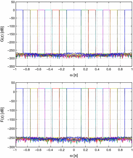
The transfer functions of an ideal eight-channel analysis (top) and synthesis (bottom) filter bank for a critically sampled configuration of HFB ADC
-
CS where \(M=D=8\).

Figure 9 displays the theoretical and experimental distortion transfer functions of the CS configuration of the HFB ADC system. The differences between the theoretical distortion transfer function (blue line) and the experimental distortion transfer function (green line) are caused by quantization and do not exceed the peak-to-peak value of 8e\(-\)4 dB, which corresponds to the spurious-free dynamic range (SFDR) of about \(-81\) dB. For the SR configuration of the HFB, the peak-to-peak ripples of the experimental distortion function do not exceed 4e\(-\)4 dB, which corresponds to the SFDR of about \(-87\) dB.

Distortion transfer function of an HFB ADC using 16-bit ADCs. The top plot shows result for a CS configuration with \(M=D=8\). The bottom plot shows result for a SR configuration with \(M=8, D=1\)
The spectrum of HFB ADC quantization errors is presented in Fig. 10. The green line (referred to as \(\text {SQNR}_\text {ADC}\)) displays the theoretical value of quantization error calculated according to Eq. (41) (for a traditional equivalent ADC), which, except for bit resolution of the ADC, also involves the overload factor of the test input signal. The red line (referred to as \(\text {SQNR}_\text {expr}\)) displays an experimentally obtained SQNR, calculated according to Eq. (38). In the upper plot of Fig. 10, corresponding to a CS configuration, the experimental SQNR is similar to the theoretical one—\(\text {SQNR}_\text {ADC} \approx \text {SQNR}_\text {expr}\), whereas in the lower plot, (\(\text {SQNR}_\text {ADC}\)—\(\text {SQNR}_\text {expr} \approx 8\)) dB. These results are consistent with our expectations (see Eq. (55) for the SR configuration of a HFB ADC and Eq. (53) for the CS configuration). Additionally, since an ideal AFB is used in these simulations, then \(\text {SQNR}_\text {expr}\) should be equal to the average quantization error \(Q_e(e^{j\omega })\), which is indicated by the blue dashed line. One can observe that in both CS and SR cases, \(Q_e(e^{j\omega })\) approximates \(\text {SQNR}_\text {expr}\).

SQNR function of an HFB ADC using 16-bit ADCs. The top plot shows the result for a CS configuration with \(M=D=8\). The bottom plot shows the result for a SR configuration with \(M=8, D=1\)
The consolidated results of a HFB ADC simulation for several numbers of bits are presented in Fig. 11. In the case of the CS configuration, the power of the HFB ADC quantization error \(\text {SQNR}_\text {expr}\) is approximately the same as the quantization error calculated for a traditional ADC. However, while observing the plot for the SR configuration, one can notice an improvement of about 9 dB. According to equation (55), the power of the quantization error for SR configuration should be \(M\)-times lower than for a traditional ADC, so for \(M=8\), it is exactly 9 dB.

Quantization error in the function of ADC’s number of bits. The top plot shows the result for a CS configuration where \(M=D=8\). The bottom plot shows the result obtained for a SR configuration where \(M=8, D=1\)
Figure 12 presents the results for a more realistic scenario. Instead of an ideal AFB, the filter bank composed of sixth-order Butterworth bandpass filters is used; 16-bit ADCs were utilized like in the previous case. The plots refer to the CS and the SR configurations, respectively. The IOPR for the design and simulation steps was set at \(\infty \). In both cases, similar results were obtained compared to the ideal AFB case—cf. Fig. 11.

The SQNR and quantization error function of an HFB ADC using sixth-order Butterworth analog filters and 16-bit ADCs. IOPR\(=\infty \), \(M=D=8\) (top plot), \(M=8, D=1\) (bottom plot)
In Fig. 13, all the plots refer to the situation when an HFB ADC was designed with an assumption that IOPR = \(\infty \), whereas it was set at IOPR = 30 dB during the simulation. In the top plot of Fig. 13, one can observe substantial fluctuations in quantization error in the function of frequency. In fact, these fluctuations are caused by out-of-band input signal as the system has not been designed to cancel it. As a consequence, the sum of distortions and quantization error effects can be observed.

The SQNR and quantization error function of an HFB ADC using sixth-order Butterworth analog filters and 16-bit ADCs. IOPR = 30 dB, \(M=D=8\) (top plot), \(M=8, D=4\) (middle plot), \(M=8, D=4\) (bottom plot)
It is noteworthy that quantization error is almost flat for all frequencies in the case of the SR configuration, cf. the middle plot of Fig. 13. Like in the previous case (top plot), the IOPR of the test signal was set at 30 dB, while the system was designed for the IOPR equaling \(\infty \). Nevertheless, the quantization error is almost flat because of the flatness of the transfer function, quite unlike in the top plot, where the sum of the distortion and quantization effect is visible. Moreover, in both cases the \(\text {SQNR}_\text {expr}\) (red line) is much lower (about \(-45\) dB) due to high aliasing caused by the power of out-of-band signal.
The simulation results presented in the bottom plot of Fig. 13, generated for a non-CS configuration (\(M=8,\;D=4\), while all the other conditions remained the same) look quite similar to those in the middle plot. Some bigger fluctuations caused by non-flat distortion function and quantization errors can be observed, cf. Eq. (47).
9 Conclusions and Further Work
The paper addresses modeling a bandpass ADC designed to sample wideband signals directly at RF or IF frequency. The proposed ADC utilizes HFB architecture. It presents the design and simulation methodology of a bandpass HFB ADC system in frequency domain.
An ED (equivalent digital) analysis filter bank (cf. Eq. (26)) is proposed to solve difficulties caused by wideband input signal, i.e., the bandwidth of the input signal is wider than the assumed band of interest. It has been shown that the overall transfer function of an HFB ADC system is sensitive not only to the imperfections of the analog filters used in the AFB but also to the out-of-band spectrum of the input signal. Taking into consideration the power of the spectrum outside the band of interest, the presented approach shows that it is possible to design a synthesis filter bank which suppresses not only in-band but also some out-of-band aliasing. This is the main contribution of the proposed approach compared to those published so far, which have been all based on the strict band limitation constraint. The author of this paper is aware of the fact that HFB ADC architecture is also sensitive to analog filter bank imperfections caused by the production process, temperature, aging, etc., but this issue is beyond the scope of this paper.
Two different methods of frequency-domain modeling of baseband aliasing caused by the sampling process have been proposed. The regular Fourier transform enables keeping the PR (perfect reconstruction) property except a few frequencies being sub-band boundaries (see Fig. 5), whereas the shifted Fourier transform (SFT) enables suppressing spikes observed both in distortion and in aliasing functions.
The paper also contains a theoretical and experimental analysis of quantization errors caused by ADCs. It has been proved that for CS configuration one can achieve performance comparable with a traditional single ADC working with the same number of bits. However, it is noteworthy that compared to a traditional ADC or to the SR configuration of the HFB, the CS configuration gains a significant advantage. ADCs working in branches utilize \(M\)-time lower sampling frequency. This is a very important result concerning the effective number of bits achieved by the HFB ADC.
References
D. Asemani, J. Oksman, P. Duhamel, Subband architecture for hybrid filter bank A/D converters. IEEE J. Sel. Top. Signal Process. 2(2), 191–201 (2008). doi:10.1109/JSTSP.2008.922469
J. Brown, Multi-channel sampling of low-pass signals. IEEE Trans. Circuit. Syst. 28(2), 101–106 (1981). doi:10.1109/TCS.1981.1084954
F. Centurelli, P. Monsurro, A. Trifiletti, Improved digital background calibration of time-interleaved pipeline a/d converters. IEEE Trans. Circuits Syst. II Express Briefs 60(2), 86–90 (2013). doi:10.1109/TCSII.2012.2235014
R.E. Crochiere, A mid-rise/mid-tread quantizer switch for improved idle-channel performance in adaptive coders. Bell Syst. Tech. J. 57, 2953–2955 (1978)
J. Elbornsson, F. Gustafsson, J.E. Eklund, Blind equalization of time errors in a time-interleaved ADC system. IEEE Trans. Signal Process. 53(4), 1413–1424 (2005). doi:10.1109/TSP.2005.843706
G. Gray, G. Zeoli, Quantization and saturation noise due to analog-to-digital conversion. IEEE Trans. Aerosp. Electron. Syst. 7(1), 222–223 (1971). doi:10.1109/TAES.1971.310274
C. Lelandais-Perrault, T. Petrescu, D. Poulton, P. Duhamel, J. Oksman, Wideband, bandpass, and versatile hybrid filter bank A/D conversion for software radio. IEEE Trans. Circuits Syst. I Regul. Pap. 56(8), 1772–1782 (2009)
A. Lesellier, O. Jamin, J. Bercher, O. Venard, Broadband digitization for cable tuners front-end. In: 2011 41st European, Microwave Conference (EuMC), pp. 705–708 (2011)
A. Lesellier, O. Jamin, J. Bercher, O. Venard, Design, optimization and calibration of an HFB-based ADC. In: 2011 IEEE 9th International, New Circuits and Systems Conference (NEWCAS), pp. 317–320 (2011)
P. Löwenborg, H. Johansson, L. Wanhammar, A survey of filter bank A/D converters. In: Swedish System-on-Chip Conference (2001)
P. Löwenborg, H. Johansson, Quantization noise in filter bank analog-to-digital converters. ISCAS 2, 601–604 (2001)
R.G. Lyons, Understanding Digital Signal Processing (Pearson Education, New York, 2010)
B. Murmann, A/D converter trends: power dissipation, scaling and digitally assisted architectures. In: IEEE, Custom Integrated Circuits Conference, 2008. CICC 2008, pp. 105–112 (2008)
O. Oliaei, High-speed A/D and D/A converters using hybrid filter banks. In: 1998 IEEE International Conference on, Electronics, Circuits and Systems, vol. 1, pp. 143–146 (1998). doi:10.1109/ICECS.1998.813289
A. Petraglia, S. Mitra, High-speed a/d conversion incorporating a qmf bank. IEEE Trans. Instrum. Meas. 41(3), 427–431 (1992). doi:10.1109/19.153341
T. Petrescu, J. Oksman, P. Duhamel, Synthesis of hybrid filter banks by global frequency domain least square solving. In: IEEE International Symposium on, Circuits and Systems, 2005. ISCAS 2005, vol. 6, pp. 5565–5568 (2005). doi:10.1109/ISCAS.2005.1465898
P. Vaidyanathan, Multirate digital filters, filter banks, polyphase networks, and applications: a tutorial. Proc. IEEE 78(1), 56–93 (1990). doi:10.1109/5.52200
R. Vaughan, N. Scott, D. White, The theory of bandpass sampling. IEEE Trans. Signal Process. 39(9), 1973–1984 (1991)
S. Velazquez, T. Nguyen, S. Broadstone, Design of hybrid filter banks for analog/digital conversion. IEEE Trans. Signal Process. 46(4), 956–967 (1998). doi:10.1109/78.668549
C. Vogel, H. Johansson, Time-interleaved analog-to-digital converters: status and future directions. In: 2006 IEEE International Symposium on Circuits and Systems, 2006. ISCAS 2006. Proceedings. (2006)
Acknowledgments
The author would like to express his sincere appreciation to prof. Olivier Venard for his enthusiastic guidance, patience and suggestions throughout this research.
Author information
Authors and Affiliations
Corresponding author
Rights and permissions
Open Access This article is distributed under the terms of the Creative Commons Attribution 4.0 International License (http://creativecommons.org/licenses/by/4.0/), which permits unrestricted use, distribution, and reproduction in any medium, provided you give appropriate credit to the original author(s) and the source, provide a link to the Creative Commons license, and indicate if changes were made.
About this article

Cite this article
Szlachetko, B. Toward Wide-Band High-Resolution Analog-to-Digital Converters Using Hybrid Filter Bank Architecture. Circuits Syst Signal Process 35, 1257–1282 (2016). https://doi.org/10.1007/s00034-015-0117-2
Received:
Revised:
Accepted:
Published:
Issue Date:
DOI: https://doi.org/10.1007/s00034-015-0117-2