Abstract
In today’s age, companies employ machine learning to extract information from large quantities of data. One of those techniques, reservoir computing (RC), is a decade old and has achieved state-of-the-art performance for processing sequential data. Dedicated hardware realizations of RC could enable speed gains and power savings. Here we propose the first integrated passive silicon photonics reservoir. We demonstrate experimentally and through simulations that, thanks to the RC paradigm, this generic chip can be used to perform arbitrary Boolean logic operations with memory as well as 5-bit header recognition up to 12.5 Gbit s−1, without power consumption in the reservoir. It can also perform isolated spoken digit recognition. Our realization exploits optical phase for computing. It is scalable to larger networks and much higher bitrates, up to speeds >100 Gbit s−1. These results pave the way for the application of integrated photonic RC for a wide range of applications.
Introduction
Currently, we are swamped with data and the relevant question is often no longer how to get data, but how to extract the most relevant information from it. Reservoir computing1,2 (RC) is a decade old and increasingly popular paradigm from the field of machine learning. Although it was originally defined as a way to easily train recurrent neural networks, it has now evolved to a method for using dynamical systems for computation on sequential data. In RC, a dynamical system, henceforth called reservoir, is excited by the input signal(s). The desired computation can either be the classification of consecutive sections of the input signal into one of several categories (classification tasks), or it can be a mapping of the input sequence onto a real-valued output sequence (regression tasks). In either case, this desired output is obtained by observing the system’s states for many examples of input sequences and learning the combination of the observed states (the readout) that best approximates the desired output, often simply using linear regression. In this procedure, the reservoir itself is left unchanged. This is in contrast to traditional recurrent neural networks, which are notoriously difficult to train3,4. For RC to work well, the reservoir needs to be in the proper dynamical regime, usually at the edge of instability, to ensure that it has sufficient memory of past inputs and responds well to new inputs (in practice, the valley around this ‘edge of instability’ optimum is often rather broad). In short, the system has to be dynamic enough but not unstable5. For the original software implementations of RC (echo state networks and liquid state machines) it has been proven that a sufficiently large reservoir with a trained external feedback connection can perform any continuous digital or analogue computation on time-varying inputs (in the idealized case without noise)6. Without the trained feedback, any continuous problem that requires only fading memory (a broad class of real-world problems) can be solved under some general and mild conditions2. The popularity of RC stems from its ease of use, combined with its computational capabilities that match or exceed the state-of-the-art for a broad range of applications such as speech recognition, time series prediction, pattern classification and robotics1,7,8,9,10. Its lenient requirements for the reservoir have led to implementations on several hardware platforms ranging from a basin of water to cellular neural networks and bacteria11,12,13.
A photonics-based hardware implementation of RC allows to fully exploit light’s advantages (low-power, high-bandwidth, inherent parallelism and so on) for computational purposes. This is particularly attractive when the information is already in the optical domain as in the case of many telecom and image processing applications. Optical reservoirs based on a fibre and one dynamical node14,15,16,17,18 as well as reservoirs based on ring resonators19 have been demonstrated. In our own previous work we have shown through reservoir simulations that integrated optical chips with a network of coupled semiconductor optical amplifiers can also be used, with the advantage of a much smaller footprint20. In addition, compared with fibre-based solutions, the mechanical stability of integrated solutions allows the straightforward use of coherent light, which yields a significant performance improvement over real-valued networks (lacking phase) that are traditionally used in software-based and optical fibre-based RC. Indeed, having a reservoir operate on complex numbers essentially doubles the internal degrees of freedom in the system compared with real-valued networks, leading to an effective reservoir size that is roughly twice as large as the same device operated with incoherent light.
A photonic chip containing optical amplifiers is, however, not a very power-efficient solution and its speed is fundamentally limited by the carrier lifetime. Here, we propose an alternative architecture that circumvents these problems completely. As a reservoir, we use a passive silicon photonics chip that only contains waveguides, splitters and combiners, that is, we eliminate the amplifiers we used in our previous work19. As a consequence, the required nonlinearity is no longer present in the reservoir itself, and the signals in the output waveguides of each node are linear superpositions of the complex amplitudes of the input waveguides of that node. Instead, the nonlinearity is implemented at the readout, where the complex amplitudes of the reservoir nodes are converted into real-valued power levels, which are then used as inputs for a linear classifier. In this way, the reservoir processing itself does not consume any power in the nodes, that is, all the necessary power is provided by the input signals. As the network is passive, the only timescales that matter are the speed of the signal itself and the interconnection delays, so that eventually the reservoir time scale is only determined by the interconnection delay between the nodes.
In this paper, we show for the first time that such a passive photonic silicon reservoir can be used as a generic computational platform for diverse tasks, both digital and analogue. We experimentally demonstrate that the chip is capable of performing arbitrary Boolean logic operations with memory on a time stream, like x[−2] XOR x[−3], or x[−1] NAND x[−2], where x[–n] is the input n bits in the past. Furthermore, we achieve good correspondence between simulated and experimentally measured results. Similarly, we experimentally and theoretically show the performance of this chip on 5-bit header recognition. Finally, we also show through simulations that the same chip is capable of performing an analogue task, that is, a high-speed version of isolated spoken digit recognition.
Results
Chip layout
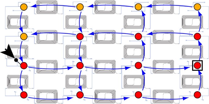
The layout of our chip can be seen in Fig. 1, showing a 16-node square mesh reservoir that contains multiple feedback loops in the network20. Underneath, the actual chip design is visible. The connections consist of 2 cm length low-loss spirals (1.2 dB loss per spiral) corresponding to an interconnection delay of around 280 ps. These delay lines have the sole purpose of bringing the reservoir time scale down to the range that can be addressed by our measurement equipment, that is, sample rates between 125 Mbit s−1 and 12.5 Gbit s−1. A crucial advantage of our design is that by trivially eliminating these delay lines, speeds of up to several hundreds of Gbit s−1 are possible at extremely compact footprints (for example, a 40 times reduction in interconnection lengths down to 500 μm, is trivially possible with the current design. A further reduction to allow for even higher speeds (for example, with interconnections of 200 μm) requires some redesigning of the reservoir.) This is obviously far beyond the bandwidth of for example, the currently available modulators and detectors, but illustrates the way in which this approach is future-proof.
The footprint of the reservoir is 16 mm2, mostly because of the size of the spirals. To ensure low losses, these spirals were shallow-etched waveguides with a bending radius of 40 μm. A chip with shorter interconnections for higher speeds would allow the use of spirals with deep-etched waveguides, which show higher losses (1.36 dB cm−1) but have smaller footprint as the bending radius is around 5 μm21. This could further reduce the size. Coupling and splitting between the nodes is done with a combination of 1 × 2 and 2 × 2 multimode interferometers with very low insertion loss and broadband operation over the wavelength range of the grating couplers used to couple light on and off chip. Note that these MMIs are again purely passive components and only serve to split or combine the light. The loss per grating coupler is 5–6 dB22. The chip is made on a Silicon-on-Insulator (SOI) platform, (through http://www.epixfab.eu), which uses the manufacturing tools from the semiconductor electronics industry. This holds the promise for mass production at low cost. Also, the high index contrast of SOI allows for a much smaller footprint than what is possible in other material platforms21. Making active components in SOI is a topic of ongoing research as silicon has an indirect bandgap23,24, but as our reservoir is passive we can take full advantage of the maturity of silicon processing technology. Also, since the reservoir is passive, the magnitude of the eigenvalues of the weight matrix is smaller than unity.
Boolean operations with memory
In our experiments, we have sent an optical stream of 10,000 bits (modulated on a wavelength of 1,531 nm at the maximum transmission of the grating couplers) into one node of our chip (indicated by the thick black arrow in Fig. 1), and we measure the response at the 11 nodes marked with a red dot. The other five nodes had output powers below the noise floor (around 40 dBm or 100 nW) of our erbium-doped fibre amplifier. More nodes could be measured by amplifying the input signal and by using more efficient couplers to and from the chip. The amplified responses were measured using an optical sampling scope and saved to a computer where they were used for offline training (note that although the training is offline and therefore slow, it only needs to be performed once before the task and not during the task itself). The readout weights were trained such that the output follows a certain desired binary output function, for example, the XOR of the previous bit and the bit before that, x[−1] XOR x[−2]. Note that despite its apparent simplicity, this XOR task with memory is considered to be a hard problem in machine learning, as it cannot be solved by mere linear regression on the inputs, but a result of 25% is, however, possible as a suboptimal solution (in this case one out of four solutions is constantly misclassified).
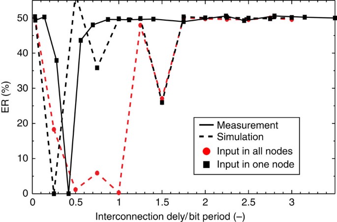
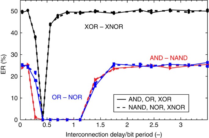
As a performance metric, we use the error rate (ER), that is, the percentage of differences between the trained output and the desired output. Note that the time scale of the reservoir determines how much memory it has of past input signals. Since in our photonic reservoir this time scale is determined by the interconnection delay, we report ER as a function of the (interconnection delay)/(bit period) ratio. In our experiment, the value of the interconnection delay was 280 ps and the bitrate was scanned from 0.125–12.5 Gbit s−1. Figure 2 shows that for a (interconnection delay)/(bit period) ratio of 0.4, we get a good performance for x[−1] XOR x[−2]. We have also simulated our network and find a similar optimal ER, but at a slightly different value of the (interconnection delay)/(bit period) ratio. This can be explained by the fact that the response of the photonic reservoir depends strongly on parameters for which the exact values are unknown, for example, the exact waveguide length and the corresponding phase changes. However, by driving more than a single network input, a wider basin of good performance can be achieved. This is illustrated by simulation results in Fig. 2 for our 16-node network. This basin can be further enlarged by scaling to larger networks and by optimizing the (relative) magnitudes of the input signals in the different nodes. The regime of zero errors in the experiment was obtained for a periodic bit pattern length of 104 bits, which leads to a lower limit of the measurable bit error rate of at least 10−4. Obviously, for practical applications, it will be important in follow-up work to quantitate how much below 10−4 this bit error rate is, to see whether it can compete against alternative approaches. For this, larger reservoirs will need to be studied as well.
Very important to note is that our generic network, which was not at all specifically optimized and designed for a 2-bit XOR with one bit delay, can also solve the XOR of many different bit combinations (Fig. 3), as well as the easier (linearly separable) other Boolean operations on past inputs (Fig. 4). Thanks to the RC principle, this merely requires training a new set of readout weights.
Since no other intrinsic timescales exist in the reservoir, the optimization of interconnection delays only relates to the desired memory, that is, a single optimum exists for all Boolean functions on certain past input bits, demonstrating the general applicability of the RC paradigm. Since the optimum exists for certain (interconnection delay)/(bit period) ratios, chips can easily be designed to handle very high speeds. For example, speeding up the input signal to 100 Gbit s−1 requiring a ratio of 0.5 needs a delay of 50 ps (corresponding to a waveguide length of around 0.5 mm), which is perfectly feasible. Moreover, since that delay line would be much shorter than the 2 cm used here, it will be easier to fabricate and measure larger networks.
Nonlinear readout
For most tasks, including XOR, reservoirs must be able to perform nonlinear transformations of their inputs. However, our reservoir itself is passive and does not contain any nonlinearity. What we exploit here is the intrinsic nonlinearity of the photodetectors, which essentially square the magnitude of the complex representation of the coherent light signal. The actual readout implementation, that is, taking the weighted sum of the states, is currently performed electronically and offline, that is, not in real time. However, it is conceptually easy to also implement this linear combination of states in the optical domain, where a set of variable optical attenuators or modulators implement the weights.
To further prove the point that the nonlinearity in the readout is crucial in a passive reservoir, the simulation results of Fig. 5 show that with a purely linear readout operating on complex values, the performance on the XOR task drops dramatically. It also shows that, for this binary task, taking the norm of the magnitude yields equally good results as when taking the square. Similar results were obtained for other types of nonlinearities at the readout (not shown). This indicates that, for an all-optical readout implementation (that is, in which there would be no photodetectors operating on the states), the states would have to be routed through a nonlinear optical component before linearly combining them, for example, in an optical combiner.
Header recognition
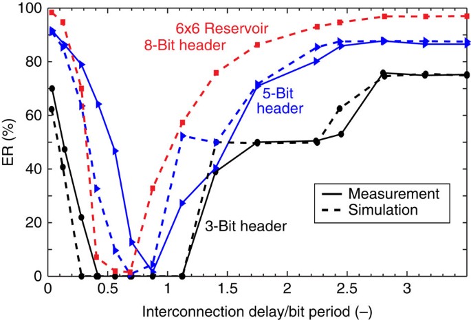
Using the exact same chip and experimental setup as for the Boolean tasks with memory, we also experimentally and theoretically investigated the task of header recognition. Figure 6 shows that with the current chip, we can recognize headers with lengths up to 5 bits. Again, simulation results and experimental results show similar trends, with the differences attributed to phase variations during fabrication. For a larger chip of 6 × 6 nodes, simulations show that it is possible to recognize 8-bit headers. Just as in the previous task, the dominant design parameter is the ratio (interconnection delay)/(bit period), so the system is trivially scalable to speeds >100 Gbit s−1 by shortening the delay lines.
Classification of spoken digits
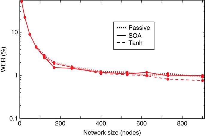
In a previous paper, we investigated the most important properties of photonic reservoirs by means of simulations for an isolated spoken digit recognition task19. The reservoir employed there was a network of coupled semiconductor optical amplifiers. By working at an optimal delay and in the coherent regime, better results than with classical real-valued reservoirs in software were achieved. To compare the passive chip with our previous work, Fig. 7 shows theoretically that we can reach a similar performance to the SOA chip with the exact same passive silicon network we used for the digital tasks above. Due to the unavailability of sufficiently high-speed analogue arbitrary waveform generators, we were unable to test this experimentally, but the good correspondence between theory and experiment for the digital tasks leads us to conclude that the same architecture can also be used to solve analogue signal classification tasks.
Discussion
We have proposed a novel chip-based architecture for photonic RC that uses passive silicon chips and in which the nonlinearity is implemented in the readout layer converting complex amplitudes to intensities. The single generic chip was shown to be capable of solving both digital tasks (like Boolean operations with memory and header recognition) and analogue tasks (isolated digit recognition). The reservoir processing itself does not consume any power, and currently its speed is completely dominated by the input/output speeds, that is, by the modulators and detectors. Internally, the time scale of the network is set by the optical delay, which is easily scalable to perform Boolean operations in the range of several hundreds of Gbit s−1. In addition, given the transparency of the chip over a wide bandwidth, one could, in principle, use dense wavelength division multiplexing methods to have many independent processing channels handled by a single chip. Given the good performance of the same chip on both analogue and digital tasks, this opens the way for a completely novel type of ultrahigh-speed low-power optical information processing, for applications such as optical regeneration/channel equalization1, time series prediction and feature extraction.
Methods
Theoretical model
The model used to describe the optical behaviour of the chip consists of a time-domain approach where a complex-valued envelope E(t) of the signal with carrier frequency  is propagated through a passive network. Taking into account effects like a finite propagation time τ, combined with a waveguide loss α and phase change of ΔΦ, the transmission through the interconnections is modelled by19
  . Splitters and combiners are considered to be lossless and are simply modelled by division of the power by a factor 2 and complex in-phase addition, respectively.
Similar to the experiment, we use the 16-node square mesh reservoir shown in Fig. 1, of which the details are provided in Vandoorne et al.20 The conversion of the aforementioned single component models to a description of the full system for this topology is done using the network simulation software as described in Fiers et al.25 More in particular, as light can be considered to pass instantaneously through the idealized splitters and combiners compared with the latency induced in the delay lines, we concatenate their individual scatter matrices in one big S-matrix. Based on the connection matrix C of the circuit, one can then transfer at each time step the output of the delay lines to the inputs of the subsequent delay lines using an effective connection matrix C’ of the whole circuit, that takes the influence of the splitters and combiners into account. For further details, we refer to Fiers et al.25
Example waveforms collected at the reservoir nodes
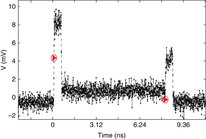
By way of illustration, Fig. 8 shows the output collected at a node (the red node surrounded by a black square in Fig. 1) next to the input node, for an input signal at 2 Gbits s−1 consisting of 16 ‘one’ bits surrounded by ‘zero’ bits. The two red markers indicate the duration (8 ns) of 16 bits. For this particular node, there are two relevant paths from input to output, each with a slightly different delay, and the recorded waveform clearly shows three stages, corresponding to the presence of only the signal from the fast route, the presence of the signal from both paths and the presence of the signal from only the slow route. Destructive interference between both signals is clearly visible in the middle segment, proving that the chip operates in a coherent regime. The delay difference between the two paths is estimated to be 560 ps±7.8 ps (one sample) from the time duration of the ones without interference.
2-bit Boolean task
In measurement and simulation, the 10,000 bits are divided into 10 sets of 1,000 bits used in turn for training and testing through fivefold cross-validation and ridge regression to avoid overfitting. After training the readout weights on the training bit stream, both the tested output (which consists of applying those weights to the states of the reservoir of the test bit stream) and desired output are sampled at the middle of the bit period and a threshold is applied at the middle of the bit amplitude. These two bit streams are then compared to determine the performance of the system, yielding an error rate. The desired bit stream is constructed from the input bit stream depending on the Boolean operation that needs to be solved. The measured 11 reservoir states are padded initially with zeros depending on the signal frequency and the physical interconnection distance from the input node in Fig. 1.
Header recognition task
The setup for this task is similar to the one for the 2-bit Boolean task, but the readout uses a winner-take-all approach. For x-bit header recognition, 2x classifiers have to be trained, one for each possible header. A classifier should give +1 at the last bit of its header, −1 otherwise. After training the readout weights on the training bit stream, both the tested output and desired outputs of all classifiers are sampled at the middle of the bit period and the classifier with the highest response wins. The ER is also here the percentage of differences between the trained output and the desired output.
Isolated digit speech recognition task
Isolated spoken digits, ‘0’ to ‘9’, have to be classified20. In the data set, these words are each spoken 10 times by five female speakers, giving 500 samples, taken from the TI46 speech corpus26. For speech recognition, some pre-processing of the raw speech signal is commonly performed. These methods involve a transformation to the frequency domain and a selective filtering based on known psychoacoustic properties of the human ear and/or spectral properties of speech. For the experiments in this paper, we used the Lyon ear model27. To shorten the simulation time, a decimation of the input signals with a factor of 128 was also applied. We obtain the output by training 10 distinct linear classifiers, one for each digit. Each trained output should return the value +1 whenever the corresponding digit is spoken and −1 otherwise. During testing, a winner-take-all approach is used to determine which word was spoken. The word ER, which is (Nnc/Ntot), with Nnc the number of incorrectly classified samples, and Ntot the total number of samples, determines the performance. Since it is possible to achieve a word ER very close to 0%, babble noise from the NOISEX database was added with a SNR of 3 dB ( http://www.speech.cs.cmu.edu/comp.speech/Section1/Data/noisex.html). The results are always averaged over 10 runs. We used ridge regression to avoid overfitting and fivefold cross-validation to make our results more robust28. This processing was done with a freely available toolbox ( http://www.reslab.elis.ugent.be/rctoolboxv1.0).
SOI
The passive reservoir was fabricated through http://www.epixfab.eu on a SOI wafer with 193 nm deep ultraviolet lithography29. The SOI structure was designed with a top silicon layer of 220 nm and a buried oxide layer of 2 microns. The waveguides are mono mode and only support TE polarization.
Measurement setup
The coupling to and from the chip happens with a vertical fibre setup22. A periodic pattern of 10,000 bits was generated with an Anritsu MP2101A pulse pattern generator. This signal was fed to an amplitude modulator from JDSU onto an optical signal coming from a Finisar (Syntune) S7500 widely tunable laser (line width 5 MHz, active coherence control with wavelength stability significantly below 1 pm h−1).The measured signal was first amplified with a Keopsys erbium-doped fibre amplifier, before being filtered and coupled in the chip. The periodic patterns of the different outputs were detected sequentially with a LeCroy WaveExpert 100H and a 112 Gbit s−1 photodiode from Fraunhofer Gesellschaft. A specific header sequence allowed us to temporally realign the different output channels before processing them in a computer.
Additional information
How to cite this article: Vandoorne, K. et al. Experimental demonstration of reservoir computing on a silicon photonics chip. Nat. Commun. 5:3541 doi: 10.1038/ncomms4541 (2014).
References
Jaeger, H. & Haas, H. Harnessing nonlinearity: predicting chaotic systems and saving energy in wireless communication. Science 304, 78–80 (2004).
Maass, W., Natschlager, T. & Markram, H. Real-time computing without stable states: a new framework for neural computation based on perturbations. Neural. Comput. 14, 2531–2560 (2002).
Hammer, B. & Steil, J. J. inEuropean Symposium Artificial Neural Networks (ESANN) 357–368 (2002).
Pearlmutter, B. Gradient calculations for dynamic recurrent neural networks: a survey. IEEE Trans. Neural Netw. 6, 1212–1228 (1995).
Legenstein, R. & Maass, W. What makes a dynamical system computationally powerful? New Directions in Statistical Signal Processing: From Systems to Brains 127–154MIT Press (2007).
Maass, W., Joshi, P. & Sontag, E. D. Computational aspects of feedback in neural circuits. PLoS Comput. Biol. 3, e165 (2007).
Skowronski, M. D. & Harris, J. G. Automatic speech recognition using a predictive echo state network classifier. Neural Netw. 20, 414–423 (2007).
Antonelo, E. A., Schrauwen, B. & Stroobandt, D. Event detection and localization for small mobile robots using reservoir computing. Neural Netw. 21, 862–871 (2008).
Wyffels, F. & Schrauwen, B. A comparative study of reservoir computing strategies for monthly time series prediction. Neurocomputing 73, 1958–1964 (2010).
Jaeger, H. Short Term Memory in Echo State Networks. Technical Report 152 (GMD, Berlin, 2001).
Verstraeten, D., Schrauwen, B., Suykens, J. A. K., Stroobandt, D. & Vandewalle, J. inInternational Symposium on Nonlinear Theory and its Applications (NOLTA) 101–104 (2008).
Fernando, C. & Sojakka, S. Pattern recognition in a bucket. Adv Artif Life 588–597 (2003).
Jones, B., Stekel, D., Rowe, J. & Fernando, C. inIEEE Symposium on Artificial Life (ALIFE) ’07 187–191 (2007).
Appeltant, L. et al. Information processing using a single dynamical node as complex system. Nat. Commun. 2, 468 (2011).
Brunner, D. et al. Parallel photonic information processing at gigabyte per second data rates using transient states. Nat. Commun. 4, 1364 (2013).
Larger, L. et al. Photonic information processing beyond turing: an optoelectronic implementation of reservoir computing. Opt. Express 20, 3241–3249 (2012).
Duport, F., Schneider, B., Smerieri, A., Haelterman, M. & Massar, S. All-optical reservoir computing. Opt. Express 20, 22783 (2012).
Martinenghi, R., Rybalko, S., Jacquot, M., Chembo, Y. & Larger, L. Photonic nonlinear transient computing with multiple-delay wavelength dynamics. Phys. Rev. Lett. 108, 244101 (2012).
Mesaritakis, C., Papataxiarhis, V. & Syvridis, D. Micro ring resonators as building blocks for an all-optical high-speed reservoir-computing bit-pattern-recognition system. J. Opt. Soc. Am. B 30, 3048–3055 (2013).
Vandoorne, K., Dambre, J., Verstraeten, D., Schrauwen, B. & Bienstman, P. Parallel reservoir computing using optical amplifiers. IEEE Trans. Neural Netw. 22, 1469–1481 (2011).
Bogaerts, W. & Selvaraja, S. K. Compact Single-Mode Silicon Hybrid Rib/Strip Waveguide With Adiabatic Bends. IEEE Photonics J. 3, 422–432 (2011).
Roelkens, G. et al. Grating-based optical fiber interfaces for Silicon-on-Insulator photonic integrated circuits. IEEE J. Sel. Top. Quant. Elect. 17, 571–580 (2011).
Liu, J., Sun, X., Camacho-Aguilera, R., Kimerling, L. C. & Michel, J. Ge-on-Si laser operating at room temperature. Opt. Lett. 35, 679–681 (2010).
Roelkens, G. et al. III-V/silicon photonics for on-chip and intra-chip optical interconnects. Laser Photonics Rev. 4, 751–779 (2010).
Fiers, M. et al. Time-domain and frequency-domain modeling of nonlinear optical components at the circuit-level using a node-based approach. JOSA B 29, 896–900 (2012).
Doddington, G. R. & Schalk, T. B. Computers—Speech Recognition—Turning Theory to Practice. {IEEE} Spectrum 18, 26–32 (1981).
Lyon, R. inIEEE International Conference on Acoustics, Speech, and Signal Processing (ICASSP) 7, 1282–1285 (1982).
Tikhonov, A. N. & Arsenin, V. I. Solutions of ill-posed problems Winston (1977).
Selvaraja, S. K. et al. Fabrication of photonic wire and crystal circuits in Silicon-on-Insulator Using 193 nm optical lithography. J Lightwave Technol 27, 4076–4083 (2009).
Acknowledgements
The work was supported by the ERC StG project ‘NaResCo’, the IAP project ‘Photonics@be’, a UGent Methusalem Grant and the European Human Brain Project. We thank Jan Vancampenhout and Roel Baets for fruitful discussions and Michael Vanslembrouck for valuable automatization contributions to the measurements.
Author information
Authors and Affiliations
Contributions
K.V. designed the chip and the experiment, performed the experiment and analysed the data. P.M. and G.M. contributed to the measurements; T.V.V. and M.F. contributed to the simulations; D.V. and B.S. contributed to the data analysis; and J.D. and P.B. supervised the work. All authors discussed the results and commented on the manuscript at all stages.
Corresponding author
Ethics declarations
Competing interests
The authors declare no competing financial interests.
Rights and permissions
This work is licensed under a Creative Commons Attribution-NonCommercial-NoDerivs 3.0 Unported License. The images or other third party material in this article are included in the article’s Creative Commons license, unless indicated otherwise in the credit line; if the material is not included under the Creative Commons license, users will need to obtain permission from the license holder to reproduce the material. To view a copy of this license, visit http://creativecommons.org/licenses/by-nc-nd/3.0/
About this article
Cite this article
Vandoorne, K., Mechet, P., Van Vaerenbergh, T. et al. Experimental demonstration of reservoir computing on a silicon photonics chip. Nat Commun 5, 3541 (2014). https://doi.org/10.1038/ncomms4541
Received:
Accepted:
Published:
DOI: https://doi.org/10.1038/ncomms4541
This article is cited by
-
Connectome-based reservoir computing with the conn2res toolbox
Nature Communications (2024)
-
Nonmasking-based reservoir computing with a single dynamic memristor for image recognition
Nonlinear Dynamics (2024)
-
Experimental results on nonlinear distortion compensation using photonic reservoir computing with a single set of weights for different wavelengths
Scientific Reports (2023)
-
Interface-type tunable oxygen ion dynamics for physical reservoir computing
Nature Communications (2023)
-
Thermally-robust spatiotemporal parallel reservoir computing by frequency filtering in frustrated magnets
Scientific Reports (2023)
Comments
By submitting a comment you agree to abide by our Terms and Community Guidelines. If you find something abusive or that does not comply with our terms or guidelines please flag it as inappropriate.

