Mapping a Guided Image Filter on the HARP Reconfigurable Architecture Using OpenCL


1
Department of Electronics and Information Systems, Ghent University, 9052 Ghent, Belgium
2
Department of Telecommunications and Information Processing, imec-IPI-Ghent University, 9000 Ghent, Belgium
*
Author to whom correspondence should be addressed.
Algorithms 2019, 12(8), 149; https://doi.org/10.3390/a12080149
Submission received: 27 June 2019
/
Revised: 23 July 2019
/
Accepted: 25 July 2019
/
Published: 27 July 2019
(This article belongs to the Special Issue High Performance Reconfigurable Computing)
Abstract
:Intel recently introduced the Heterogeneous Architecture Research Platform, HARP. In this platform, the Central Processing Unit and a Field-Programmable Gate Array are connected through a high-bandwidth, low-latency interconnect and both share DRAM memory. For this platform, Open Computing Language (OpenCL), a High-Level Synthesis (HLS) language, is made available. By making use of HLS, a faster design cycle can be achieved compared to programming in a traditional hardware description language. This, however, comes at the cost of having less control over the hardware implementation. We will investigate how OpenCL can be applied to implement a real-time guided image filter on the HARP platform. In the first phase, the performance-critical parameters of the OpenCL programming model are defined using several specialized benchmarks. In a second phase, the guided image filter algorithm is implemented using the insights gained in the first phase. Both a floating-point and a fixed-point implementation were developed for this algorithm, based on a sliding window implementation. This resulted in a maximum floating-point performance of 135 GFLOPS, a maximum fixed-point performance of 430 GOPS and a throughput of HD color images at 74 frames per second.
1. Introduction
Ever since the introduction of the von Neumann architecture there has been a need for growing computing speed. Until around 2015, improved architectural design, faster memories, domain specific accelerators, and high-performance oriented languages enabled computing power to keep up with the most demanding applications. However, the growth is slowing down by the limits of Dennard scaling and Moore’s law. Dennard scaling [1] started to fall off for designs at less than 65 nm due to increasing leakage power and the limit of Moore’s law slows the performance progress to 3% per year [2]. Further significant processing rise should come from designs and innovations which stay abreast of the limits imposed by the physics of today’s electrical circuits and systems.
In this paper, we use a high-performance field-programmable gate array (FPGA), tightly coupled to a fast multicore processor. Architectural innovations include a cache-coherent interface with transparent address translation, high-speed wide communication path and the support of a high-level synthesis language Open Computing Language (OpenCL). In particular, the Heterogeneous Architecture Research Platform (HARP) developed by Intel, is aimed at developing applications on CPU and FPGA, using OpenCL [3,4].
HARPv2, the second generation of the HARP platform, was announced in 2016 and has several architectural enhancements compared to its predecessor, HARPv1 [5]. In this paper, we implement and optimize the guided image filter on FPGA using the HARPv2 platform, taking advantage of Shared Virtual Memory (SVM). The guided image filter was chosen because (1) it is an important filter used in various sensor fusion (e.g., time-of-flight and RGB) methods in image processing and (2) because the algorithm is suited to run on FPGA hardware, but still not too trivial, allowing several performance characteristics to be investigated (e.g., I/O, cache…) [6] and (3) in industry applications, there is a need for guided image filter-based methods running on edge devices (e.g., containing an FPGA) and in the cloud.
The goal of this paper is (1) to benchmark OpenCL on HARP and determine the read bandwidth and cache performance, in particular, performance of the OpenCL cache and FPGA interface unit cache, (2) to implement and tune the guided filter algorithm on HARP based on the obtained benchmarks, (3) to evaluate the performance of the algorithm for real-time processing full-HD video on a high-performance FPGA, for fixed- versus floating-point calculations.
The major contributions of this paper are therefore: the benchmarking tests of OpenCL on HARP; the implementation of the guided image filter on HARP with several performance optimizations (such as channel vectorization, sliding window via shift registers, fixed-point calculations, use of shared virtual memory) and the roofline performance model analysis of the optimized algorithm in floating point versus fixed point.
The remainder of this paper is structured as follows: in Section 2, we give background information on the FPGA and in particular, the HARP platform. A general overview of OpenCL on the HARP platform is given in Section 3. To investigate whether OpenCL can exploit the performance enhancing features of the HARP platform, we perform several benchmarking tests in Section 4. Next, using the performance guidelines for implementing algorithms on an FPGA, we discuss the Guided Filter in Section 5 and we explain the FPGA-specific optimizations that were performed. The experimental results of the Guided Filter on HARPv2 are presented in Section 6 and the related work is discussed in Section 7. Finally, Section 8 concludes this paper.
2. FPGAs and the HARP Platform
FPGAs are an interesting approach to alleviate the limits of technology scaling and application parallelism for several reasons. First, FPGAs operate at a low clock speed (100 ) which is much lower than typical GPU frequencies. Second, FPGAs operate as a hardware-implemented algorithm. In contrast with von Neumann architectures, FPGAs have no fetch and decode stage when executing instructions, thereby bypassing an important instruction overhead. Operations are organized according to the data dependencies in the algorithm, creating a dataflow architecture. Typically, loops are partially or completely unrolled, and the iterations are converted into long pipelines fed by streams of data. In contrast with parallel single instruction multiple data (SIMD) architectures where a single instruction operates on multiple data elements, a pipelined loop is a multiple instruction single data (MISD) architecture where multiple instructions are executed on a single stream of data elements [7]. The difference is that in a MISD design data dependencies may occur between adjacent loop iterations, which otherwise preclude effective parallelization. Pipelines of unrolled loops may become very long, delivering one new result per cycle at the end of the pipeline. A continuous stream of data therefore will realize a speedup proportional to the number of stages in the pipeline. Furthermore, a pipelined design may be parallelized to operate on multiple independent data streams, leading to an organization with horizontal and vertical threads. Consequently, the speedup is multiplied by the number of parallel operating components and this may compensate several times the loss in clock speed. Finally, the FPGA model of computation does not rely exclusively on parallel SIMD operations. The best performance is obtained from pipelined computations on a long stream of data. Using Flynn’s topology [7], this model can be represented by a MIMD/SIMD architecture, in the sense that multiple instructions streams operate simultaneously on multiple pipelined data streams.
2.1. The HARP Platform
The HARP is a CPU-FPGA platform that is developed by Intel to spur research in CPU-FPGA heterogeneous computing platforms. In a first stage, in 2015, an Intel Xeon CPU was combined with an Altera Stratix V FPGA in a discrete configurable platform (DCP). These two chips were connected using a single Intel QuickPath Interconnect (QPI) channel, and shared DRAM memory. For clarity, this first-generation HARP platform will be referred to as HARPv1. In a later stage, in 2017, the second generation of HARP was introduced, here mentioned as HARPv2. HARPv2 consists of a 14 core Intel Broadwell Xeon CPU combined with an Intel Arria 10 GX1150 FPGA [8]. In HARPv2, the CPU and FPGA also share DRAM memory, but they are connected through one QPI channel and two Peripheral Component Interconnect Express (PCIe) channels. Instead of a discrete configuration of 2 separate chips, as in HARPv1, HARPv2 combines both chips in a Multi-Chip Package (MCP) [5]. Besides the single DDR memory, the FPGA has a coherent cache and physical to virtual memory address translation Intellectual Property (IP) core.
The CPU and the FPGA in the HARPv2 platform are connected through three physical channels: one QuickPath Interconnect (QPI) channel and two Peripheral Component Interconnect Express (PCIe) channels. QPI is an interconnect technology, developed by Intel, that connects processors in a distributed shared memory style [9]. PCIe, on the other hand, is a general purpose I/O interconnect defined for a wide variety of computer and communication platforms. The HARPv2 uses a PCIe Gen3x8 interconnect. This indicates that the PCIe connection uses the third generation PCIe technology, and has a bit width of 8 bits.
The QPI channel has 16 data connections, and therefore a bit width of 2 B. Its maximum transfer rate is 6.4 GT/s. This results in a maximum, one-way bandwidth of 12.8 GB/s [9]. Similar calculations can be done for the PCIe channels. The used PCIe connection is of third generation, and has a bit width of 8 bits. However, compared to the QPI channel, the PCIe uses a less efficient data encoding scheme, which results in a physical channel with an efficiency of 98.5%. Therefore, for every 130 bits sent, only 128 bits are useful. The maximum amount of transfers per second equals 8 GT/s. This results in a maximum raw bandwidth of 98.5% × 1 byte × 8 GT/s = 7.88 GB/s.These characteristics are shown in Table 1. The theoretical maximum unidirectional bandwidth of both QPI and 2 PCIe connections combined is 28.56 GB/s. The effective measured bandwidths are 17.02 GB/s for separate reads or writes of 64 byte lines. A combined read/write benchmark such as memcopy yields 26.7 GB/s, i.e., 13.35 GB/s for reads and writes, respectively.
Based on previous calculations, one could conclude that the HARP platform can obtain read- and write-bandwidths up to 28.56 GB/s. Above results are, however, theoretical bandwidths and they do not account for packet overhead and other effects. Therefore, the maximum bandwidth that can be achieved will be lower, and can also vary for different types of data transfers.
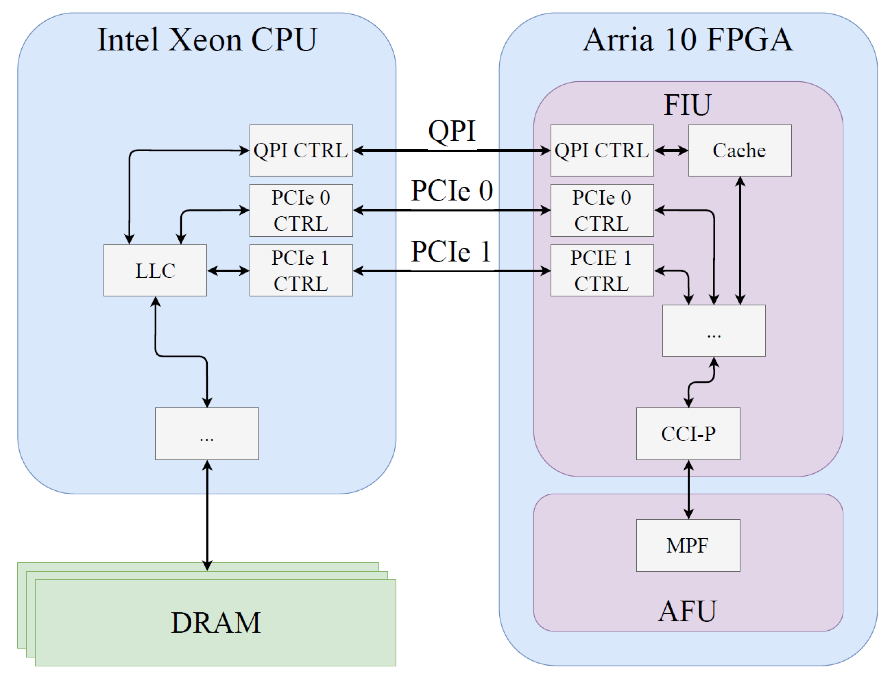
An FPGA is configured by an FPGA bitstream. In the HARPv2 platform, the FPGA bitstream consists of two parts: the FPGA Interface Unit (FIU) and the Accelerator Functional Unit (AFU). The FIU contains Intel-provided IP. It implements I/O control, power and temperature monitoring and partial reconfiguration, and it provides one or more interfaces to the AFU. The AFU, on the other hand, consists of programmer-defined FPGA code and determines the functionality of the FPGA. The architecture of the FIU and the AFU, and their internal structure is shown in Figure 1.
2.2. Core-Cache Interface
An important function of the FIU is to abstract the QPI and PCIe channels by providing a transparent interface to the AFU. Therefore, a developer does not need to program low-level details of the physical communication channels. This interface is the Core-Cache Interface (CCI-P). The CCI-P abstracts the three physical channels in the HARP platform by mapping them onto so-called virtual channels. PCIe 0 and 1 are mapped onto virtual channels VH0 and VH1 (virtual channels with high latency), and QPI to VL0 (virtual channel with low latency). A fourth virtual channel, VA (virtual auto), combines the three physical channels into one virtual channel and automatically selects the appropriate physical link during execution by making use of virtual channel (VC) steering logic [10]. The cache-coherent fabric also supports shared virtual memory, which greatly reduces the data transfer overhead. A detailed description of the QPI-based cache-coherent fabric is presented in [3].
2.3. FPGA Cache
The FIU core not only contains the CCI-P, it also provides an IP cache in the FPGA, for the QPI channel, see Figure 1. This cache has a total capacity of 64 KiB, and is direct-mapped with 64 B cache lines. As the FPGA cache is included in the cache coherence domain of the CPU, the data in the FPGA cache is coherent with the CPU cache and the DDR memory.
Because of the expanded cache coherence domain, AFU memory requests can be serviced at three different memory levels. The lowest latency and highest bandwidth is obtained when reading from the FPGA cache itself. In this case, no read request to the CPU is required. If the FPGA cache does not contain the requested cache line, the next memory level to be addressed is the CPU Last Level Cache (LLC). This results in a higher latency and lower bandwidth than when reading from the FPGA cache. The highest latency and lowest bandwidth is obtained when both the FPGA cache and the CPU LLC read requests result in a miss. In this case, the read request is serviced by the DRAM. The FIU supports two programming languages: Hardware Description Language (HDL) and OpenCL. The OpenCL code is compiled into HDL by the Intel OpenCL compiler and the resulting HDL code is synthesized into a bitstream using Intel Quartus.
3. OpenCL on HARPv2
OpenCL [11] is a framework, developed by Khronos Group, for programming heterogeneous computing architectures. Moreover, it provides an API through which either task-based or data-based parallelism can be defined. Even though OpenCL was originally designed for GPU-programming, it is available for all types of accelerators. OpenCL facilitates the development of software for heterogeneous computing architectures on two different levels. On the one hand, it provides an API through which the accelerator device can be controlled. On the other hand, a C-based programming language is defined that is used to program the accelerator itself [12].
An OpenCL application consists of two parts: the host and the kernel. Host code is executed on the CPU, while kernel code is executed on a selected accelerator. Both components have a different function in the OpenCL framework. The host can be considered to be the executive part of an OpenCL application as it manages the kernel. It is responsible for providing data to the kernel, invoking the kernel etc. The kernel, on the other hand, is a function executed on the accelerator. Therefore, it typically consists of critical code that is executed more efficiently on the accelerator architecture. A host can call multiple kernels on different accelerator devices.
An OpenCL kernel is defined as a function that is executed on the accelerator. An OpenCL kernel definition has the following structure: __kernel void <kernel name>(<input parameters>). A kernel function is indicated by the __kernel keyword. Because an OpenCL kernel cannot directly return a value, it is always accompanied by the void keyword. The <kernel name> keyword indicates the name of the kernel, and the <input parameters> indicates that a kernel function can be passed a variable number of parameters. Kernel parameters can be passed either by value or by reference.
3.1. OpenCL Kernel Types
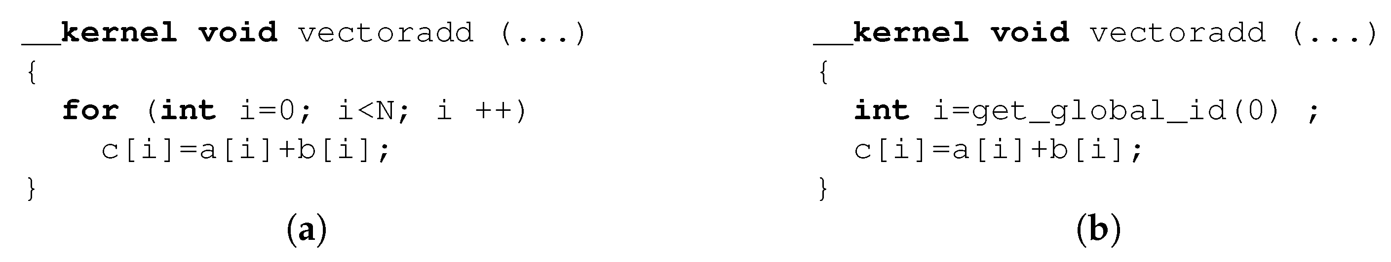
OpenCL kernels can be subdivided into 2 different types: single work-item kernels and NDRange kernels. In a single work-item kernel, only one instance of the kernel is executed, while in an NDRange kernel, multiple instances of the kernel are executed in parallel corresponding to the iteration space of a n-dimensional loop, i.e., the N-Dimensional Range. The difference between these two types of kernels is illustrated by the examples of Figure 2. In both code fragments, the sum of vectors a and b is calculated and written to vector c. Even though both kernels calculate the same vector-summation, they execute in an entirely different way. The code in the single work-item kernel is implemented as a single compute unit (the functionality of the kernel is implemented only once, and this single implementation processes all data). Because the implemented for-loop iterates serially over the indices i, only a single element of vector i will be calculated at each time step. An NDRange kernel, on the other hand, consists of multiple compute units, allowing execution in a SIMD way. As can be seen in Figure 2b, no for-loop is present. Instead of sequentially calculating the sum of vectors a and b, the OpenCL framework assigns a specific index to each compute unit by using the function get_global_id(0).
Both kernel types have different characteristics and the decision to choose one of both heavily depends on the hardware: a single work-item kernel is not suited for a GPU because only one GPU-core is used while all others are idle. An NDRange kernel allows simultaneous execution of different compute units on different cores. The FPGA can implement data-level parallelism; however, single work-item kernels are preferred because it enables pipeline parallelism. In pipeline parallelism, a computation is split into different pipeline stages. Intermediate results are stored in registers, thereby splitting lengthy calculations in several smaller computation steps. Several iterations are then executed simultaneously in different pipeline stages. Such pipelined implementation often leads to a high performance on FPGA.
3.2. OpenCL Kernel Programming
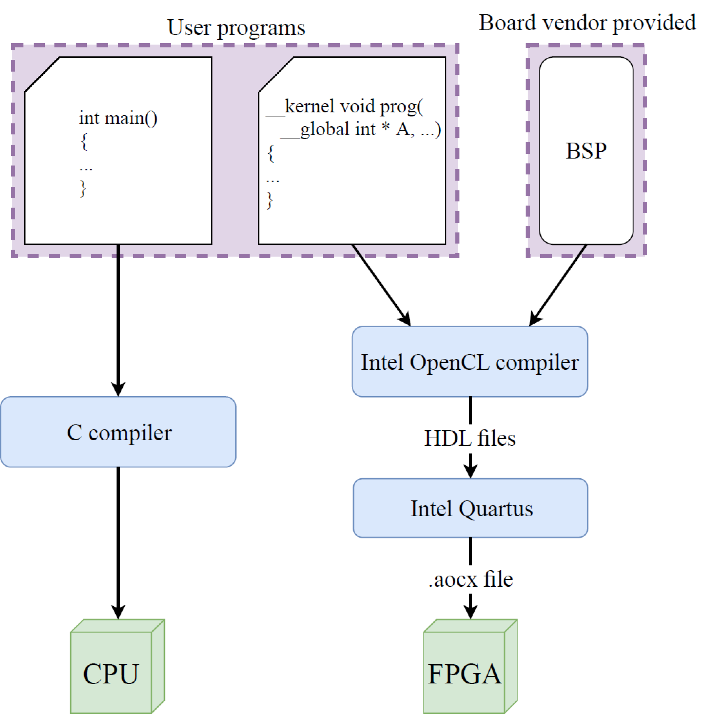
The main tasks of an OpenCL host are providing data and invoking the OpenCL kernel. This, however, requires certain API-calls to be made. Some examples are requesting access to the accelerator platform, creating the OpenCL kernel or creating a command queue through which kernel commands can be sent. Therefore, calling a kernel is not as straightforward as just calling a function in C. Altera, now Intel FPGA, adopted the framework by developing a Software Development Kit (SDK) for its FPGA platforms. This SDK is called Intel FPGA SDK for OpenCL, and is built on top of the Intel Quartus software. Intel Quartus is the software package that enables FPGA development for Intel FPGAs in an HDL [13]. Developing OpenCL applications for a CPU-FPGA heterogeneous computing platform is done by programming the CPU in C/C++ and the FPGA in OpenCL. Both languages are higher level languages, in which the specifics of the underlying hardware are concealed. In order to incorporate the hardware information, a Board Support Package (BSP) is defined. The BSP contains logic information, memory information and I/O controllers to communicate with the CPU.
An FPGA bitstream is generated in 2 major steps, as depicted in Figure 3. In a first step, the OpenCL kernel is compiled to HDL code by making use of the Altera OpenCL (AOCL) compiler. The hardware information of the FPGA is incorporated in the generated HDL code by making use of the BSP. In the second step, an FPGA bitstream is generated based on the compiled HDL code. In this step, all necessary implementation details, such as selecting the appropriate FPGA frequency, are determined by the Quartus toolchain. This results in an Altera OpenCL executable (.aocx) file that contains the FPGA bitstream. The host code, on the other hand, is compiled using an appropriate C compiler.
As indicated in the previous sections, there are two types of OpenCL kernels: single work-item kernels and NDRange kernels. In the Intel FPGA SDK for OpenCL, both types of kernels are implemented completely different. When compiling an NDRange kernel, the FPGA implements a GPU-like architecture in which several threads execute simultaneously. This implementation, however, does not make use of pipeline parallelism. Single work-item kernels, on the other hand, are implemented in a pipelined fashion.
The iterations in a pipelined loop execute in lockstep using several s consecutive stages. Multiple consecutive iterations can be executed each in separate stages. The Initiation Interval (II) is the minimal number of cycles to start successive iterations. This interval is subject to data or control dependencies or lack of resources, e.g., memory ports. The II of a pipelined loop largely determines the performance. The desired value for the II is one. In this case, a new loop iteration can be issued every clock cycle, and the implemented hardware will be used 100% of the time. This leads to the optimal performance. If the II, however, is higher, a lower performance will be obtained. For an II of two, only one loop iteration will be started every two clock cycles. Therefore, each pipeline stage will only be used 50% of the time, and the loop will take two times as much time to finish. An II of three leads to a usage of 33.33% and an execution time that is three times higher, and so forth. A large value of II can have several possible causes. Some examples are I/O delay, a limited number of resources or dependencies in the algorithm. When developing a single work-item OpenCL kernel for FPGA, the purpose should always be to obtain an II of one for implemented loops. Higher values lead to a lower use rate and therefore a lower performance.
Three main development phases are distinguished when developing an OpenCL project with the Intel FPGA SDK: the emulation phase, the performance tuning phase and the execution phase. In the emulation phase, the behavior of the kernel is verified by emulating the code on a CPU. In the performance tuning phase, performance bottlenecks are identified by inspecting compilation and profiling reports. In the execution phase, the performance of the OpenCL kernel is analyzed by executing the kernel on the FPGA platform. Since the performance tuning phase is the most critical stage for improving the performance, this will be discussed more in detail in following sections.
3.3. Performance Tuning Phase
After the initial implementation of an OpenCL kernel, the performance of the kernel needs to be improved to run efficiently on the FPGA. Therefore, a performance tuning phase is required in which the performance of the OpenCL kernel is analyzed and improved. The Intel FPGA SDK for OpenCL provides two types of reports that can be used in this phase: compilation reports and profiling reports. During the compilation process, reports of the produced HDL code are generated. These reports contain information on the resource usage of the kernel, the compilation transformations, the initiation interval of loops and so forth. By investigating these reports, more insight in the implemented hardware can be gained. Because of the compilation reports, an early performance analysis can be made, which prevents going through the full, lengthy FPGA development cycle to assess the OpenCL kernel performance.
Six different types of reports can be selected: loop analysis, area analysis of system, area analysis of source, system viewer, kernel memory viewer and summary report. Since this paper focuses on performance programming, only the loops analysis and the system viewer reports will be discussed.
In the loop analysis report all loops in a kernel are listed. For each of the loops, there are four performance indicators: pipelined: indicates whether a loop is pipelined, II: displays the initiation interval in case the loop is pipelined, bottleneck: displays whether or not there is a performance bottleneck and details: explains the cause of the performance bottleneck, if there is one.
A visual representation of the kernel can be found in the system viewer. In this view, the OpenCL kernel is displayed as a control flow graph of basic blocks. A basic block is a is a sequence of statements that is always entered at the beginning and exited at the end. Besides the operation flow, all memory operations to the global DRAM memory are displayed in this report.
3.4. Profiling Reports
The Intel FPGA SDK for OpenCL enables reviewing the kernel’s performance by incorporating the OpenCL Profiler. When generating an FPGA bitstream using the profile-option, the FPGA program will measure and save performance metrics during execution. This enables reviewing the kernel’s behavior, and in this way detecting e.g., causes of a kernel’s poor performance. The profiling information is saved in a .mon-file, and can be viewed through a graphical user interface. For each I/O statement, following performance metrics are shown.
- Stall (%): indicates the percentage of the overall profiled time frame that the memory access causes a pipeline stall. Since a pipeline stall is not desired, the preferable stall-value is 0%.
- Occupancy (%): the percentage of the overall profiled time frame that a memory instruction is issued. In a pipelined implementation, the best performance is achieved when every clock cycle a loop iteration stage can be issued. Therefore, the most desired value for the occupancy is 100%.
- Bandwidth (MB/s): the average memory bandwidth of a memory access.
- Bandwidth efficiency (%): the percentage of loaded memory that is actually used by the kernel. Since data is loaded by reading memory words, it is possible that parts of the loaded word are not used by the kernel. In the optimal case, all loaded data is used. Therefore, an efficiency of 100% is desired.
3.5. Design Exploration Time
OpenCL offers the software engineer an abstraction level well above the bare metal hardware description languages. The synthesis of the hardware is controlled by specific pragmas and the standard programming style of this language. The compiler generates the hardware description and together with it several reports on resources usage, performance and I/O behavior. A design compilation typically runs in the order of minutes. This allows a rapid design exploration based on the performance reports. When the developer is satisfied with the expected performance, the hardware description is mapped onto the FPGA and a bitstream is generated. Hardware generation is a long process, which can take many hours to complete. In the end, the performance of the real design can be profiled and compared with the expected performance reports. The profiling monitors the FPGA in its environment, such as communication with the CPU and off-chip memory. Generally, there is a good correspondence between the measures and expected performers. Therefore, most of the design exploration time goes into the fast prototyping phase with the high-level synthesis language OpenCL.
4. Benchmarking OpenCL Performance on HARP
In this section, we investigate whether OpenCL can exploit the performance enhancing features of the HARP platform. This will be done by several tests that focus on a specific hardware characteristic. In a first test, the HARP read bandwidth will be examined by making use of several OpenCL kernels. Thereafter, the cache performance of the FPGA cache is investigated. Finally, the effect of SVM will be analyzed.
4.1. Bandwidth
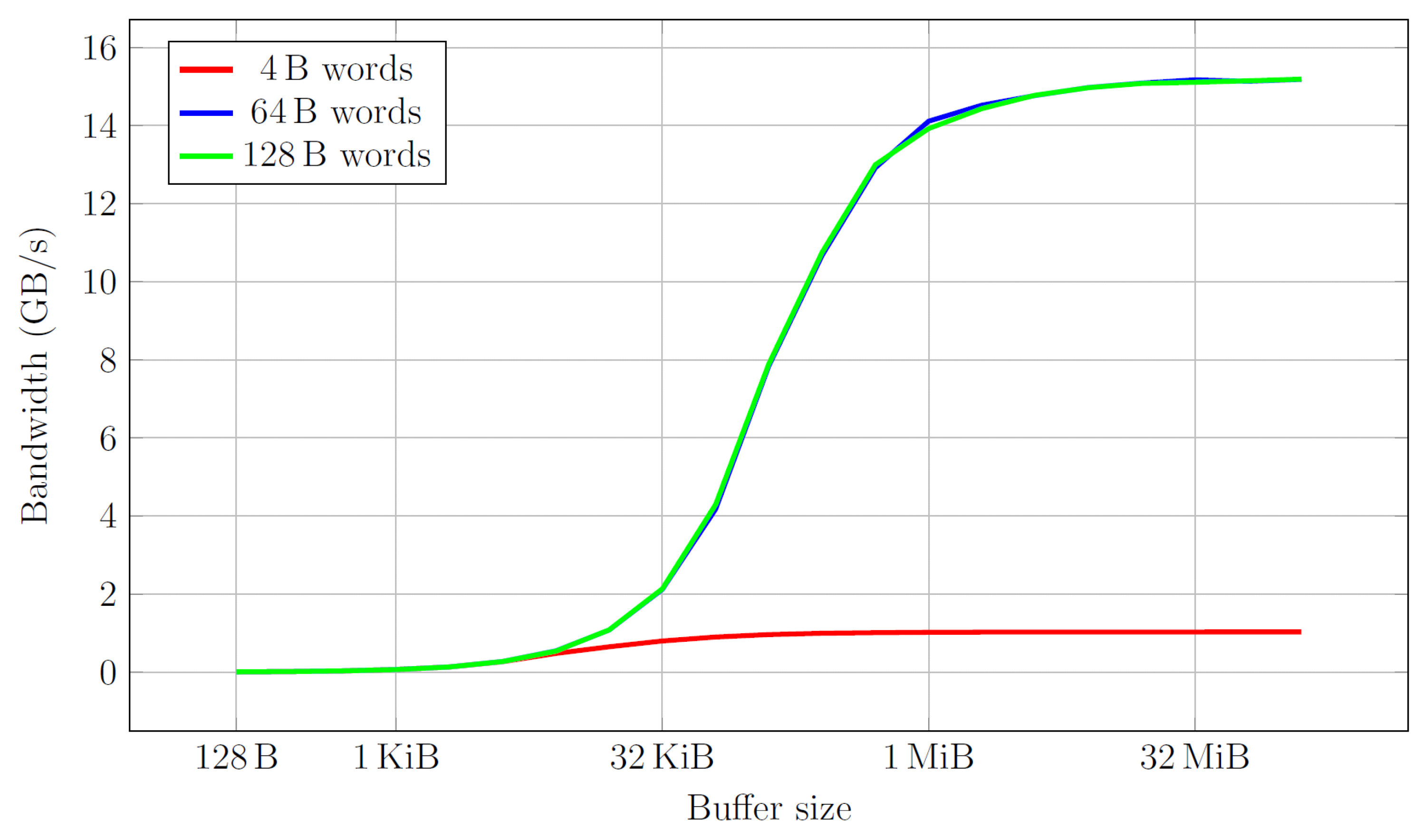
In a first test, the read bandwidth of the HARP platform is investigated by reading a buffer with data widths 4, 64 and 128 bytes and sizes from 128 B to 23 MB. Figure 4 shows the maximum bandwidth for wide buffers is 15 GB/s, whereas small data width buffers (e.g., an array of 4 byte integers) end at 1 GB/s. Furthermore, there is no difference between 64 and 128 data widths, since the cache lines are 64 bytes wide.
Interestingly, the poor bandwidth for small data widths may be alleviated by unrolling the loop 16 times such that each iteration fetches 64 bytes. In that case the measured bandwidth is 14 GB/s.
4.2. FPGA Cache
As explained earlier, the FIU implements a soft IP cache. The responsibility of the FIU cache is preventing memory requests to be passed to DRAM memory. If the requested data is already available on the FPGA itself, a higher bandwidth and lower latency can be achieved. The FPGA cache has a capacity of 64 KiB with 64 B direct-mapped cache lines. In the HARP platform, the Intel Arria 10 FPGA is connected to the processor through one QPI and two PCIe channels. The FIU cache, however, is only implemented for the QPI channel. Therefore, if a memory request is passed to a PCIe-channel, there is no cache look-up and the memory request will be sent to DRAM memory. Since the OpenCL board support package for the HARP platform uses the virtual auto (VA)-channel, a memory request can be assigned to each of the three physical channels. As a result, an FPGA memory request in the HARP platform will not necessarily pass the FIU cache, and cache performance is unpredictable.
4.3. OpenCL Cache
Cache behavior is typically subdivided into two different types: spatial locality and temporal locality. When using spatial locality, data elements are loaded that are located close together in memory. In temporal locality, on the other hand, data is loaded several times within a small time duration. The OpenCL kernel used to test the FIU cache is displayed in Listing 1.
 1  __kernel void
 2  __attribute__ (( task ))
 3  cache_read (
 4    __global volatile ulong8 ∗ restrict src, dst,
 5    unsigned int lines )
 6  {
 7    ulong8 output = ( ulong8 ) (0) ;
 8    for ( unsigned int i = 0; i<ITERATIONS; i ++) {
 9      unsigned int index = i%lines ;
10      output += src[index];
11    }
12    ∗dst = output;
13  }
             Listing 1: Kernel code used to test the cache effectiveness of OpenCL.
The for-loop iterates for a fixed number of iterations, indicated by the constant ITERATIONS. The number of iterations is determined at compile time, and is chosen sufficiently high such that overhead effects become insignificant. The array src is indexed by the variable index = i%lines, running over lines cache lines in a round robin fashion. If lines is, for instance, equal to 4, the first four variables will be repeatedly accessed. This leads to following access pattern: 0, 1, 2, 3, 0, 1, 2, 3, … By using this modulo-operation, temporal locality is enforced, and cache performance can be evaluated. The input parameter lines determines the degree of temporal locality. The pointers src and dst are marked volatile. This keyword indicates that the data to which a pointer points may change over time. Therefore, every time the variable is read, a memory request should be sent. If the volatile keyword is not used, on the other hand, the loaded data is buffered in the OpenCL kernel. In this case, the OpenCL compiler adds a software implemented cache to the FPGA bitstream through which all memory requests pass [14]. When using a hardware-implemented QPI cache, it is, therefore, important to mark src and dst as volatile, such that no software cache prevents the FIU cache to be read. The software cache, however, can be used as a comparison to the FIU cache. Therefore, the kernel cache read was also implemented without using the volatile keyword.
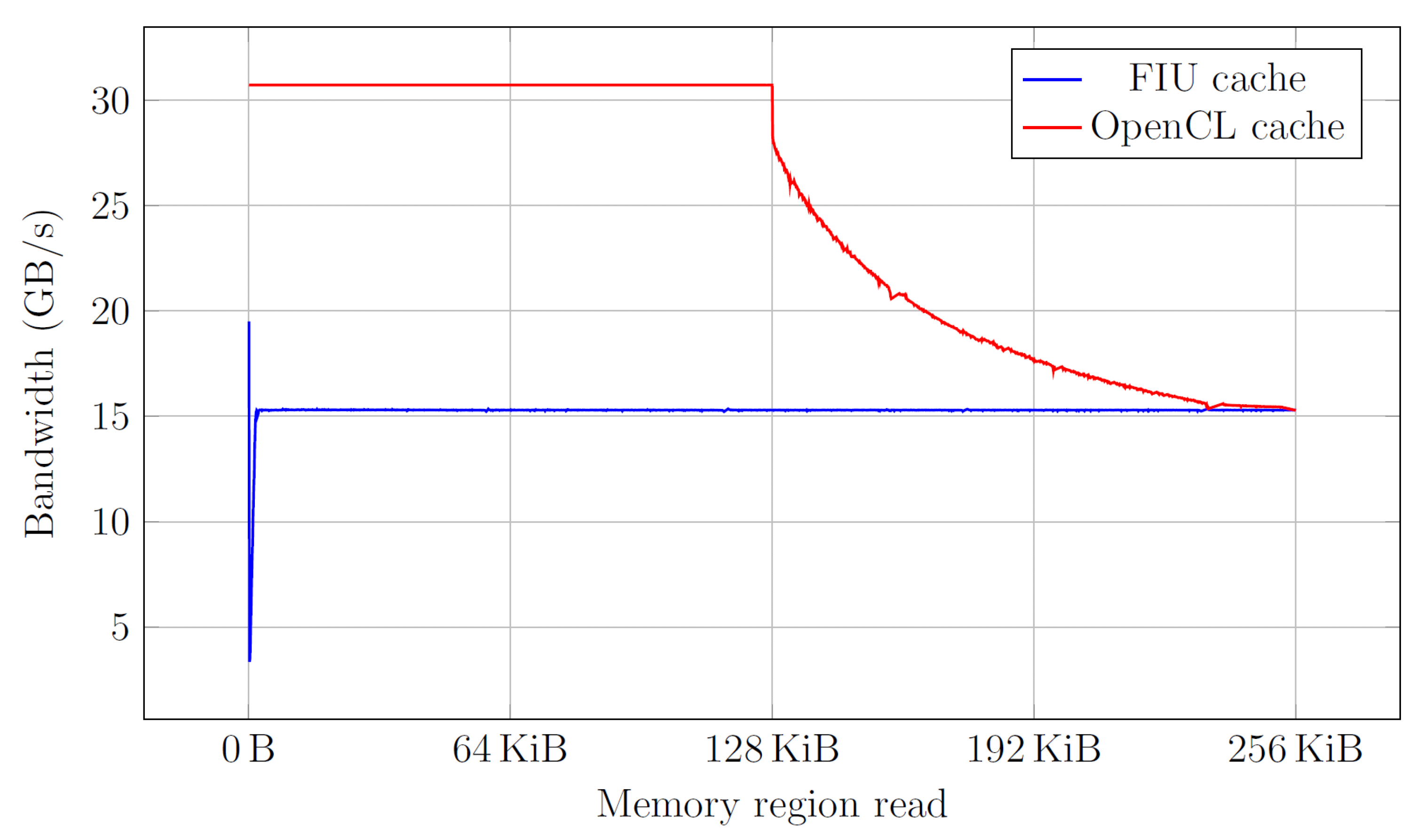
The kernel was developed for both the ulong8 and ulong16 data type. It was synthesized to an .aocx file, which resulted in a clock frequency of 240.6 MHz. The variable lines was varied from 1 to 2048. This resulted in repeated reads of a memory region with size 64 B to 128 KiB for the ulong8 variable, and 128 B to 256 KiB for the ulong16 variable. As the kernels are fully pipelined, every clock cycle a variable is read. Because of the frequency of 240.6 MHz, clock cycle time of 4.16 ns, the requested bandwidth is 15.4 GB/s for the ulong8 vector data type and 30.8 GB/s for the ulong16 vector data type. In Figure 5, the obtained average bandwidths for both kernels are displayed with and without using the volatile keyword.
As can be seen in Figure 5, the OpenCL-implemented cache is able to fulfill the requested bandwidths of 30.8 GB/s. From the graph the size of the OpenCL generated cache core can be derived from the point where the bandwidth drops. When reading ulong8-variables, the OpenCL cache has a size of 64 KiB; when reading ulong16- variables, the cache is 128 KiB large. When the memory region is larger than the cache size, the bandwidth decreases and converges to an asymptotic bandwidth of 9.3 GB/s.
4.4. Shared Virtual Memory
A third aspect that is considered, is the use of SVM. In the OpenCL framework, data is communicated between the host and the kernel by reading from and writing to allocated memory areas. There are two different types of memory areas: memory buffers and SVM.
When using memory buffers, the data is copied to a specially allocated part of the RAM memory that is called a memory buffer. The host can only access memory buffers through the OpenCL API. Moreover, the memory location of the memory buffers depends on the accelerator architecture. In a PCIe-based CPU-FPGA architecture, both the processor and the FPGA have their own DRAM memory. In this type of architecture, the memory buffer is in the FPGA DRAM memory. The data that is in the CPU DRAM is therefore copied from CPU DRAM to FPGA DRAM, after which the FPGA reads from the FPGA DRAM. This is the conventional operation in a traditional PCIe-based CPU-FPGA platform.
In a shared memory architecture such as the HARPv2 platform, on the other hand, both the original data and the OpenCL buffer are stored in the shared DRAM. SVM is a paradigm in which the original data can be accessed by both the OpenCL kernel and by the host. The host and the FPGA can access the SVM-allocated memory area by using conventional memory operations. Therefore, data is not duplicated, as illustrated in Figure 1.
4.5. Benchmark Results
The following results were obtained for the executed benchmarks.
The maximum bandwidth that was achieved in the different tests is 15.73 GB/s. The maximum raw one-way bandwidth of the interconnect is 28.56 GB/s. Due to communication overhead, this raw bandwidth will never be achieved. However, a more detailed analysis on what communication overhead aspects affect the bandwidth would be useful. It was noticed that boosting the bandwidth by making use of the pragma unroll did not achieve good results. When using a custom struct, on the other hand, a high bandwidth was obtained. Therefore, using a struct is recommended when data must be read for which no native data type is available.
In the executed tests, traces of the FIU cache were found. When loading 128 B values, for instance, bandwidths of over 30 GB/s were obtained. Because this bandwidth exceeds the physical limits of the interconnect, the FIU cache was presumably used. However, it is only in certain cases, and only for a couple of measurements, that the FIU cache was effective. In all other cases, the achieved bandwidths do not satisfy the requested bandwidths. A possible cause for this problem is the virtual auto channel, which selects the physical channel without taking cache locality into account. However, no hard claims can be made. Even though it may be hard for an OpenCL developer to exploit the FIU cache, the software cache added by OpenCL compiler is useful. By implementing a software implemented cache, high bandwidths were obtained. As the volatile keyword has as a drawback that this hardware cache is not implemented, it should therefore only be used when necessary. This is the case if the data could change during the execution of the OpenCL kernel.
The HARP platform offers a shared memory architecture that can be exploited by using SVM in OpenCL. The use of memory buffers results in memory and performance overhead. Therefore, the SVM should be used on the HARP platform.
5. Guided Image Filtering
Guided Image Filtering is an image processing technique in which an input image is smoothed based on a guidance image, while preserving edges [15]. During filtering, the structure information of the guidance image is transferred to the filtered image. The filtering output is locally a linear transform of the guidance image. An example application of this algorithm is the enhancement of LIght Detection And Ranging (LIDAR) data. By scanning an environment using LIDAR, a point cloud, consisting of (x,y,z)-coordinates, is obtained. This point cloud can act as the filtering input in the guided image filter algorithm. By making use of a color image of the scene as the guidance image, the LIDAR data can be denoised.
5.1. Algorithm
A guided filter uses a guidance image G, to transform an input image I into an output image O. The output pixels are a linear transform of the guidance image pixels in a square window surrounding each pixel:
The coefficients and are calculated such that the difference between the input image I and output image O is minimized according to the following criterion: minimize where
and is given by (2). is chosen to constrain the values of . The solution of (1) subject to minimizing (2) is
where and are the mean and variance of G in region and is the mean of the input pixels in [15].
To obtain the same linear transformation for all pixels in of Equation (1), the coefficients and are averaged in , leading to
or
with and .
The gray-scale filter readily extends to color images. In that case, the pixel and coefficients and become 3 × 1 vectors, and due to the linearity, the color output is calculated as
The guided image filter algorithm consists of five steps, which are displayed in pseudo-code in Algorithm 1. The algorithm has four input parameters, filtering input I, guidance input G, filtering radius r and a regularization parameter , and has one output, the filtering output O [15].
In a first step, the function is applied. calculates the mean of all pixels within a square window of size , where is the radius of the window. A radius of 2 leads to a square window in which all values within a distance of 2 pixels of the central pixel are considered. This function is applied to the filtering input, the guidance input, the filtering input multiplied by the guidance input, and the guidance input multiplied by itself. The multiplication of two images is executed pixel-wise, as denoted by the point-wise multiplication . Based on the values calculated in Step 1, the variance of the guidance input, , and the covariance of the filtering input multiplied by the guide input, , is calculated for each pixel in Step 2. In Step 3, images a and b are calculated using the previously calculated and , and using the regularization parameter . Then, in Step 4, images a and b are filtered using the same as used in Step 1, which results in images and . Finally, in Step 5, the filtering output is calculated as .
The number of floating-point operations is given in Table 2.
| Algorithm 1: Guided image filter algorithm. Note: “” denotes point-wise multiplication (also known as the Hadamard product). |
| Input: Filtering input I, guidance image G, radius r, regularization parameter Output: Filtering output O
|
5.2. OpenCL Code
The OpenCL code is generated for execution on an FPGA. This is done in two phases: the first phase is adapting the algorithm for execution on an FPGA and the second step is optimizing the execution with pragmas during the design exploration. The first phase involves mapping I/O into a stream of data, vectorization of the data operations for parallel execution, creating two kernels to reduce the complexity, adapting the sliding window operation using shift registers for pipelined execution, setting up virtual memory and creating a fixed-point version to reduce the resource usage. The code is tuned for maximum performance using pragmas in the design exploration phase in Section 6.
5.2.1. Streaming Data I/O
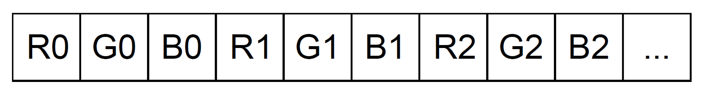
The guided image filter algorithm operates on data that is read from global memory. This data contains either different color channels or 3D-coordinates. The different dimensions of a specific pixel, however, are stored together in an interleaved fashion as is shown in Figure 6. This figure shows a 1D-array, with image data stored sequentially row-wise in memory, containing per pixel the concatenated color channels, Red (R), Green (G) and Blue (B). In order to cope with the interleaved storage of color channels, all computations are duplicated three times, once for each color channel. In this way, data can be read sequentially without discarding color channels. This leads to a SIMD-implementation in which three color channels are processed simultaneously. SIMD operations in a single work-item are realized using the OpenCL vector type. The Intel FPGA SDK for OpenCL does not support native vectorized data types containing three elements [13]. Therefore, a custom struct was defined that contains the three different channels (Listing 2). The filtering input and output images consist of real number values, while the guidance image consists of color values between 0 and 255. Therefore, two different structs were defined, respectively with 3 floats and 3 char fields.
1  __attribute__(( packed ))
2  struct guide_image
3  {
4      <type> R;
5      <type> G;
6      <type> B;
7  };
Listing 2: Structure used to vectorize image channels. Attribute “packed” creates a continuous data stream without padding.
Besides vectorizing the color channels, the mean value calculation is identical for each of its arguments. Therefore, we use vector types float4 and float2 respectively in Step 1 and 4 to compute the mean values in parallel.
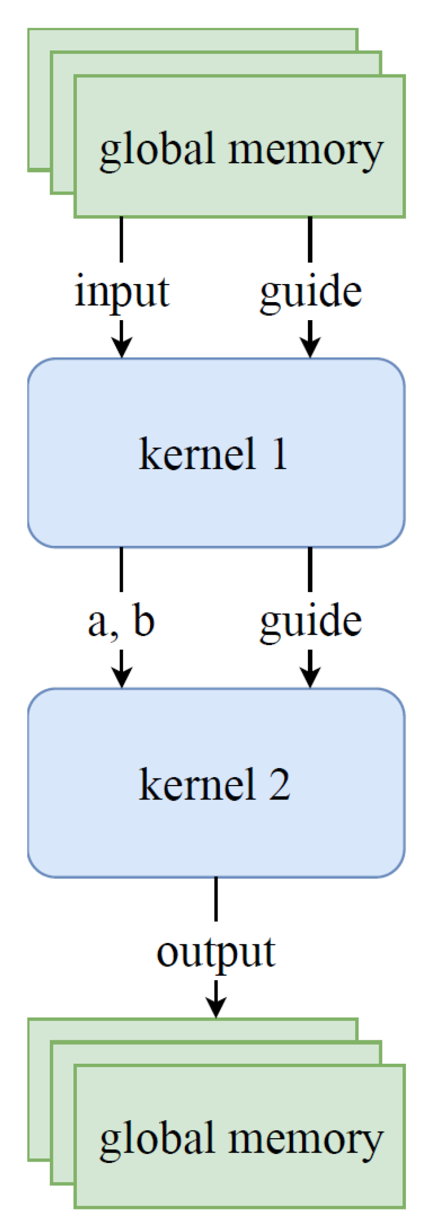
5.2.2. Kernels
In the OpenCL implementation, the guided image filter algorithm is split into two kernels, as shown in Figure 7. The first kernel calculates steps 1, 2 and 3 in Listing 1, while the second kernel calculates steps 4 and 5. Kernel 1 starts by reading the filtering image I and the guidance image G from global memory. It then slides over I and G and calculates , , and . Based on these four arrays, it then calculates the values in Step 2 and Step 3. The result of these first three steps, arrays a and b, are sent directly to the second OpenCL kernel, together with the guidance image, which is required in Step 5 of the algorithm. Kernel 2 slides over a and b, which results in arrays and . Based on and , the filtering output O is calculated and written back to global memory.
The main motivation to split the calculations into two kernels is the ease of programming. Kernel 1 contains the sliding window implementation of the four functions in Step 1 of the algorithm. In kernel 2, on the other hand, the sliding window implementation of the two functions in Step 4 is implemented. Separating these two algorithmic steps decreases the implementation complexity. Because it is possible in OpenCL to directly send data between kernels, no extra bandwidth to global memory is required for this configuration.
5.2.3. Channels
An OpenCL channel behaves as a FIFO, with a producer and a consumer. An OpenCL channel has a limited capacity, and can therefore be saturated. If this occurs, the producer stalls until data can be placed in the channel. In the OpenCL implementation of the guided image filter algorithm, arrays a and b are directly sent from kernel 0 to kernel 1 through an OpenCL channel. Moreover, as kernel 1 also needs the guidance image for its computations, kernel 0 sends this array to kernel 2 through an OpenCL channel as well. This is indicated in Listing 3. The use of channels is activated by enabling the pragma .
 1  #pragma OPENCL EXTENSION cl_altera_channels : enable
 2  channel struct struct_a_b ch_0 attribute (( depth (128) ));
 3  channel struct guide ch_1 attribute (( depth (128) ));
 4  …
 5  __kernel void guided_filter_0 ( global struct image ∗ restrict input ,
 6  global struct guide ∗ restrict guide )
 7  {
 8    …
 9    write_channel_altera (ch_0 , output_buf );
10    write_channel_altera (ch_1 , guide_buf_out );
11  }
12
13  __kernel void guided_filter_1 ( global struct image ∗ restrict output )
14  {
15    struct image_filtered input_buf = read_channel_altera ( ch_0 );
16    struct guide guide_buf = read_channel_altera ( ch_1 )
17    …
18  }
                    Listing 3: Use of OpenCL channels between two kernels.
The keyword restrict in lines 5, 6, and 13 indicates that the memory addressed by input, guide, and output does not overlap. This prevents the compiler from assuming nonexistent memory dependencies which may limit optimizations. In line 2 and line 3, the channels 0 and 1 are declared with the structs for sending the respective data values of each channel and a buffer size of 128 data elements. In line 5, kernel 1 is declared taking a pointer to the filtering input and the guide input to be read from global memory. After applying the required computations, the data, contained by variables and are sent through the channels ch 0 and ch 1 to kernel 2. Kernel 2 in line 13 reads data from the channels, performs its computations, and writes its output to the memory location pointed to by parameter output.
5.2.4. Sliding Window
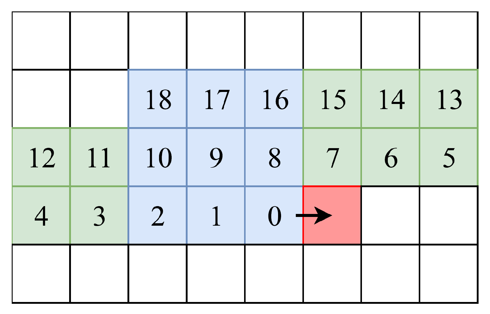
In the guided image filter algorithm, each pixel is calculated from neighboring input pixels in a window with radius r. The computational complexity is linear in the number of pixels of the image, regardless of window size site [15,16]. When the pictures are calculated sequentially, left to right, top to bottom, most pixels in the sliding window can be reused and each pixel is fetched one by one from memory. The memory usage is optimized by streaming data into a shift register which contains relevant data for the calculation of the output. The shift register is organized as a linear array of pixels in the sliding window, where w is the image width, see Figure 8. The generic code for a shift register is shown in Listing 4. In this code fragment, the data in variable shift_register is shifted over one position by looping over all indices. Then a new pixel is loaded from global memory into shift_register[0]. By spatially unrolling this loop using the pragma unroll, all shifts are executed in the same clock cycle, and a pipelined shift register is obtained. Both for-loops are fully unrolled using the pragma unroll. is then calculated by adding all values in the area and dividing this value by the size of the window. Fully unrolling the nested loops with iteration count , increases the logic resources demand. The maximum guided image filter radius r is limited by the available FPGA resources, see Section 6.1.
 1  void kernel_0 (global struct image ∗ restrict input) {
 2    int px=0;
 3    while(px < image_size) {
 4      #pragma unroll
 5      for ( int i = shift_register_size - 1; i > 0; --i) {
 6          shift_register [i] = shift_register [i - 1];
 7      }
 8      shift_register[0] = input[px];
 9      int mean = 0;
10      #pragma unroll
11      for ( int i = 0; i < 2 ∗ R + 1; i ++) {
12          #pragma unroll
13          for (int j = 0; j < 2 ∗ R + 1; j++) {
14              int value = shift_register [i ∗ IMAGE_WIDTH + j];
15              mean += value ;
16          }
17      }
18      mean = mean / ((2∗ R+1) ∗(2∗ R +1) );
19    }
20  }
                         Listing 4: Sliding window implementation.
5.2.5. Shared Virtual Memory
The shared memory architecture of the HARP platform can make use of SVM. In SVM, both the CPU and the FPGA have full access to a specially allocated memory region. Therefore, only one instance of the data is present in memory, and no explicit data copies to a separate memory region, only available for FPGA, are necessary. The use of SVM therefore significantly reduces the communication overhead when passing data to and from the OpenCL kernel. This is illustrated in the Section 6.4 of the experimental results. Interestingly, the kernel code for using shared virtual memory is unchanged. The modification is done in the host code, using the API functions clSVMAllocAltera to allocate shared memory and clSetKernelArgSVMPointerAltera to pass the arguments to the kernel.
5.2.6. Fixed-Point Calculations
One way to limit the resource usage and allow larger radius values is to use fixed-point arithmetic. The filtering input consists of floating-point variables, which results in a higher resource usage. Not only the number of DSPs will increase, the overall logic usage will increase as well. We also implemented a kernel using fixed-point variables. The bit lengths of the integer and fractional parts of the fixed-point numbers can be determined based on the intensity range of the input data as well as a minimal fractional precision. For the guided image filter, determining the intensity range is quite straightforward, as the input image and the guidance image are typically stored in an 8-bit per pixel representation. However, the calculation requires intensities to be scaled and summed and to avoid numerical overflow, it is best to over-dimension the bit lengths. We performed an analysis of the output and intermediate value ranges for the example case. As a result, we used 26 bits for the integer part and 6 bits for the fractional part in the fixed-point representation. The conversion is done in line using the code depicted in Listing 5. Since the code is pipelined, there is no conversion penalty. On the other hand, the integer calculations require much less area on the FPGA. This allows the selection of a larger radius in the guided image filter.
1    int fixed_point = (int) (floating_point_input ∗ (1 << fractional_bits ));
2    …
3    float floating_point_output = ((float) fixed_point) / (1 << fractional_bits );
                      Listing 5: In-line fixed-point conversion code.
The accuracy of the fixed-point implementation is verified at three levels. First, the selection of the place of the decimal point is based on an evaluation of the intermediate results so that there is no underflow or overflow. Second, the filtered images show no visual differences and third, the fixed-point and floating-point results are compared by computing , i.e., the relative error for the L2 norm of differences between pixel values of the two images. This gives .
6. Experimental Results
6.1. Design Space Exploration
Optimizing the OpenCL program for best performance is done in two phases. In the first phase the code and data structures are optimized for parallel and pipelined execution, as is shown in Section 5.2. In the second phase, pragmas are inserted to guide the synthesis for best performance. The goal is to achieve an initiation interval of one for each loop and avoid dependencies which enlarge the critical path. This is done by inserting #pragma unroll in a typical kernel layout shown in Listing 6. The results are shown in Table 3. The first run through the compiler with no pragmas reveals that all loops are executed serially except the last one which is enrolled completely as an automatic optimization by the compiler. The report indicates that there is a memory dependency in the shift register loop at line 6 due to a read and write at the same memory location, and a data dependency in Step 12 due to a summation calculation, creating loops with respectively II = 6 and II = 48. Unrolling the inner kernel loop is not beneficial due to data dependencies in the outer loop. Therefore, both kernel loops in lines 9 and 11 are fully unrolled to create deep pipelines. Now, the kernel loops are in-lined and the shift register loops have II = 1, but the report states that the shift register loops cannot be pipelined due to memory dependencies. After enrolling all shift register loops we obtain an initiation interval II = 1 for the whole shift operation and a drastic reduction of memory use from 94% to 41%. Furthermore, all loops are fused into one while loop (line 3) with an initiation interval of one. The resource usage of the different unroll optimizations with radius are shown in Table 3. Now it is time to generate the bitstream and profile the resulting design.
 1  __kernel guided_filter(struct image ∗ I, struct guide ∗ G) {
 2     count = 0;
 3     while(count++ < image_width∗image_height) {
 4        <#pragma unroll>
 5        for all shift_registers
 6           reg[i] = reg[i - 1];
 7
 8        <#pragma unroll>
 9        for (int i = 0; i < 2 ∗ RADIUS + 1; i++) {
10           <#pragma unroll>
11           for (int j = 0; j < 2 ∗ RADIUS + 1; j++) {
12              Steps 1-3 / Steps 4-5
13           }
14        }
15     }
16  }
                       Listing 6: Places for pragmas in the kernel code.
6.2. Runtime Measurements
The implemented kernel was synthesized to filter full-HD images, with a resolution of pixels and a radius . This generates a bitstream with operating frequency 237.5 MHz. The bitstream was then executed on the HARP platform, by filtering 100 images. Two time recordings were registered. A first recording measured the execution time of the OpenCL kernel itself, without accounting for passing input parameters. A second recording measured the total execution time at the host side. This includes the FPGA execution, but also passing the input parameters and invoking the OpenCL kernel. The average execution time per image is shown in Table 4.
Since the kernel is synthesized using a frequency of 237.5 MHz, a clock cycle time of 4.21 ns is obtained. As denoted in the compilation reports, the kernel is fully pipelined and has an initiation interval equal to one. Therefore, in every clock cycle an output pixel can be calculated. This leads to a theoretical execution time equal to approximately the total number of pixels multiplied by the cycle time, which equals 8.78 ms. If this value is compared to the obtained execution time of 18.20 ms, it can be observed that the obtained execution time is higher. This can be explained using the profiling results, displayed in Table 5.
The occupancy is defined as the portion of the execution time of the kernel that a memory operation is issued. While the optimal value is an occupancy of 100%, only an occupancy of 48.6% is achieved in this kernel. Therefore, the load and read statement are only issued 48.6% of the clock cycles, which means that a read takes around 2 clock cycles. Therefore, the bandwidth is lower as well. The theoretical requested bandwidth is 12 B/4.21 ns = 2850 MB/s. However, because of the occupancy of 48.6%, only a bandwidth of 2850 MB/s × 48.6% = 1385 MB/s ≈ 1371.6 MB/s is obtained. The low bandwidth is due to the alignment of the channel structs. Both the filtering input, the guidance input and the filtering output consist of a data type that has a size that is a multiple of 3 bytes. The filtering input, for instance, has a size of 12 B and is aligned at 4 B. Therefore, 3 separate read requests are needed, which reduces the bandwidth and explains the low occupancy.
Despite the lower occupancy, the bandwidth efficiency of all I/O-operations equals 100%, meaning that all data are effectively used. This is because all three color channels are used using structs without padding and therefore no read values are discarded.
6.3. Impact of the OpenCL Cache
When the input parameters are not marked by the keyword volatile, the OpenCL compiler adds a software implemented cache. The performance of the OpenCL cache is shown in the cache hit rates of the profiling report, see Table 6. The cache hit rate for the filtering input equals 81.5 %. This can be explained by considering the size of the struct that is used, which equals 12 B, and the size of the OpenCL cache lines, which is 64 B. Data is read from memory as 64 B cache lines. If one struct element is read, the remaining 52 B of the same cache line reside in cache memory. This leads to a cache hit ratio of 52/64 = 81.5%. Moreover, as a separate cache is created for the filtering input and the guidance input, both cache reads do not interfere with each other. The same reasoning can be applied to the cache hit ratio of the guidance image input.
6.4. Impact of SVM
To evaluate the benefit of using SVM, the kernel was also implemented using memory buffers. This leads to an additional write of the filtering and the guidance input to memory buffers, and an additional read of the filtering output from the memory buffer. The average execution time for filtering one image for both the implementation with SVM and with memory buffers is listed in Table 7. As can be seen in this table, the use of memory buffers adds approximately 10 ms to the total execution time. The amount of frames/s decreases from 45 to 30 when using memory buffers.
6.5. Roofline Performance Model
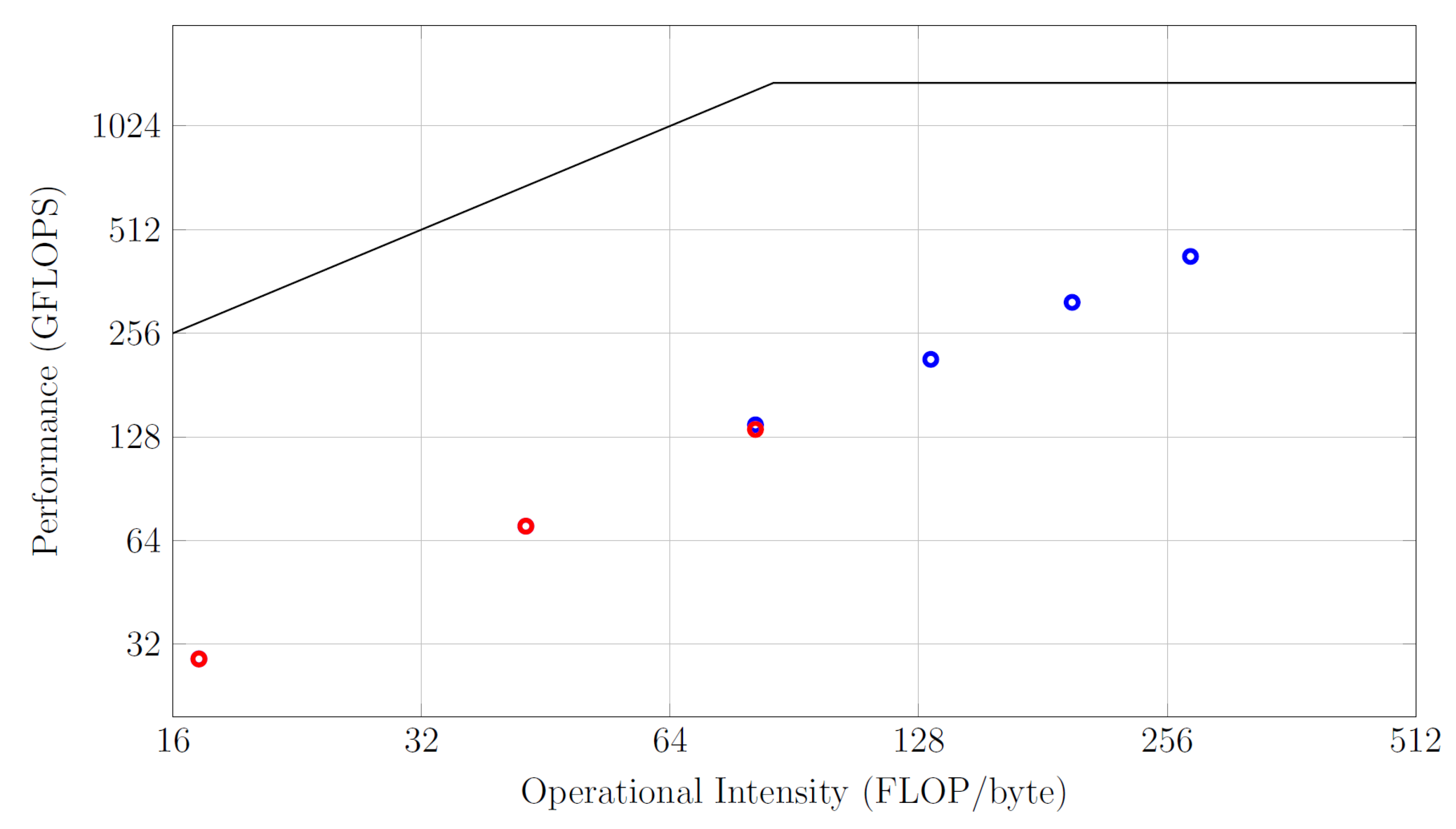
To evaluate the achieved performance, the roofline model [17] can be used. This model relates the operational intensity to the achieved performance. In the guided image filter, the operational intensity, however, depends on the value of radius. A larger radius results in more operations to be performed for an equal amount of data that is read, and therefore a higher operational intensity. The number of operations per pixel is given by , e.g., and . The maximum radius for a floating-point implementation of the guided image filter algorithm is . For higher values, the synthesized hardware does not fit in the FPGA anymore. Therefore, a fixed-point implementation was used, which could go up to a radius . Both the floating-point and fixed-point implementations of the guided image filter were executed for the possible values for radius. This results in the measured performance depicted in Figure 9. In this figure, the performance of the kernels for the different operational intensities is shown. The fixed-point kernel performance is indicated by the blue dots, while the floating-point kernel performance measurements are shown in red. Moreover, the roofline model of the HARP platform is shown as well. As peak-memory bandwidth, the bandwidth of 16 GB/s is used. The peak floating-point performance of the Arria 10 FPGA equals 1366 GFLOPS. This should be interpreted in the following way. The Arria 10 FPGA consists of 1518 DSPs. Each of these DSPs can perform 2FLOP/clock cycle, which results in 3036 FLOP/clock cycle for all DSPs. At a rate of 450 MHz, this results in 3036 FLOP/clock cycle × 450 MHz = 1366 GFLOPS [18].
Please note that for the fixed-point kernel, the performance should be expressed in OPerations per Second (OPS), instead of FLOPS. As can be seen in Figure 9, the implementation definitely benefits from using the fixed-point implementation. While the maximum achievable performance of the floating-point kernel is 135 GFLOPS, the fixed-point kernel achieves a top performance of 430 GOPS. For radii that both the floating-point and the fixed-point kernel can implement, on the other hand, no significant difference in performance can be observed. In this case, using the floating-point implementation is advantageous due to the specific issues of the fixed-point implementation, such as under- and overflow. Furthermore, it can be seen in Figure 9 that for larger operational intensities, a higher performance is obtained. Therefore, the larger computational demands do not hamper the performance and the kernel is only limited by the achieved bandwidth. It can, however, be seen that the maximum performance of the floating-point kernel, 135 GFLOPS, is smaller than the compute limit of 1366 GFLOPS. This can be explained as follows. The number of floating-point operations for radius 3 is 1218 per cycle. The clock frequency for the design is 237.5 MHz. The occupancy of the requested bandwidth is 48.6%. This gives a performance estimation of operations per second or 140.6 GFLOPS, which is 4% above the measured value.
Up until this point, one pixel, consisting of three different color channels, was processed in parallel. It is, however, possible to process two or four pixels simultaneously, resulting in either six or 12 parallel calculations. The execution times for these different kernels are listed in Table 8. The maximum performance is obtained when processing 2 pixels simultaneously, in which a minimum execution time of 9.45 ms is obtained. However, considering the overhead by setting the input parameters and invoking the kernel, a total execution time of 13.45 ms is achieved. This results in a maximum frame rate of 74 frames/s.
7. Related Work
Since the publication of the guided image filter [15], its importance has been recognized as a fast, efficient filter to perform edge-preserving smoothing. Numerous publications have been focusing on respectively modifying the algorithm for faster execution using limited resources [19], implementation in hardware using VLSI prototypes [6,20,21], programming the algorithm in domain specific languages [22], or synthesizing the filter code for FPGAs using OpenCL [23,24,25]. Image filtering is also an active research topic using GPUs [26,27].
Kareem et al. [19] propose optimizations with respect to the memory requirements and the computation speed of the algorithm. In order to limit the memory consumption, Step 4 of Algorithm 1 is removed and in Step 5, the values of a and b are used directly from Step 3. Furthermore, the division is replaced by a shift of log2 steps. This results in a faster calculation with less memory and acceptable accuracy according to the authors. Finally, the authors used a striping method in which the image is divided into vertical stripes and the computation is done successively on each stripe. In this way the on-chip memory cost is significantly reduced. Kao et al. [6] present a VLSI architecture for the guided filter realizing full-HD video at 30 frames per second. Accessing the image data from off-chip memory requires a huge bandwidth. This is solved by creating a double integral image architecture. Furthermore, fixed-point arithmetic is used to alleviate the sharply rising on-chip memory when using floating-point operations. The chip achieves a frame rate of 30 frames per second at an operating frequency of 100 MHz. Ttofis et al. [21] present the design and implementation of a stereo matching system incorporating two guided image filters. They tested their prototype on an FPGA and obtained a speed of 60 frames per second on 720p HD video. Besides the design of hardware cores, many authors have analyzed programming languages and techniques to program the configurable hardware, e.g., FPGAs. Ishikawa et al. [22] extended the domain specific language Halide with an FPGA extension Genesis. Genesis is a source the source compiler translating Halide code into Vivado C/C++. This code is then transformed into a bitstream for a SPG using the Vivado HLS compiler. Simulation results were obtained for a 512×512 image on a Xilinx ZedBoard. Most high-level system support is available for the language OpenCL, which is provided both by Xilinx and Intel. Wang et al. [23] describe the internal architecture of the compiler and present four optimizations, use of local memory, loop unrolling, kernel vectorization, and pipelining. They also present four performance metrics which the programmers can use to evaluate the design. The metrics are global memory potential, computing potential, pipeline balance potential, and inter-thread pipelining potential. Unfortunately, these metrics cannot easily be derived from compiler or monitoring reports. In contrast, we use the initiation interval and memory occupancy as supported metrics to optimize the design. In Momeni et al. [24] the OpenCL Pipe semantic is evaluated. This semantic compiler construct generates automatic first in first out channels between consecutive kernels. Momeni found an increase of 2.8 times the throughput with respect to a non-pipelined execution. We use pipes to connect the two kernels in our guided filter. The work of Zohouri et al. [25] is closely related to our work. Zohouri presents a spatial and temporal blocking algorithm to perform stencil computations on large images. He uses temporal locality to reuse the data in the shift registers as is done in this paper. He also uses spatial blocking to organize parallel computations with physically different processing engines. In our case we use only temporal blocking due to the limited resources in the FPGA. Furthermore, spatial blocking requires much more bandwidth to feed the different processing engines. Besides the general concept, we use pragmas and options of the OpenCL compiler to alleviate problems which were manually solved in Zohouri’s paper. For example, in [25] the loops are coalesced and translated into nested while statements to avoid critical loop overhead at the boundaries of an iteration. In our solution, we used the pragma “unroll” to let the compiler unroll the loops and create deep pipelines, which are resulting in an initiation interval of 1. Also, in [25] the external memory accesses are padded, because they are not aligned to a 512-bit buswidth. This was a solved in our application by using the attribute “packed”, which optimizes the bandwidth and creates no overhead. The details about the complexity of the temporal/spatial code were not given. However, our performance is of the same order of magnitude than the examples given in [25]. Finally, many image filters have ample parallelism for an excellent performance on the GPU. In [26] parameterized operators run at 5.88 ms for a 1080p image and real-time dehazing is done at 38 frames per second in [27]. While difficult to compare, these results are in line with results obtained from using OpenCL on the HARP system.
8. Conclusions
The goal of this research was to evaluate the OpenCL as an HLS language for the implementation of a guided image filter on the HARP platform. We have performed this evaluation by using synthetic benchmarks to measure the maximum bandwidth, the influence of the OpenCL cache as well as SVM, and then using the results as guidelines to implement and optimize the guided image filter. Our implementation of the guided image filter processes RGB images of pixels at 74 frames/s.
Based on our findings it can be stated that the HARP platform offers several architectural structures that benefit the implementation of applications such as the guided image filter. Furthermore, OpenCL for HARP allows the tapping of these benefits and the use of specific optimizations to exploit the architectural structures of HARP that improve the implementation. The main advantages are the shared memory and the high bandwidth. HARP uses shared DRAM memory for the CPU and the FPGA. As this shared memory approach is supported by shared virtual memory in OpenCL, this can be fully exploited. Furthermore, a high CPU-FPGA bandwidth is available to OpenCL developers. Besides the HARP platform, the OpenCL compiler offers performance enhancing advantages. A highly effective feature is the implementation of the OpenCL cache. This cache can provide data at a high data rate, and reduces the amount of memory requests. The OpenCL profiler is useful to evaluate the OpenCL kernel. Performance characteristics are visualized in an uncomplicated way, which allows an easy performance analysis.
Author Contributions
Conceptualization, E.H.D. and B.G.; Methodology, T.F., E.H.D. and B.G.; Software T.F.; Validation T.F. and E.H.D.; Formal Analysis, T.F.; Investigation, T.F., E.H.D. and B.G., Writing—Original Draft Preparation E.H.D., Writing—Review and Editing E.H.D., T.F. and B.G., Supervision E.H.D. and B.G.
Funding
This research received no external funding.
Acknowledgments
We appreciate the useful comments and feedback from the anonymous reviewers. We thank Intel for the donation of the development tools and hardware. The presented HARP-2 results were obtained on resources hosted at the Paderborn Center for Parallel Computing (PC2) in the Intel Hardware Accelerator Research Program (HARP2).
Conflicts of Interest
The authors declare no conflicts of interest.
References
- Dennard, R.H.; Gaensslen, F.H.; Rideout, V.L.; Bassous, E.; LeBlanc, A.R. Design of ion-implanted MOSFET’s with very small physical dimensions. IEEE J. Solid-State Circuits 1974, 9, 256–268. [Google Scholar] [CrossRef]
- Hennessy, J.L.; Patterson, D.A. A new golden age for computer architecture. Commun. ACM 2019, 62, 48–60. [Google Scholar] [CrossRef] [Green Version]
- Oliver, N.; Sharma, R.R.; Chang, S.; Chitlur, B.; Garcia, E.; Grecco, J.; Grier, A.; Ijih, N.; Liu, Y.; Marolia, P.; et al. A Reconfigurable Computing System Based on a Cache-Coherent Fabric. In Proceedings of the 2011 International Conference on Reconfigurable Computing and FPGAs (ReConFig), Cancun, Mexico, 30 November–2 December 2011; pp. 80–85. [Google Scholar]
- Rahamneh, S.; Sawalha, L. An OpenCL-Based Acceleration for Canny Algorithm Using a Heterogeneous CPU-FPGA Platform. In Proceedings of the 2019 IEEE 27th Annual International Symposium on Field-Programmable Custom Computing Machines (FCCM), San Diego, CA, USA, 28 April–1 May 2019; p. 322. [Google Scholar] [CrossRef]
- Gupta, P. Accelerating Datacenter Workloads, Keynote at FPL 2016; Lausanne, Switzerland, 2016.
- Kao, C.; Lai, J.; Chien, S. VLSI Architecture Design of Guided Filter for 30 Frames/s Full-HD Video. IEEE Trans. Circuits Syst. Video Technol. 2014, 24, 513–524. [Google Scholar] [CrossRef]
- Flynn, M.J.; Rudd, K.W. Parallel Architectures. ACM Comput. Surv. 1996, 28, 67–70. [Google Scholar] [CrossRef]
- Stitt, G.; Gupta, A.; Emas, M.N.; Wilson, D.; Baylis, A. Scalable Window Generation for the Intel Broadwell+Arria 10 and High-Bandwidth FPGA Systems. In Proceedings of the 2018 ACM/SIGDA International Symposium on Field-Programmable Gate Arrays (FPGA ’18), Monterey, CA, USA, 25–27 February 2018; ACM Press: New York, NY, USA, 2018; pp. 173–182. [Google Scholar] [CrossRef]
- Intel. An Introduction to the Intel QuickPath Interconnect; Technical report 320412–001US; Intel: Santa Clara, CA, USA, January 2009. [Google Scholar]
- Intel. Acceleration Stack for Intel Xeon CPU with FPGAs Core Cache Interface (CCI-P) Reference Manual MNL-1092; Technical report; Intel: Santa Clara, CA, USA, 2018. [Google Scholar]
- Khronos. The OpenCL Specification 1.2. 2012. Available online: https://www.khronos.org/registry/OpenCL/specs/opencl-1.2.pdf (accessed on 27 July 2019).
- Munshi, A. The OpenCL specification. In Proceedings of the 2009 IEEE Hot Chips 21 Symposium (HCS), Stanford, CA, USA, 23–25 August 2009; pp. 1–314. [Google Scholar] [CrossRef]
- Intel. FPGA SDK for OpenCL™ Programming Guide; Technical report UG-OCL002; Intel: Santa Clara, CA, USA, 2017. [Google Scholar]
- Intel. FPGA SDK for OpenCL™ Pro Best Practices Guide UG-OCL003; Technical report; Intel: Santa Clara, CA, USA, 2018. [Google Scholar]
- He, K.; Sun, J.; Tang, X. Guided Image Filtering. IEEE Trans. Pattern Anal. Mach. Intell. 2013, 35, 1397–1409. [Google Scholar] [CrossRef]
- Stacey, A.; Maddern, W.; Singh, S. Fast Light Field Disparity Estimation via a Parallel Filtered Cost Volume Approach. In Computer Vision—ACCV 2018; Jawahar, C.V., Li, H., Mori, G., Schindler, K., Eds.; Lecture Notes in Computer Science; Springer International Publishing: Cham, Switzerland, 2019; pp. 256–268. [Google Scholar]
- Williams, S.; Waterman, A.; Patterson, D. Roofline: An insightful visual performance model for multicore architectures. Commun. ACM 2009, 52, 65–76. [Google Scholar] [CrossRef]
- Parker, M. Understanding Peak Floating-Point Performance Claims; White Paper WP-01222-1.1; Intel: Santa Clara, CA, USA, February 2017. [Google Scholar]
- Kareem, P.; Khan, A.; Kyung, C. Memory efficient self guided image filtering. In Proceedings of the 2017 International SoC Design Conference (ISOCC), Seoul, Korea, 5–8 November 2017; pp. 308–309. [Google Scholar] [CrossRef]
- Chang, C.; Huang, I.; Lin, M.; Kuang, S. Design and implementation of a low-cost guided image filter for underwater image enhancement. In Proceedings of the 2017 IEEE Conference on Dependable and Secure Computing, Taipei, Taiwan, 7–10 August 2017; pp. 296–299. [Google Scholar] [CrossRef]
- Ttofis, C.; Kyrkou, C.; Theocharides, T. A Low-Cost Real-Time Embedded Stereo Vision System for Accurate Disparity Estimation Based on Guided Image Filtering. IEEE Trans. Comput. 2016, 65, 2678–2693. [Google Scholar] [CrossRef]
- Ishikawa, A.; Fukushima, N.; Maruoka, A.; Iizuka, T. Halide and GENESIS for Generating Domain-Specific Architecture of Guided Image Filtering. In Proceedings of the 2019 IEEE International Symposium on Circuits and Systems (ISCAS), Sapporo, Japan, 26–29 May 2019; pp. 1–5. [Google Scholar] [CrossRef]
- Wang, Z.; He, B.; Zhang, W.; Jiang, S. A performance analysis framework for optimizing OpenCL applications on FPGAs. In Proceedings of the 2016 IEEE International Symposium on High Performance Computer Architecture (HPCA), Barcelona, Spain, 12–16 March 2016; pp. 114–125. [Google Scholar] [CrossRef]
- Momeni, A.; Tabkhi, H.; Ukidave, Y.; Schirner, G.; Kaeli, D. Exploring the Efficiency of the OpenCL Pipe Semantic on an FPGA. ACM SIGARCH Comput. Archit. News 2016, 43, 52–57. [Google Scholar] [CrossRef]
- Zohouri, H.R.; Podobas, A.; Matsuoka, S. Combined Spatial and Temporal Blocking for High-Performance Stencil Computation on FPGAs Using OpenCL. In Proceedings of the 2018 ACM/SIGDA International Symposium on Field-Programmable Gate Arrays (FPGA ’18), Monterey, CA, USA, 25–27 February 2018; ACM Press: New York, NY, USA, 2018; pp. 153–162. [Google Scholar] [CrossRef] [Green Version]
- Fan, Q.; Chen, D.; Yuan, L.; Hua, G.; Yu, N.; Chen, B. A General Decoupled Learning Framework for Parameterized Image Operators. IEEE Trans. Pattern Anal. Mach. Intell. 2019. [Google Scholar] [CrossRef] [PubMed]
- Wu, X.; Wang, R.; Li, Y.; Liu, K. Parallel Computing Implementation for Real-Time Image Dehazing Based on Dark Channel. In Proceedings of the 2018 IEEE 20th International Conference on High Performance Computing and Communications; IEEE 16th International Conference on Smart City; IEEE 4th International Conference on Data Science and Systems (HPCC/SmartCity/DSS), Exeter, UK, 28–30 June 2018; pp. 1–5. [Google Scholar] [CrossRef]
Figure 1.
HARPv2 heterogeneous architecture, consisting of an Intel Xeon CPU and Arria 10 FPGA with QPI and PCIe interconnects. The QPI and PCIe channels are respectively 16 and 8 bit wide.
Figure 1.
HARPv2 heterogeneous architecture, consisting of an Intel Xeon CPU and Arria 10 FPGA with QPI and PCIe interconnects. The QPI and PCIe channels are respectively 16 and 8 bit wide.

Figure 2.
(a) Single work-item kernel adding 2 vectors a and b. (b) NDRange kernel for vector addition. The n-dimensional range is given in the call in the host computer.
Figure 2.
(a) Single work-item kernel adding 2 vectors a and b. (b) NDRange kernel for vector addition. The n-dimensional range is given in the call in the host computer.

Figure 3.
OpenCL and C programming steps to generate an FPGA configuration bitstream.

Figure 4.
Bandwidth for various buffer sizes and data widths.

Figure 5.
Bandwidth of reading src when executing kernel cache read for ulong16 pointer types. The bandwidth for both the kernel with (blue) and without (red) the volatile keyword is displayed.
Figure 5.
Bandwidth of reading src when executing kernel cache read for ulong16 pointer types. The bandwidth for both the kernel with (blue) and without (red) the volatile keyword is displayed.

Figure 6.
Stream of image data.

Figure 7.
Kernel 1 computes the first three steps in the guided image filter algorithm, while kernel 2 computes the last two steps.
Figure 7.
Kernel 1 computes the first three steps in the guided image filter algorithm, while kernel 2 computes the last two steps.

Figure 8.
Shift register of an image with and . The sliding window for pixel 9 is indicated in blue. In the next clock cycle, the red pixel will be loaded in the shift register in local memory.
Figure 8.
Shift register of an image with and . The sliding window for pixel 9 is indicated in blue. In the next clock cycle, the red pixel will be loaded in the shift register in local memory.

Figure 9.
Roofline model HARP platform. The red dots indicate the performance of the floating-point kernel for different values of radius while the blue dots indicate the performance of the fixed-point implementation for radii .
Figure 9.
Roofline model HARP platform. The red dots indicate the performance of the floating-point kernel for different values of radius while the blue dots indicate the performance of the fixed-point implementation for radii .


Table 1.
QPI and PCIe characteristics.
| QPI | PCIe Gen.3×8 | |
|---|---|---|
| width | 16 bits | 8 bits |
| max #transfers per second | 6.4 GT/s | 8 GT/s |
| maximum raw unidirectional bandwidth | 12.8 GB/s | 7.88 GB/s |
Table 2.
FLOPs calculation for a full-HD RGB image with radii and .
| Step | FLOPS | Radius = 3 | Radius = 6 |
|---|---|---|---|
| 1 | 294 | 1014 | |
| 2 | 6 | 6 | 6 |
| 3 | 5 | 5 | 5 |
| 4 | 98 | 338 | |
| 5 | 1 | 1 | 1 |
| Total/px | 32 + 32r + 22 | 406 | 1366 |
| Total/image | 3(32 + 32r + 22)*1920*1080 |
Table 3.
Resource usage and maximum initiation interval (II) for various loop unroll pragmas in the code.
Table 3.
Resource usage and maximum initiation interval (II) for various loop unroll pragmas in the code.
| Resource | No Pragmas | Inner Loops | Both Loops | Shift Registers |
|---|---|---|---|---|
| Logic | 61% | 65% | 93% | 90% |
| LUT | 27% | 29% | 40% | 39% |
| RAM | 46% | 49% | 94% | 41% |
| DSP | 20% | 28% | 87% | 87% |
| II | 48 | 48 | 1 | 1 |
Table 4.
Execution times when executing the sliding window implementation of the guided filter on the HARP platform.
Table 4.
Execution times when executing the sliding window implementation of the guided filter on the HARP platform.
| Profile | Execution Time | GOPS | Frames/s |
|---|---|---|---|
| Kernel Execution | 18.20 ms | 139 | 54 |
| Total Execution | 22.06 ms | 114 | 45 |
Table 5.
Profiling results when executing the sliding window implementation of the guided image filter algorithm.
Table 5.
Profiling results when executing the sliding window implementation of the guided image filter algorithm.
| Memory Operation | Occupancy | Bandwidth | Efficiency |
|---|---|---|---|
| Filtering Input | 48.6% | 1371.6 MB/s | 100% |
| Guidance Input | 48.6% | 343.0 MB/s | 100% |
| Filtering Output | 48.5% | 1459.9 MB/s | 100% |
Table 6.
Cache hit rates in the OpenCL generated cache.
| Memory Operation | OpenCL Cache Hit Rate |
|---|---|
| Filtering input | 81.5% |
| Guidance Input | 95.4% |
Table 7.
Execution times of the guided filter on HARP with and without shared virtual memory.
| Profile | Execution Time | GOPS | Frames/s |
|---|---|---|---|
| SVM | 22.06 ms | 114 | 45 |
| Memory Buffer | 32.72 ms | 77 | 30 |
Table 8.
Kernel execution times when processing a different number of pixels in parallel.
| #Pixels in Parallel | Kernel Execution Time |
|---|---|
| 1 | 18.20 ms |
| 2 | 9.45 ms |
| 4 | 20.00 ms |
© 2019 by the authors. Licensee MDPI, Basel, Switzerland. This article is an open access article distributed under the terms and conditions of the Creative Commons Attribution (CC BY) license (http://creativecommons.org/licenses/by/4.0/).
Share and Cite
MDPI and ACS Style
Faict, T.; D’Hollander, E.H.; Goossens, B. Mapping a Guided Image Filter on the HARP Reconfigurable Architecture Using OpenCL. Algorithms 2019, 12, 149. https://doi.org/10.3390/a12080149
AMA Style
Faict T, D’Hollander EH, Goossens B. Mapping a Guided Image Filter on the HARP Reconfigurable Architecture Using OpenCL. Algorithms. 2019; 12(8):149. https://doi.org/10.3390/a12080149
Chicago/Turabian StyleFaict, Thomas, Erik H. D’Hollander, and Bart Goossens. 2019. "Mapping a Guided Image Filter on the HARP Reconfigurable Architecture Using OpenCL" Algorithms 12, no. 8: 149. https://doi.org/10.3390/a12080149
Note that from the first issue of 2016, this journal uses article numbers instead of page numbers. See further details here.