

Abstract
Zinc-oxide (ZnO) nanorod arrays were successfully prepared by using dual sonication sol–gel process. Field emission scanning electron microscopy revealed that the nanorods exhibited a hexagonal structure with a flat-end facet. The nanorods displayed similar surface morphologies and grew uniformly on the seed layer substrate, with the average diameter slightly increasing to the range of 65 to 80 nm after being immersed for varying growth times. Interestingly, thickness measurements indicated that the thicknesses of the samples increased as the growth time was extended. In addition, the X-ray diffraction spectra indicated that the prepared ZnO nanorods with a hexagonal wurtzite structure grew preferentially along the c-axis. Therefore, we can conclude that the diameter, length, and orientation of the ZnO nanorod arrays along the c-axis are controllable by adjusting the growth time, motivating us to further explore the growth mechanisms of ZnO nanorods.
Export citation and abstract BibTeX RIS
1. Introduction
ZnO is an n-type semiconductor with a direct band gap energy of 3.37 eV at room temperature and free-exciton binding energy of 60 meV; it exhibits excellent chemical and thermal stability, non-toxicity, good piezoelectric properties, and bio-compatibility.1,2) The properties of ZnO are strongly dependent on crystallinity, crystallographic orientation, crystallite size, and morphology. Recently, ZnO thin films gained significant interest because of their potential applications in engineering, such as blue and ultraviolet (UV) light emitters,3) solar cell windows,4) energy efficient windows, electrochromic displays (ECDs), liquid crystal displays, sensors,5) and optoelectronic devices, among others.
The synthesis of ZnO nanostructures in the form of nanorods, nanotubes, nanobelts, nanorings, nanoflowers, nanosheets, and nanowires has received extensive attention because of the increased importance of one-dimensional (1D) structures for electronic transport and optical excitations. Many efforts were made to synthesize 1D ZnO nanostructures, particularly vertically aligned nanorod arrays because of their appealing characteristics for various applications in existing and emerging electronic and optoelectronic industries. 1D ZnO nanostructures were considered important materials in dye sensitized solar cells (DSSCs) because of their unique optical and electronic properties. For example, ZnO in the form of 1D nanorod arrays can be used as active layers and electrodes in DSSCs. These structures show improved optical absorption properties and excellent crystallinity that enhances electronic transportation. Furthermore, the electron transport is reported to be tens to hundreds of times faster in nanorod array electrodes compared with nanoparticle structure electrodes in DSSCs.
Various techniques were employed to produce vertically aligned ZnO nanorods or nanowire arrays, including pulsed laser deposition (PLD), vapor–liquid–solid (VLS) growth,6) electrochemical deposition (ECD),7) chemical vapor deposition (CVD),8) and electrochemical deposition (ED). However, all of these processes require expensive and sophisticated equipment and rigorous conditions, such as relatively high temperature, single-crystalline substrate, chemical vapor transport, and condensation system. All these requirements limit the industrial application of these techniques, particularly for large-scale production. Solution immersion technique is especially appealing because of its low-temperature synthesis, and the simplicity of its experimental setup is more convenient and economical for large-scale preparation of well-ordered ZnO nanorod arrays.9) Furthermore, the growth of nanorods can be controlled under solution immersion method by optimizing the solution and deposition parameters. The controllable growth of aligned ZnO nanorods is very important to achieve the desired level of functionality that satisfies application requirements. The purpose of this work is to study the effect of immersion growth time on the growth of ZnO nanorods by novel dual sonication sol–gel process. Thus, the aim of this study is to determine the optimal conditions to grow perfectly aligned and uniform ZnO nanorods and provide the basis to achieve better controlled and large-scale synthesis of ZnO nanorods.
2. Experimental methods
In this experiment, ZnO nanorod arrays were grown on a seed layer-coated glass substrate using novel dual sonication sol–gel process [Intellectual Property Corporation of Malaysia (MyIPO) — Notification No. CRLY00001855]. The seed layer, which consists of aluminium doped ZnO (AZO) nanoparticles, was deposited on the glass substrates by sol–gel dip coating technique. The details on the AZO seed-layer preparation are described elsewhere.10) ZnO nanorod arrays were grown using aqueous solutions of 0.1 M zinc nitrate hexahydrate Zn(NO3)2  6H2O, 0.1 M hexamethylenetetramine C6H12N4 (HMT), and 1 mM aluminium nitrate nonahydrate Al(NO3)3 9H2O. The reagents were dissolved in a beaker filled with distilled water as a solvent under ultrasonic irradiation using ultrasonic water bath (Hwasin Technology Powersonic 405, 40 kHz). The solution was stirred and aged at room temperature. The resulting solution was poured into a 100 ml container (Schott bottle). The AZO seed layer-coated glass substrates were placed at the bottom of the container. The vessels were sealed and transferred to a water bath instrument for the hydrothermal process. During this process, the temperature was maintained at 95 °C. The immersion time was varied between 5 and 30 min. After being immersed, the vessels were removed from the hot water bath, and the samples were immediately taken out from the containers. The nanostructures deposited on the substrates were rinsed thoroughly with distilled water and annealed in a furnace at 500 °C for 1 h. Selecting zinc nitrate rather than zinc acetate results in the more feasible nucleation of ZnO nanostructures. This phenomenon occurs because precipitation more likely occurs in a solution containing nitrate salts.11) The corresponding process is shown in Fig. 1. The thin film crystal structure properties and phases of ZnO nanorod arrays were investigated using a PANalytical X'Pert3 Powder X-ray diffractometer in a standard θ–2θ Bragg–Brentano geometry configuration with a monochromatic Cu Kα (λ = 0.154 nm) radiation. Scan pattern data were collected between 30 and 55° with step lengths of 0.02°. The morphology and topography of nanorod films were characterized using a field emission scanning electron microscope (FESEM; JEOL JSM 7600F) with an electron beam energy acceleration voltage of 4 and 5 kV. The film thickness was measured using a KLA Tencor P-6 profilometer. The sample transmission spectra were determined using a Varian Cary 5000 UV–vis–NIR spectrophotometer between 350 and 800 nm at room temperature in air with a data interval of 1 nm.

Fig. 1. Schematic diagram of ZnO nanorod array preparation procedure at various growth times.
Download figure:
Standard image High-resolution image3. Results and discussion
Growth time is one of prominent processes that affect the structural and crystal orientation properties of ZnO thin film. The crystal structure of the ZnO nanorod arrays thin films was characterized using X-ray diffraction (XRD) measurements. Figure 2 shows the XRD patterns of ZnO nanorod array thin films fabricated for various growth times and the ZnO-based seed layer with an average crystallite size of approximately 20 nm. All the samples exhibit diffraction peaks, which can be indexed as the hexagonal phase ZnO with a wurtzite structure (JCPDS 36-1451). The adhesion of the ZnO nanorod array thin films to the glass substrate was examined by an ordinary tape peel test using 3M Scotch Tape™. None of the films deposited on glass substrates were removed, indicating the strong adherence of the films to the glass substrates. The XRD pattern indicates that mostly four peaks appear at 2θ ∼ 31.7, 34.4, 36.2, and 47.5°, which correspond to the (100), (002), (101), and (102) crystallographic planes of ZnO, respectively. The XRD peaks of the seed layer are relatively weak compared with that of the prepared ZnO nanorods. Evidently, all of the XRD patterns exhibit the strongest (002) orientation peak centered at 34.4°, yielding the highest intensity compared with other peaks. The intensity of the (002) peak improves as the ZnO nanorod arrays were grown at longer growth times. This result suggests that the growth of ZnO nanorod arrays intensifies with longer growth times, which produces longer nanorods on the seed layer-coated glass substrate. These results verify that these ZnO nanorod thin films possess the highly preferred orientation along the c-axis or perpendicular to the substrate. Meanwhile, other orientation peaks indicate very weak intensities which may be attributed to the imperfect ZnO nanorod array alignment on the substrate.

Fig. 2. XRD patterns of ZnO nanorod arrays prepared at various growth times.
Download figure:
Standard image High-resolution imageThe morphology and cross-sectional image of the AZO seeded layer thin films for the growth of ZnO nanorods are shown in Figs. 3(a) and 3(b), as previously reported.10) The AZO seeded layer possesses a crystallite size of approximately 23 nm with a thickness of 135 nm. Figures 3(c)–3(h) illustrate the top and cross-sectional view of the FESEM images of ZnO nanorod array thin films deposited at various growth times. In this experiment, the growth time was between 5 to 30 min. The images clearly indicate that large-scale and well-oriented ZnO nanorod array thin films were uniformly and densely deposited on the substrates. The nanorods exhibit a hexagonal shape structure with a flat-top facet. Evidently, the surface morphology of ZnO nanorod thin films immersed for 5 min show aggregated hexagonal grains and more compact structure than other thin films, as shown in Fig. 3(c). This outcome may be attributed to the higher saturation level of Zn2+ and OH− ions, which exceeds supersaturation. Thus, ZnO nuclei are formed on the surface of the seeded layer thin films. Additionally, the growth of the aligned ZnO nanorod arrays is initiated because of nucleation and crystallization growth as temperature increased (above 85 °C).12) However, as growth time increased, the film became visibly composed of a large bundle of ZnO nanorods. Most nanorods do not fuse together, resulting in the formation of many unfilled inter-columnar volumes between nanorods. The average diameters of the nanorods in all the samples only exhibit a slight increase ranging from 65 to 80 nm, whereas the morphology remained the same as growth time increased, as observed in Figs. 3(d)–3(g). The cross-sectional image of the nanorods prepared for 15 min are shown in Fig. 3(h). To investigate growth behavior, the thickness of the nanorod array thin films was measured at different growth times, as presented in Fig. 4. The seed layer used for this experiment has an average thickness of 135 nm. After immersing the ZnO seed-layer in the precursor solution for 5 min, the thickness of the film increased to 236 nm. The samples immersed for 10, 15, 20, and 30 min growth times exhibited average thickness values of 389, 574, 632, and 659 nm, respectively.
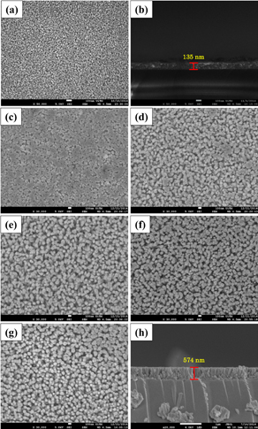
Fig. 3. FESEM images of (a) AZO seeded layer thin films and (b) cross-sectional image of AZO seeded layer thin films. ZnO nanorod arrays prepared on AZO seeded layer thin films at various growth times (c) 5, (d) 10, (e) 15, (f) 20, and (g) 30 min. Cross-sectional image of ZnO nanorod arrays growth for (h) 15 min.
Download figure:
Standard image High-resolution image
Fig. 4. Plots of ZnO nanorod arrays thickness (with 135 nm seeded layer) versus growth time.
Download figure:
Standard image High-resolution imageThickness increased with growth time. The thickness variation obtained by the surface profiler is presented in Table I. The lengths of the nanorods increased without significantly affecting the nanorod diameter after being exposed to longer growth time. This result indicates that the thickness of the nanorods along the c-axis can be obtained by controlling growth time in our novel dual sonication sol–gel process. However, the thickness of the ZnO nanorod tends to saturate above 15 min, which may be attributed to the decrement in Zn2+ and OH− ions with increased growth time. Some tilted nanorods were also observed after a longer growth time, which was confirmed by XRD analysis. This finding indicates that the growth of the ZnO nanorod arrays occurs primarily along the c-axis.
Table I. Thicknesses, average transmittance, and porosity of ZnO nanorod array thin films deposited at various growth times.
| Sample | Growth time, t (min) | Length of nanorod, t (nm) | Average diameter of nanorod, d (nm) | Aspect ratio | Average transmittance, T (%) | Porosity (%) |
|---|---|---|---|---|---|---|
| 1 | Seed layer | 135 | — | — | 96.65 | — |
| 2 | 5 | 236 | 66 | 3.5 | 96.37 | — |
| 3 | 10 | 389 | 70 | 5.5 | 95.07 | 57.70 |
| 4 | 15 | 574 | 73 | 7.8 | 94.58 | 53.62 |
| 5 | 20 | 632 | 75 | 8.4 | 92.53 | 42.19 |
| 6 | 30 | 659 | 77 | 8.5 | 92.30 | 41.17 |
Several significant variables, such as the morphology of the seed layer, growth temperature, pH, concentration of solution, and volume of solution, were reported to affect the growth characteristics of the lengths and average diameters of ZnO nanorod arrays. The presence of the ZnO nanocrystal seed layer during the initial stage of the process is crucial because this seed layer provides heterogeneous nucleation sites for ZnO formation. The shape of ZnO nanostructures depends on the growth habit of the hexagonal wurzite structure of ZnO. ZnO consists of polar and non-polar faces. ZnO is a polar crystal. Thus, each Zn atom is tetrahedrally coordinated to four O atoms, and vice versa. The alternating arrangement of Zn2+ and O2− ions along the c-axis yields either positive or negative charges depending on the terminating ions. The growth of the ZnO nanorod arrays was thought to occur through a self-assembly mechanism during the hydrothermal process. Based on these results, a possible growth mechanism of ZnO nanorod array thin film prepared at various growth times using dual sonication sol–gel process is proposed. A schematic illustration of the possible formation mechanism of the ZnO nanorods is depicted in Fig. 5. The formation of ZnO nanorod arrays along the c-axis may be caused by the applied sonication process that disperses and mixes the precursor and the stabilizer very well. The sonication process enhances the crushing rate of the agglomerated zinc nitrate and HMT particles that intensify the physical and chemical reaction activity in the solution. In our proposed growth mechanism, Zn2+ and OH− were produced by the hydrolysis of Zn(NO3)2 and HMT, respectively. The chemical reactions that occurred to yield ZnO nanorods are formulated as follows:13,14)


or

The formation of the ZnO nanorod arrays was facilitated by the HMT. The HMT disintegrated into formaldehyde (CH2O) and ammonia (NH3), which act as a pH buffer and as an OH− ion supplier, respectively. The deposition temperature in these reactions must be sufficiently high to cause the decomposition of HMT to supply enough hydroxyl ions for the formation of ZnO nanorods, as described in Eqs. (2) and (3). Based on the above reaction, the HMT, which is a non-ionic ligand, facilitates the oriented growth and reduces agglomeration when HMT is being attached to Zn2+ ions, thus slowing down the formation of ZnO nanorod arrays. Although HMT hinders the growth of the six prismatic non-polar  planes of wurtzite ZnO crystals, HMT still allows the growth of the structure along the polar c-axis (0001) plane orientation.15) Furthermore, the chelation of HMT on the non-polar surfaces of the nanorods prevents radial growth because HMT inhibits the adsorption of Zn2+ ions. During the growth of ZnO nanorods, the concentration of OH− anions becomes a very dominant factor. Thus, C6H12N4, which supplies OH− anions, plays a key role in the growth of ZnO nanorods. With a sufficient quantity of OH−, the hydrothermal solution achieves supersaturation and the Zn2+ ions react with OH− to form ZnO nuclei on the seed layer surface, thus initiating the growth of ZnO nanorods, as indicated in Eqs. (7) and (8). The following reactions are pivotal in the formation of ZnO nanorod arrays under such conditions. The growth of aligned ZnO nanorods is greatly influenced by the seeded layer. The seeded layer facilitates the growth of ZnO nanorods in a vertical direction towards the substrate because of the high c-axis orientation of the nanorods. The exposed basal planes of hexagonal rods are polar and have relatively high surface energy. As a result, the polar top planes attract more ion species, causing the faster growth rate. Thus, the vertically aligned ZnO nanorods emerge from the substrate. As mentioned earlier, it is reasonable to expect that ZnO nanorods orientation is determined by the nucleation and growth of the seed layer through the fastest growth direction. This notion suggested that the heterogeneous nucleation may be better than the homogeneous nucleation because of higher energetic reaction. Generally, the heterogeneous nucleation on a seed-layer surface occurs more easily than the homogenous nucleation.16) The reason can be attributed to lower nucleation energy barrier and easier heterogeneous nucleation process because of the almost negligible lattice mismatch between the nanorods and the seed layer.17,18) Additionally, the uniform surface roughness of the ZnO seed layer can provide more nucleation sites and restrict the disorder migration of nucleation sites, resulting in the growth of high-quality aligned nanorod arrays on the substrates. The top surfaces are Zn-terminated (0001) and catalytically active, whereas the bottom surfaces are O-terminated
  and chemically inert. The formed Zn[(OH)4]2− ions will directly transfer to the top of ZnO nanorod because of the high chemical activity. The growth process is facilitated by the tetrahedral structure of the Zn[(OH)4]2− ions, which fits well with the (0001) polyhedral surface. The spatial resonance increases the growth in this direction more than that in another faces. Generally, the final morphology of ZnO crystals is determined by the slowest growing planes. In the immersion preparation of the ZnO system, growth velocity (v) of different index planes is described as follows:
  .19) Thus, the rapid growth of the ZnO nanorod arrays will mostly occur along the c-axis because of the highest growth rate and velocity in the (0001) direction. Hence, the rod-type morphology is frequently obtained. The Zn2+ and OH− ions will be continuously attached one after the other, producing ZnO nanorods that are vertically aligned against the substrate. The formation of the c-axis should be more efficient because of the higher (002) orientation in the seeded layer.

Fig. 5. A proposed mechanism for ZnO nanorod arrays along the c-axis orientation.
Download figure:
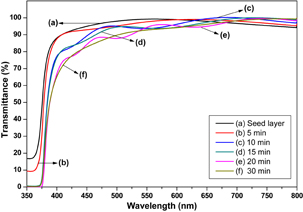
Standard image High-resolution imageThe optical properties of ZnO nanorods are determined using UV–vis–NIR spectrophotometer measurements between 350 and 800 nm at room temperature. Figure 6 illustrates the transmittance spectra of the ZnO nanorod arrays thin film immersed at various growth times. In all cases, the films were transparent, which is defined as above 90% in the visible range. The absorption edges are below 400 nm. This outcome is attributed to the intrinsic ZnO band gap because of the electron transitions from the valence band to the conduction band. The variation in the absorption edges might be caused by the difference in particles size, which has been widely reported in the literature.20–23) Additionally, this shifting may be also attributed to the internal stress produced in the film and the light scattering effects in the films caused by the random distribution of the nanorod arrays.24) The variation in film thicknesses, which slightly depends on growth time, impedes the transmittance when immersion times increase. The highest transmittance was recorded for the seed layer sample with an average transmittance of 96.65% between 400 and 800 nm in the visible region, whereas the lowest transmittance was obtained for the sample immersed at 30 min with an average transmittance of 92.30% on the same wavelength. This result is shown in Table I. Meanwhile, the porosity estimation of the ZnO nanorod array thin films was investigated using the Lorentz–Lorentz equation below:25,26)

where nf is the refractive index of the porous ZnO films and ns is the refractive index of the ZnO skeleton, which is widely accepted as 2.27) Index of refraction nf at different wavelengths was calculated using the envelope curve for transmittance maxima (Tmax) and transmittance minima (Tmin) in the transmission spectra.28) The refractive index is given by the following expressions:

Tm is the envelope function of the Tmax and Tmin, whereas s is the refractive index of the substrate. Tm is obtained by considering the average of the transmittance data from the transparent region or the region where α is close to 0, which is between the 400 and 800 nm wavelength.29) The calculated porosity values for all films are summarized in Table I. The table indicates that the porosity of the ZnO nanorod array thin films tend to decrease with growth time. This outcome may be attributed to the increment in thickness formation of non-uniform micropores and nanopores in the ZnO crystallite structure, which is common for thin films prepared by sol–gel method.29)
Fig. 6. Transmittance spectra of ZnO nanorod arrays prepared at various growth times.
Download figure:
Standard image High-resolution image
4. Conclusions
ZnO nanorod structures were successfully prepared on a glass substrate coated with a ZAO seed layer using a novel dual sonication sol–gel process at various immersion times ranging from 5 to 30 min. The diameter of the prepared ZnO nanorods increased from 65 to 80 nm as the growth time increased. The thickness of the nanorods also increased with immersion time. Besides, the average transmittance of films was above 90% in the wavelength range between 400 and 800 nm. These transmittance values were significantly influenced by the thicknesses of the ZnO nanorod films. These results suggest that varied immersion growth times significantly affect the properties of ZnO films.
Acknowledgments
This work was supported by Grant Nos. 600-RMI/LRGS 5/3 (3/2013), 600-RMI/DANA 5/3/PSI (165/2013), 600-RMI/RACE 16/6/2 (9/2013) and by the Program Ahli Sains dan Penyelidik Muda (PSPM) scholarship under the Ministry of Science and Technology and Innovation (MOSTI), the Ministry of Higher Education (MOHE), and the Universiti Teknologi MARA (UiTM), Malaysia. The authors would like to thank the Research Management Centre (RMC), Universiti Teknologi MARA (UiTM), Malaysia, for their support. This research also was partly supported by the Research Chair for Biomedical Applications of Nanomaterials, Deanship of Scientific Research, King Saud University, Riyadh, Saudi Arabia. The authors also acknowledge the Department of Biochemistry, College of Science, King Saud University, Kingdom of Saudi Arabia for the research collaboration. The authors would also like to thank Professor Datin Ir., Dr. Shah Rizam Mohd Shah Baki, Mr. Salifairus Mohammad Jafar (UiTM Science Officer), Mrs. Nurul Wahida (UiTM Assistant Science Officer), Mr. Mohd Azlan Jaafar (UiTM Assistant Engineer), and Mr. Suhaimi Ahmad (UiTM Assistant Engineer) for their kind support to this research.