
Abstract
We propose a fabrication method for chalcogenide glass (ChG) waveguides based on hot melt smoothing and micro-trench filling. ChGs has low melting points and good flowability. Experiments show that this method can realize high quality As2S7 glass waveguides with reverse ridge structures. The attenuations of the fundamental quasi-TE mode and quasi-TM mode are 0.1 and 0.9 dB/cm, respectively. This method avoids fabrication processes, such as photolithography, lift-off, and dry or wet etching that are directly applied to the ChG films. It provides a simple way to fabricate high quality ChG waveguides, which have great potential for applications in integrated nonlinear optical devices.
Export citation and abstract BibTeX RIS

Content from this work may be used under the terms of the Creative Commons Attribution 4.0 license. Any further distribution of this work must maintain attribution to the author(s) and the title of the work, journal citation and DOI.
Chalcogenide glass waveguides have high third-order nonlinearities,1–3) low two-photon absorption,4,5) and negligible free carrier absorption,6) which are preferred in integrated nonlinear photonic devices.7) However, since the thermal and mechanical properties of ChGs are significantly different from the semiconductor materials widely used in integrated photonic devices, the fabrication techniques of ChG waveguides has become an important topic and attracted much attention.8–11) Usually, the first step in the fabrication of ChG waveguides is the film deposition of ChGs. This can be realized by several methods, such as thermal evaporation,12) sputtering,13) chemical vapor deposition,14) or pulsed laser deposition.15) To reduce scattering loss, the ChG films should undergo an annealing process16–20) to relax the chemical bonds in them.21) Then, waveguide structures may be fabricated on the films in several ways, such as by wet etching,22) dry etching,23) or lift-off.24) In these processes, photolithography or E-beam lithography is required to transfer the waveguide pattern to the ChG film. However, alkaline developers may reduce the quality of the ChG films and waveguides.18) Hence, various techniques of applying protective coating have been developed;25,26) however, they may increase the difficulty of the waveguide fabrication and weaken the transmission properties of the waveguide.25) Recently, the fabrication method of ChG films based on their organic ammonia solution has developed rapidly. However, the residual solvent may lead to obvious loss when it is used to fabricate optical waveguides in the near-infrared band, since its N–H bonds have an overtone absorption around 1510 nm.27)
ChGs have some interesting properties including low glass transition temperatures and low melting points, which may provide new directions for waveguide fabrication. By proper temperature control so as to prevent crystallization, the shape of ChG films may be modified by the melting and flowing processes. In this paper, utilizing this property we propose a simple fabrication method for ChG waveguides based on hot melt smooth and micro-trench filling. The feasibility of the proposed method is demonstrated by waveguide fabrication, sample profile observation, theoretical analysis of the waveguide modes, and measurements of the transmission properties of the waveguide samples.
A sketch of the proposed fabrication process is shown in Fig. 1. Firstly, a micro-trench is fabricated in a silica substrate by photolithography and dry etching or wet etching using buffer fluorhydric acid (BHF), which is shown in Figs. 1(a)–1(c). Then, the ChG film is deposited on the substrate by thermal evaporation or sputtering, which is shown in Fig. 1(d). Finally, the chip is set in a vacuum furnace and annealed at the proper temperature. In this process, the ChG is melted and flows to the trench, leading to a self-smoothing effect. The resulting waveguide is shown in Fig. 1(e), which has a reverse ridge waveguide structure realized by the hot melt smoothing and micro-trench filling processes. To protect the ChG film, an up-cladding layer would be fabricated on it, which could be an SU-8 photoresist or SiO2 layer deposited by sputtering. This method avoids fabrication processes directly applied to the ChG film, such as photolithography, lift-off, or dry or wet etching. Hence, it provides a simple way to fabricate high quality ChG waveguides.

Fig. 1. Fabrication process for ChG waveguides by hot melt smoothing and micro-trench filling.
Download figure:
Standard image High-resolution imageTo demonstrate this simple fabrication process for ChG waveguides, As2S7 glass is used in the experiment since this material has a low melting point and good flowability when it is melted. To help the melting As2S7 glass flow over the micro-trench, the chip is placed with a tilt of 5°. The temperature and duration of the hot melt smoothing process are 210 °C and 3 h, respectively. Figure 2 shows a scanning electron microscopic (SEM) picture of a typical waveguide fabricated by this method. The inset of the figure shows a microscopic picture of the micro-trenches fabricated by wet etching on the silica substrate. It can be seen that by the effect of hot melt smoothing, the As2S7 material fills the micro-trench on the silica substrate, realizing a reverse ridge waveguide. In this sample, the ridge has two sloping sides, which is due to a side etching effect in the wet-etching process.

Fig. 2. SEM picture of the As2S7 waveguide samples fabricated by the proposed method. The inset is a microscopic picture of the micro-trenches fabricated on the silica substrate.
Download figure:
Standard image High-resolution imageTo demonstrate that the As2S7 glass is not oxidized during the hot melt smoothing process, we take an energy-dispersive X-ray spectroscopy (EDX) measurement on a waveguide sample to show the distributions of different elements over the waveguide cross-section. A SEM picture of the waveguide sample is shown in Fig. 3(a), while the distributions of S, O, and As are shown in Figs. 3(b), 3(c), and 3(d), respectively. It can be seen that the material in the ridge region is composed of S and As, while O is distributed in the silica substrate.
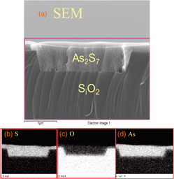
Fig. 3. Measurement results of EDX on a waveguide sample. (a) SEM picture of the waveguide sample. (b)–(d) Distributions of (b) S, (c) O, and (d) As.
Download figure:
Standard image High-resolution imageThe transmission properties of the waveguides fabricated by this method are analyzed theoretically using a finite element method (FEM). The main results are summarized in Fig. 4. Figure 4(a) shows a sketch of the waveguide cross-section. The structure parameters used in the calculation were selected according to the waveguide sample shown in Fig. 2 (H1 = 360 nm, H2 = 700 nm, and W = 5 µm). Since the optical property of As2S7 glass is still unavailable, we use the parameters of As2S3 in the calculation. The refractive index of SiO228) and ChG29) are calculated using the Sellmeier equations. Figures 4(b) and 4(c) show the calculated transverse electric field distributions of the fundamental quasi-TE and quasi-TM modes supported in this waveguide (to simplify the description, the two modes are denoted by quasi-TE and quasi-TM modes, respectively in the following). It can be seen that both modes are well confined by the reverse ridge structure. Figure 4(d) shows the calculated effective indices (indicated by neff) of the two modes. The dispersion curves of the two modes can be calculated using

where D is the dispersion of the transmission mode, and λ and c are the light wavelength and light speed in vacuum, respectively. The calculation results are shown in Fig. 4(e). Since the material dispersion of the ChG is negative near the 1.55 µm band, it can be seen that the impact of the waveguide dispersion of the quasi-TM mode is much stronger than that of quasi-TE mode. In particular, a zero dispersion point is realized around 1.55 µm for the quasi-TM mode, which is preferred in many nonlinear optical applications.

Download figure:
Standard image High-resolution image
Fig. 4. Theoretical analysis on the transmission property of the reverse ridge waveguide. (a) Sketch of the waveguide cross-section. The structure parameters used in the calculation are set as H1 = 360 nm, H2 = 700 nm, and W = 5 µm, which is according to the waveguide sample shown in Fig. 2. (b, c) Electrical field distributions of the fundamental quasi-TE and quasi-TM modes. (d) Calculated neff of the fundamental quasi-TE and quasi-TM modes. (e) Calculated dispersion curves of the fundamental quasi-TE and quasi-TM modes.
Download figure:
Standard image High-resolution imageThen, the transmission properties of the waveguide samples shown in Fig. 5 are measured by an automatic alignment system with a tunable laser (Santec TSL-510). The light is coupled into and out of the waveguide by lensed fibers mounted on the alignment system. A polarization controller (Agilent 11896A) is used to control the light coupling into the quasi-TE or quasi-TM mode of the waveguide. The output light is detected by a power meter (Newport 2936-R).

Fig. 5. Experiment results of the transmission properties of the fabricated waveguides (H1 = 360 nm, H2 = 700 nm, and W = 5 µm). The samples have three waveguide lengths, which are 5, 10, and 18 mm, respectively.
Download figure:
Standard image High-resolution image
We measured the insertion losses of the quasi-TE mode and the quasi-TM mode at 1550 nm in several waveguide samples with different lengths (5, 10, and 18 mm) and show the results in Fig. 5. The attenuation of the quasi-TE mode and the quasi-TM mode in the waveguide samples can be estimated by linear fitting, which are approximately 0.1 and 0.9 dB/cm, respectively, at 1550 nm. On the other hand, the coupling losses between the waveguide and the lensed fibers can be estimated by the intercepts of the fitting line, which are 5.91 and 5.94 dB/facet for the quasi-TE mode and the quasi-TM mode, respectively. The experimental results demonstrate that the proposed fabrication process can realize high quality ChG waveguide fabrication with low loss transmission in the telecom band. The measured attenuation is comparable with that of the best ChG waveguides fabricated by dry etching,23,30) and better than that of the ChG waveguides fabricated by lift-off,24) nano-imprint,8) or the method based on the organic ammonia solution of ChG.27)
In this paper, we proposed a simple fabrication method for ChG waveguides. Utilizing the low melting point and high flowability of ChG materials, reverse ridge waveguides can be fabricated by hot melt smoothing and micro-trench filling. We demonstrate the feasibility of the proposed method using As2S7 glass, which has a low melting point and good flowability. The attenuations of the quasi-TE mode and quasi-TM mode in the typical waveguide samples are 0.1 and 0.9 dB/cm, respectively. While, the coupling losses between lensed fibers and the waveguide samples are ∼5.91 and ∼5.94 dB/facet for the quasi-TE mode and quasi-TM mode, respectively. This method avoids complex fabrication processes directly applied to the ChG film, such as photolithography, lift-off, or dry or wet etching. Hence, it provides a simple way to fabricate high quality ChGs waveguides, which have great potential for applications in integrated nonlinear optical devices.
Acknowledgments
This work was supported by 973 Programs of China under Contract No. 2013CB328704 and 2011CBA00303, the National Natural Science Foundation of China under Contract No. 61575102 and 61321004, and the Basic Research Foundation of Tsinghua National Laboratory for Information Science and Technology (TNList).