

Abstract
We propose a method of realizing a quantum topological transistor in AB-stacked bilayer graphene with Rashba spin–orbit interaction (RSOI) and interlayer bias voltage. It is found that electrons in the proposed device are transmitted in the channels confined at the edges without backscattering, and the resulting perfect conductance plateau can be changed to zero by modulating the interlayer potential difference in bilayer graphene. Our theoretical prediction suggests the possibility of designing a dissipationless quantum transistor in which transport properties are controlled by external gates. The proposed method is useful in the development of electronic devices with low power consumption.
Export citation and abstract BibTeX RIS
Topological insulators are materials characterized by an insulating bulk gap and robust gapless edge states, which have attracted a lot of attention in recent years owing to potential technological applications and new physical properties.1–10) In topological insulators, electrons are transported in channels confined at edges or surfaces without backscattering, and dissipationless quantum transport has attractive practical potentials in the development of electronic devices with low power consumption. Soon after the successful exfoliation of graphene,11) a two-dimensional (2D) topological insulator was predicted in graphene by Kane and Mele,12) which is known as the quantum spin Hall insulator. However, further studies show that the experimental realization of a quantum spin Hall insulator in graphene is not easy owing to an extremely weak intrinsic spin–orbit interaction.13–16) Therefore, the development of various topological phases in 2D materials has attracted extensive research interest.17) A possible approach is to explore other elemental 2D analogues of graphene, such as silicene,18,19) germanene,20) and phosphorene,21,22) and another approach is to exploit multilayer graphenes, among which the simplest is bilayer graphene.
Bilayer graphene is a material consisting of two layers of van der Waals coupled hexagonally arranged carbon atoms, and it has been demonstrated that topological phases can be obtained by applying a perpendicular electric field produced by gate bias.23–26) It has also been shown that the quantum valley Hall effect can be obtained by applying double gates and Rashba spin–orbit interaction (RSOI).27,28) Very recently, topologically protected one-dimensional edge states have been experimentally observed in bilayer graphene,29) which opens up opportunities to explore the topological quantum transport in 2D systems.
Motivated by the very recent experimental realization of topological quantum transport in bilayer graphene30,31) and research interest in the topological edge transport of matter, we study the topological quantum transport in a double-bended bilayer graphene nanoribbon consisting of a combination of armchair and zigzag edges [see Figs. 1(a) and 1(c)]. It is noted in Fig. 1(b) that an interlayer bias can be induced by a perpendicular electric displacement field, which can be realized by adding two gates to the top and bottom layers individually. In the double-bended bilayer graphene region, both RSOI and interlayer bias are included, which induces gate-controllable topological phases. In semi-infinite leads, we only consider an interlayer bias. We investigated the transport properties of our proposed device through the conductance, band structure, and density of states. We found that the conductance of the proposed device is changed from 2e2/h to zero by modulating the interlayer potential difference in bilayer graphene nanoribbons, which means that the device acts as a transistor where the "on" state can be switched to the "off" state by changing the external gate potential. The observation of the local density of states can provide direct evidence of topological edge states, which can be determined experimentally using a spatially resolved scanning tunneling microscope. Moreover, the measurement of the quantized conductance of our proposed device can also provide direct evidence of topological quantum transport. In our numerical calculations, the sample size is chosen to be W = 19.74 nm, L = 9.64 nm, M = 7.50 nm, and D = 24.35 nm.
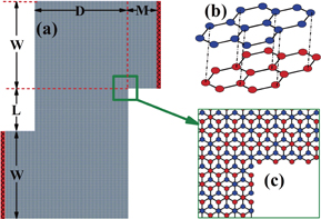
Fig. 1. (a) Schematic illustration of the double-bended bilayer graphene nanoribbon structure. Two semi-infinite leads (red region) are connected to a double-bended structure. (b) Side view of the lattice structure of AB-stacked bilayer graphene. (c) Enlarged view of the part of the figure marked with a square in (a).
Download figure:
Standard image High-resolution imageIn the tight-binding approximation, the Hamiltonian for single-layer graphene in the presence of RSOI can be written as

where  (ciα) is the creation (annihilation) operator of electrons with spin α on site i and
  denotes the summation over nearest neighbor sites. The first term denotes the nearest neighbor hopping in the honeycomb lattice, and the typical hopping amplitude in graphene is t = 2.7 eV.32) The second term denotes RSOI with the coupling strength λR = 0.225 eV,33) which is also described by the nearest hopping in the honeycomb lattice.
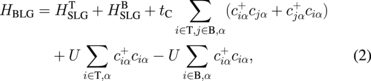
For the AB-stacked bilayer graphene with RSOI and interlayer potential difference, the tight-binding Hamiltonian can be expressed as
where  and
and  are the single-layer Hamiltonians for the top (T) and bottom (B) layers, respectively, which are expressed in Eq. (1). The third term describes the interlayer hopping between the layers with the coupling strength tC = 0.39 eV. The last two terms represent the interlayer bias U applied across the bilayer, and the energy difference between the top and bottom layers is 2U. All numerical calculations were performed using the Kwant tight-binding code.34)
In Fig. 2, we compared the conductances of our proposed device for two different interlayer bias voltages. For U = 0.3 eV (red line), we found that a perfect conductance plateau with the height 2e2/h appears owing to the contribution of the edge channels in the device. When the Fermi energy is larger than 0.11 eV, the conductance shows rapid oscillations with increasing Fermi energy. On the other hand, the conductance is zero for a wide Fermi energy range when the interlayer bias voltage is set at U = 0.7 eV (blue line). Owing to these transport properties, the proposed device can act as a field-effect transistor, where the conductance is quantized and achieved through topologically protected edge states. This quantum topological transistor can be switched between the on and off states with the change in gate voltage. The corresponding local densities of states (LDOSs) for the on and off states are also presented as insets in Fig. 2. It can be noted in the insets that the DOSs are confined at the edges, and that the electrons are only transported in the edge channels. For the off state, we can see that the LDOS only locates at the zigzag edges, and there is no LDOS at the armchair edge. We call this device "quantum transistor" owing to its quantized conductance, which is different from that of a conventional transistor. Moreover, this device has great advantages over conventional transistors because electrons are transported in edge channels without backscattering, which avoids dissipation. Consequently, it was called a topological quantum transistor, which is a promising candidate for next-generation low-power devices.
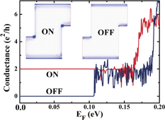
Fig. 2. Conductance of the double-bended bilayer graphene structure plotted as a function of Fermi energy with two different interlayer bias voltages U = 0.3 and 0.7 eV. The insets show the local density of states of the quantum topological transistor for the "on" and "off" states with Ef = 0.01 eV. The other parameters are λR = 0.225 eV, t = 2.7 eV, and tC = 0.39 eV.
Download figure:
Standard image High-resolution imageFor physical understanding of the transport properties shown in Fig. 2, we consider the band structures of bilayer graphene nanoribbons in Fig. 3. As shown in Fig. 2, the conductance has a wide conductance plateau for the on state when the interlayer bias is U = 0.3 eV. Here, we plotted the band structure of each section of the double-bended bilayer graphene structure. The two leads connected to the device are zigzag bilayer graphene nanoribbons, where the Rashba spin orbit interaction is set to be zero and only the interlayer bias is included. We found that a topological phase is obtained for the zigzag bilayer graphene nanoribbon [see Figs. 3(a) and 3(d)], so electrons will transport in gapless edge states while the bulk is insulating. For the double-bended bilayer graphene structure, we have both a zigzag edge (horizontal direction) and an armchair edge (vertical direction). In this region, both the RSOI and the interlayer bias are considered. Similarly, topological phases are obtained for both zigzag and armchair bilayer graphene nanoribbons. We can see that the energy range of the conductance plateau shown in Fig. 2 agrees with the band structures shown in Figs. 3(a)–3(c). The conductance remains at a plateau when the Fermi energy is in the gap, but it oscillates rapidly when both edge and bulk channels contribute to the conductance. For the conductance plateau, electrons are transported in gapless edge states while the bulk is insulating, so dissipationless currents are transported in the transport channels confined at the two edges without backscattering. For the off state, the conductance is zero in a wide energy region, and Figs. 3(d)–3(f) show the band structures of all sections of the double-bended bilayer graphene device. It is noted in Figs. 3(d) and 3(e) that we have gapless edge states in the leads and in the device section with a zigzag bilayer graphene nanoribbon. However, it is interesting to see that we have a band gap without edge states in the armchair bilayer graphene nanoribbon, which produces the off state of our proposed device.
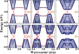
Fig. 3. (a)–(c) Band structure of gated bilayer graphene at a fixed interlayer bias U = 0.3 eV. (d)–(f) Band structure of gated bilayer graphene at a fixed interlayer bias U = 0.7 eV. (a) and (d) are the band structures of the zigzag bilayer graphene nanoribbon with λR = 0. (b) and (e) are the band structures of the zigzag bilayer graphene nanoribbon with λR = 0.225 eV. (c) and (f) are the band structures of the armchair bilayer graphene nanoribbon with λR = 0.225 eV. The other parameters are t = 2.7 eV and tC = 0.39 eV.
Download figure:
Standard image High-resolution imageHere, we take an additional step to explore the dependence of the conductance on the interlayer bias and RSOI for different interlayer coupling strengths. The interlayer coupling sensitively depends on the interlayer separation, which can be modified by external electric fields,35) so we consider two other interlayer coupling strengths, tC = 0.3 and 0.5 eV, in the present study. It is clear in Fig. 4(a) that the proposed device can act as a field-effect transistor, where the on and off states can be obtained by changing the interlayer bias. Note that the conductance remains at a plateau with a height of 2e2/h in a wide region for tC = 0.39 and 0.3 eV. In this region, the conductance is quantized and electrons are transported in the channels confined at the two edges without backscattering. When the interlayer bias is larger than 0.62 eV, the conductance is zero, which means that the system is switched to the off state. However, the conductance is not quantized when the interlayer coupling strength is tC = 0.5 eV, and electrons are transported both at the edges and in the bulk. In Fig. 4(b), we show the dependence of the conductance on RSOI when the interlayer coupling strengths are tC = 0.3, 0.39, and 0.5 eV. We also show that the conductance is zero when RSOI is smaller than 0.15 eV for tC = 0.39 eV, and it increases rapidly with an increase in RSOI. The conductance remains at a plateau with a height of 2e2/h when RSOI is larger than 0.21 eV. Similar numerical results are obtained for tC = 0.3 and 0.5 eV, but the critical RSOI point for reaching the topological transport regime changes with the change in interlayer coupling strength. The critical RSOI point increases with an increase in interlayer coupling strength.

Fig. 4. Conductance plotted as a function of interlayer bias U and RSOI λR for different interlayer coupling strengths. The other parameters are t = 2.7 eV and Ef = 0.02 eV.
Download figure:
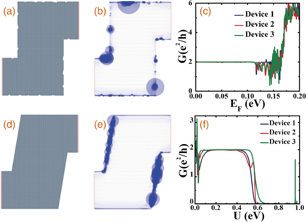
Standard image High-resolution imageIn Fig. 5(a), we present a double-bended bilayer graphene nanoribbon structure that is the same as that shown in Fig. 1(a), but random defects at the edges are considered. It can be seen from Fig. 5(b) that the transport channels are still confined at the edges, although the LDOSs around the defects are enhanced significantly. Electrons can move at the edge of the device while the bulk is insulating. Moreover, we consider the device shown in Fig. 5(d) with the armchair ribbon section lying along a direction (slant edge) different from that in Fig. 5(a) so that the angle between the armchair and zigzag sections is not 90° as in Fig. 5(a). In this case, the edge of the armchair section is not a perfect armchair edge but consists of small sections of armchair edges with a step between two sections. As a result, there are some missing atoms in some hexagon rings along the edge. It is obvious from Fig. 5 that the electrons in this structure can only move at the edges. The LDOSs around the armchair edges are much larger than those around the zigzag edges [see Fig. 5(e)] in the device region, which is different from the perfect armchair nanoribbon (see insets in Fig. 2). To compare the main numerical results of the three different devices, we designate the devices shown in Figs. 1(a), 5(a), and 5(d) as "Device 1", "Device 2", and "Device 3", respectively, and plot in Fig. 5(c) the energy dependence of their conductances. It can be seen that the differences between the three devices are negligible when the Fermi energy is smaller than 0.11 eV. However, the conductances of the three different device structures are markedly different when the Fermi energy is larger than 0.11 eV, owing to the availability of the bulk subbands for electron scattering. The dependence of conductance on the interlayer bias for the three different device structures is shown in Fig. 5(f), and we note that the conductances are the same in the range U = 0.15–0.4 eV. In this energy range, electrons are transported in the channels confined at the edges and the device can be used as a low-power-consumption electronic device. From the results of the above analysis, it can be concluded that the device is immune to defects at the edges and thus can be used as an efficient transistor.
Fig. 5. (a) and (d) Schematic illustrations of Devices 2 and 3. (b) and (e) LDOSs for the devices shown in (a) and (d), respectively, at Fermi energy Ef = 0.01 eV. (c) Conductances of the three devices plotted as a function of Fermi energy with all the parameters being the same as those in Fig. 2. (f) Conductances of the three devices plotted as a function of interlayer bias with the parameters λR = 0.225 eV, t = 2.7 eV, tC = 0.39 eV, and Ef = 0.02 eV.
Download figure:
Standard image High-resolution image
In summary, we propose an effective quantum topological transistor in AB-stacked bilayer graphene in the presence of RSOI and interlayer bias voltage. We investigated theoretically and numerically the transport properties of a double-bended bilayer graphene nanoribbon device through the conductance, LDOS, and band structure. We showed that a gate-controllable quantum topological transistor can be obtained in our proposed structure, where the on state can be switched to the off state through the modulation of the interlayer potential difference. For the on state, we found that a perfect conductance plateau with a height 2e2/h can be obtained, which comes from the edge channels in the device. We also found that the conductance plateau cannot be changed by including random defects at the edges, so the transport properties of the quantum topological transistor are robust. Our theoretical prediction suggests an efficient quantum topological transistor that could have useful applications in the development of topological insulator-based dissipationless devices.
Acknowledgments
This work was supported by the National Natural Science Foundation of China. (NSFC, Grant Nos. 11704078 and 11274260), Guangdong University of Technology One-Hundred Young Talents Program (Project No. 220413143), Science and Technology Program of Guangzhou, China (Grant No. 201707010324), and Key Platforms and Research Projects of the Department of Education of Guangdong Province (2016KTSCX031).