

Abstract
We propose an InGaAs/InAlAs multiple quantum well (MQW) Mach–Zehnder modulator integrated with an array of gap-embedded planar antennas for 60 GHz band radio-over-fiber system. The modulator enables us to directly convert from wireless millimeter-wave (MMW) signals to light-wave signals without any connection cables. A newly designed MQW for the modulator exhibits a large refractive index change at low electric field owing to its unique quantum confined Stark effect, which can achieve push-pull driving in modulation without any external electrical power supply. In addition, by introducing a PIN structure to waveguides, an electric field induced in the antena gap can be applied to a core layer of the waveguide efficiently under the irradiation of MMW signals. The modulator with a 2-element array planar antenna can be driven under an MMW power density of 98 W m−2. We theoretically discuss designs and characteristics of the MQW, planar antenna, and modulator.
Export citation and abstract BibTeX RIS
1. Introduction
Wireless millimeter-wave (MMW) transmission technology has attracted increasing attention for its application to wireless communication services such as fifth-generation mobile communication system, internet of things, and device to device1) instead of a microwave band which is going to be saturated in the near future. In particular, in a 60 GHz band MMW, abundant frequency resources remain in various countries around the world2,3) and it has advantages in high-speed wireless communication as is clear from Shannon's law. In addition, an MMW band has high propagation loss in the air, thus its cell size is small, and frequency utilization efficiency is high. However, a large number of base stations for wireless MMW band communication system are required, and that is why it is necessary to make them network efficient. Radio over fiber (RoF) technology has been used to transfer and relay wireless MMW signals instead of using lossy coaxial cables.4–8)
In the RoF technology, RF signals received by antennas are converted into light-wave (LW) signals by electrooptic (EO) modulators, and then the signals are transmitted with low-loss optical silica fibers. In comparison with using coaxial cables, the transmission using optical fibers not only is a low-loss but also has a large usable bandwidth. Moreover, the transmission scheme is robust against environmental noise, which is advantageous for long haul transmission of wireless MMW signals. As EO modulators between wireless MMW signals and LW signals, lithium-niobate (LN) -based or nonlinear optical polymer-based modulators using EO effects such as Pockels effect or Kerr effect have been used.9–12) In addition, Si- or InP-based modulators using a refractive index change effect such as carrier plasma effect and a light absorption change effect such as quantum confined Stark effect (QCSE)13–16) have also been used. However, coaxial cables are used to transmit the received MMW signals to the modulators, which can result in signal distortion and delay. In particular, in MMW signals, the above issue can appear conspicuously.
On the other hand, EO modulators for directly converting wireless MMW signals into LW signals have been attracted for resolving such problems. For example, phase modulators based on LN17–20) and nonlinear optical polymer,21–23) which are integrated with planar antennas and resonance electrodes, have been reported recently. They enable us to directly convert from wireless MMW signals into LW signals by using an electric field induced in the antennas or the electrodes without using any connection cables and any external power supply. In the researches, a carrier-to-sideband ratio (CSR) of several tens of dB was achieved with an MMW power density P of several hundreds of watts per meter. However, EO coefficients of LN and nonlinear optical polymer are not very large, which causes the modulators to be as large as several centimeters or more. In addition, a Si-based plasmonic phase modulator integrated with plasmonic antenna (plasmotenna) has been reported.24) The plasmotenna makes it possible to induce a huge electric field to the antenna, and miniaturization of the phase modulator can be achieved. In a plasmonic waveguide used in the plasmonic modulator, however, LW signals propagate near a plasmotenna made of metal, which can lead to a significant propagation loss due to metal absorption. In these researches, the phase modulators integrated with antennas have been investigated to convert wireless MMW signals into LW signals. However, intensity modulators integrated with antennas or electrodes have never been reported, although it is in high demand for MMW RoF technology. The reason is that a large device size and high-power consumption are required to realize the intensity modulation, which can make it difficult to obtain a practical one.
To realize the intensity modulator, we propose an InGaAs/InAlAs multiple quantum well (MQW) Mach–Zehnder (MZ) modulator integrated with a multi-element array planar antenna for MMW RoF technology. A preliminary investigation on the modulator such as the design of a planar antenna and the simulation of the MMW characteristics have been reported.25) Because the proposed modulator is based on InP, it can be fabricated monolithically with semiconductor light sources such as a laser diode, which enables us to reduce the footprint of the modulator system. In addition, for the InGaAs/InAlAs MQW, a five-layer asymmetric coupled quantum well (FACQW)26) is newly designed and adopted as a core layer of waveguides in the modulator. Our research group has developed photonic devices using the FACQW such as MZ modulators or switching devices for optical communications.27–30) The proposed FACQW structure is expected to exhibit a giant differential electrorefractive index change ∣Δn/ΔF∣ as large as 4.4 × 10⁻⁴ cm kV−1 in the range of the electric field F of −50 to −60 kV cm−1 owing to its unique QCSE. The electrorefractive index change Δn in the FACQW is expected to be several tens of times larger than that of LN and ten times larger than that of a conventional rectangular quantum well. Therefore, we expect that the proposed InGaAs/InAlAs MQW MZ modulator can achieve miniaturization and low power consumption simultaneously.
In this paper, we design a planar antenna on an InP substrate and analyze the MMW characteristics of the antenna and the proposed modulator at an operational frequency of a 60 GHz band. We also design a new InGaAs/InAlAs FACQW structure that exhibits a large Δn in the electric field region closer to 0 kV cm−1 in comparison with the FACQW reported in Refs. 26–30. The newly designed FACQW enable us to realize modulation operation without any electrical power supply and reduce power consumption. The modulation characteristics of the proposed modulator are also presented. To obtain a high modulation efficiency, the design of the modulator such as an installation position of two arm waveguides are optimized.
2. Electrorefractive index change in InGaAs/InAlAs FACQW
The operational principle of an InGaAs/InAlAs FACQW is summarized in detail in Ref. 26. In this session, the absorption coefficient and electrorefractive index change in the newly designed FACQW are discussed. Figure 1 shows the potential profile of the InGaAs/InAlAs FACQW. It is composed of a 23 monolayer In0.53Ga0.47As QW with a 5 Ml In0.52Al0.48As barrier layer inserted for potential modification and a 17 Ml In0.53Ga0.47As QW. All the layers are lattice-matched to the InP substrate. The positive direction of the applied electric field is defined as illustrated in Fig. 1. In the calculation, the effect of excitons utilizing a nonvariational approach31) and the effect of valence band mixing utilizing the k p perturbation theory with a 4 × 4 Luttinger–Kohn Hamiltonian32,33) are considered.
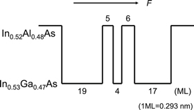
Fig. 1. Potential profile of the InGaAs/InAlAs FACQW.
Download figure:
Standard image High-resolution imageFigure 2 shows the calculated spectra of the absorption coefficient changes in the InGaAs/InAlAs FACQW under the applied electric field of −8 to −16 kV cm−1, which changes are compared with the absorption coefficient under the applied electric field of 0 kV cm−1. With the increase in the electric field, the intensity of the exciton absorption peaks at approximately 1320, 1410 and 1440 nm increases without redshift due to the unique QCSE. The absorption coefficient changes at approximately 1520 nm and in a longer wavelength range are very small. In addition, the InGaAs/InAlAs FACQW is almost transparent in the C-band light of optical fiber communication (1530–1565 nm) because the absorption edge is far from the band.26)

Fig. 2. (Color online) Calculated spectra of the absorption coefficient changes in the InGaAs/InAlAs FACQW under the applied electric field of −8 to −16 kV cm−1. The changes are compared with the absorption coefficient under the applied electric field of 0 kV cm−1.
Download figure:
Standard image High-resolution imageFigure 3 shows the calculated electrorefractive index change Δn in the InGaAs/InAlAs FACQW as a function of the electric field F for the TE mode at the wavelength λ of 1550 nm. The FACQW exhibits a large differential electrorefractive index change ∣Δn/ΔF∣ as large as approximately 4.0 × 10⁻⁴ cm kV−1 at the operation region of the electric field F = −8 to −16 kV cm−1. The DC bias electric field of −12 kV cm−1 is applied to the core layer by using a PIN structure in the waveguide, as described in Sect. 3. Therefore, the modulator can be driven without using any external electrical power supply. In the modulator, the DC bias of −12 kV cm−1 works as the operation point for push-pull driving in modulation.
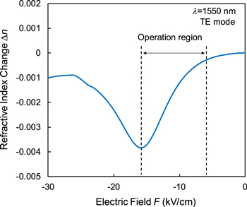
Fig. 3. (Color online) Calculated electrorefractive index change in the InGaAs/InAlAs FACQW as a function of the electric field for TE mode at the wavelength of 1550 nm.
Download figure:
Standard image High-resolution image3. Device structure
Figure 4 shows a schematic view of the InGaAs/InAlAs FACQW MZ modulator integrated with an array of planar antennas. It is composed of an MZ interferometer with two 3 dB multi-mode interference couplers and an array of a multi-element aluminum planar antenna fabricated on the MZ interferometer. By using an array structure, the modulation efficiency can be improved owing to the increase in an accumulated magnitude of the electric field applied to the core layers.20,21) Semi-insulating Fe-doped InP (Fe-InP) is adopted as a substrate to enhance the antenna characteristics. As a structure of planar antennas, we adopted a gap-embedded patch antenna with a micro gap formed in the center of a standard patch antenna.20,21) The gap-embedded patch antenna has a structure similar to a standard patch antenna with a simple structure and a high gain. The gap-embedded patch antenna makes it easy to manufacture and to induce a large electric field in itself. When the patch antenna is irradiated with wireless MMW signals with x-polarization, a displacement current is induced across the gap which results from continuity of a current flow.34) Consequently, a large electric field is induced locally in the gap. In the case of using a standard patch antenna, it is necessary to locate separately two arm waveguides of the MZ interferometer under two sides of the antenna which are perpendicular to an electric field oscillation of the incident MMW signals to apply an electric field to the core layer. Therefore, a propagation loss of the LW signals propagating through the waveguide becomes large due to an increase in its total length. By using the gap-embedded patch antenna, on the other hand, the two waveguides can be located under the narrow gap, as illustrated in Fig. 4, resulting in a reduction in a total length of the waveguide and the propagation loss. Furthermore, by using the electric field of both the positive and negative directions induced in the gap, the modulator can be operated using push-pull driving. The MZ interferometer is buried by benzocyclobutene (BCB) to enhance the electric field applied to its core layer. The BCB also works as an electric field separator between the waveguides. A schematic cross-sectional view of the waveguide is represented in Fig. 5. The core layer is composed of 12-set undoped InGaAs/InAlAs FACQWs and 10 nm InAlAs barrier layers between the FACQWs. The doping densities of the upper p-type InP (p-InP) and lower n-type InP (n-InP) cladding layers were assumed 1.0 × 1017 cm−3. To reduce the absorption loss resulting from the cladding layers and enhance the optical confinement factor, 50 nm undoped InGaAlAs (i-InGaAlAs) layers are inserted as separated-confinement-heterostructure (SCH) layers. The thickness of the multiple FACQW and the total thickness including the SCH layers are approximately 0.3 and 0.4 μm, respectively. All the layers are lattice-matched to the Fe-InP substrate. The electric field applied to the core layer owing to the built-in potential of the PIN structure is calculated to be as large as −12 kV cm−1.
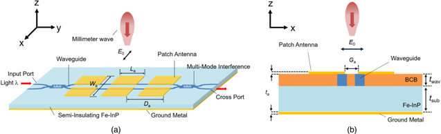
Fig. 4. (Color online) Schematic view of the proposed modulator. (a) Whole view and (b) cross-sectional view in x-z plane.
Download figure:
Standard image High-resolution image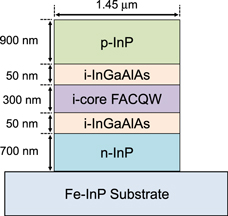
Fig. 5. (Color online) Schematic cross-sectional view of the waveguide structure.
Download figure:
Standard image High-resolution image4. Operation principle
Considering irradiation of a wireless MMW signal at an operational frequency fa, the width of the gap-embedded patch antenna Wa is given by35)

where c is the speed of light in vacuum and εeff is the effective dielectric constant of the patch antenna. The dielectric constant εeff is comparable to the dielectric constant of the Fe-InP substrate (εFe-InP). However, the dielectric constant εeff is affected by installing the gap or a thickness of the Fe-InP substrate. Therefore, a finite element method (FEM) simulator is generally utilized to precisely design an antenna structure with desired antenna characteristics. In this study, we use ANSYS HFSS as the FEM simulator to design the patch antenna and analyze MMW characteristics of the proposed modulator. Figure 6 shows the calculated distribution of the z-component of the electric field Ez on the upper surface of the antenna in the case where a 60 GHz band plane wave with x-polarization is irradiated to the antenna. The magnitude of Ez is normalized with the incident MMW magnitude E0 of 1 V m−1 (Ez/E0). The large electric fields Ez in both positive and negative directions are induced in the gap of the patch antenna, and then the electric fields are applied to the core layer uniformly, as shown in Figs. 6(a) and 6(b). The x- and y-components of the electric field (Ex, Ey) applied to the core layer can be negligible in this study, because the magnitude of Ex and Ey are very small in comparison with that of Ez with any irradiation conditions.
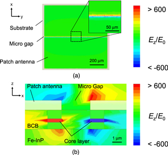
Fig. 6. (Color online) Calculated distribution of the z-component of the electric fields Ez/E0 in (a) the upper surface of the patch antenna and (b) the cross-sectional view of the proposed modulator under irradiation of 60 GHz band MMW plane waves with the incident angle θ of 0°. In the calculation, the antenna length La and the distance between two arm waveguides dwav are set to 900 and 3.0 μm, respectively.
Download figure:
Standard image High-resolution imageFigure 7 shows a schematic view of the modulator under the irradiation of incident MMW plane waves at an incident angle θ. A localized RF wave irradiated by an antenna can be assumed to be a plane wave far from the antenna in far-field regions.35) Considering the irradiation model as illustrated in Fig. 7, an electric field induced across the gap is given by21)

where kRF = 2π/λRF, λRF is the wavelength of the incident RF wave,  is the electric field amplitude, and ωRF is the angular frequency of the RF wave. According to Eq. (2), an increase in θ effectively means that λRF becomes longer. Assuming that the gap-embedded antenna is a combination of many dipole antennas, the electric field induced in the gap is given by21)


where Weff is the effective width of the patch antenna, Ga is the width of the gap, and A(θ) is the scaling factor of the electric field induced in the gap as a function of θ. The width Weff is longer than the actual antenna width due to fringing electric fields generated at the two side edges of the patch antenna along the y-axis. With an increase in Weff, an aperture area of the patch antenna becomes larger, which results in an enhancement of the electric field induced in the gap. The scaling factor A(θ) decreases as increasing in θ, since the effective aperture area of the patch antenna is reduced as described above. In closed-form expressions for the electric field induced in the gap described in Ref. 21, the influence of θ on the electric field was not considered. In this study, A(θ) was introduced to calculate the modulation characteristics of the proposed modulator more precisely. The equivalent refractive index change of the waveguide is given by36)

where neff is the effective refractive index of the core layer, rFACQW is the coefficient of the refractive index change of the FACQW, that is, ∣Δn/ΔF∣, and Γ is the overlap factor between Ez applied to the core layer and an optical field of the LW signal propagating through the core layer. Using the refractive index change given by Eq. (5), the phase difference between the electric field and the optical field over a small distance dy is given by21)

where kop = 2π/λop and λop is the wavelength of the light in vacuum. Assuming that the entrance of the patch antenna is y = 0 and a wavefront entering the gap at time t0 will get to point y in the gap at time  = (neff/c) y + t0, the accumulated phase difference over the patch antenna length of La is given by21)
where u = sinθ −neff. The index u represents the degree of phase mismatching between the electric field and the LW signal, and sin θ = neff means the complete phase matching condition. However, neff is definitely larger than 1 and therefore complete phase matching is not realized. The accumulated phase difference in case of the proposed modulator with an array of N-element gap-embedded patch antennas is given by21)

where Da is the distance between each element of the array patch antenna structure and BN is the scaling factor.
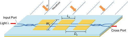
Fig. 7. (Color online) Schematic view of the proposed MZ modulator under irradiation of the incident MMW plane waves with the incident angle of θ.
Download figure:
Standard image High-resolution image5. Antenna design and modulation characteristics
5.1. MMW characteristics
MMW characteristics of the proposed modulator were analyzed by using the FEM simulator. The MMW analysis was performed by irradiating plane wave signals of a 60 GHz band with x-polarization from above the model. The amplitude of the electric field of the incident MMW plane wave is 1 V m−1. The parameters for the MMW analysis were summarized in Table I.
Table I. Parameters for MMW analysis.
| Parameters | Value |
|---|---|
| Waveguide | |
| Distance between two arm waveguides, dwav | 2.4–3.6 μm |
| Thickness, twav | 2 μm |
| Core layer including FACQW | |
| Dielectric constant, εcore | 13.11 |
| Conductivity, σcore | 12 s m−1 |
| p-InP layer | |
| Dielectric constant, εp-InP | 12.35 |
| Conductivity, σp-InP | 480 s m−1 |
| n-InP layer | |
| Dielectric constant, εn-InP | 12.35 |
| Conductivity, σn-InP | 17 200 s m−1 |
| Resin for burying waveguide (BCB) | |
| Dielectric constant, εBCB | 2.7 |
| Thickness, tBCB | 2 μm |
| Substrate (Fe-InP) | |
| Dielectric constant, εFe-InP | 12.49 |
| Conductivity, σFe-InP | 1 × 10⁻⁶ s m−1 |
| Thickness, tsub | 200 μm |
| Gap-embedded patch antenna | |
| Operational frequency, fa | ∼60 GHz |
| Width, Wa | 900 μm |
| Length, La | 600–1200 μm |
| Thickness, ta | 1 μm |
| Gap width, Ga | 3 μm |
| Incident angle, θ | 0°–90° |
Figure 8 shows the calculated magnitude of the z-component of the electric field Ez applied to the core layer and the peak frequency fp as a function of the distance between the two arm waveguides dwav. The electric field Ez is normalized with the magnitude of the incident MMW wave E0 of 1 V m−1. As shown in Fig. 6(b), Ez induced in the gap is radially distributed in the air. Therefore, the installation location of the arm waveguides is important for applying an electric field to the core layer efficiently. The distance dwav was varied with keeping the two waveguides symmetrical against the center of the gap. It is noted that the length of the patch antenna La is 900 μm, and the incident angle θ is 0° in the calculation. The magnitude of Ez was calculated by averaging the electric field applied to an entire core layer (1.45 μm × 0.3 μm × La). The peak frequency fp was defined as the point where the electric field applied to the entire core layer reaches the maximum. When dwav is designed to be as large as 2.8 μm, the magnitude of Ez/E0 reached the maximum. By introducing the PIN structure to the waveguides, the x- and y- components of the electric field induced in the gap can be efficiently applied to the core layer as the z-component of that. With an increase in dwav, fp tends to become higher, as shown in Fig. 8. That is why an increase in the effective dielectric constant εeff of the patch antenna according to Eq. (1), resulting from a decrease in the component of the high-k waveguide (εwav ∼ 12.5). In this study, the distance dwav was designed to be 2.8 μm to apply the large Ez to the core layer while keeping a sufficient space between the arm waveguides to prevent coupling of the LW signals propagating through each arm waveguide.

Fig. 8. (Color online) Calculated magnitude of the z-component of the electric field Ez/E0 and the peak frequency fp of the MMW plane waves as a function of the distance between two arm waveguides dwav. Each broken line is the approximate curve drawn with reference to the plotted data. In the calculation, the patch antenna length La and the incident angle θ are set to 900 μm and 0°, respectively.
Download figure:
Standard image High-resolution imageFigure 9 shows the calculated magnitude of Ez/E0 and the peak frequency fp as a function of the length of the patch antenna La. It is noted that dwav is 3.0 μm and the incident angle θ is 0° in the calculation. The magnitude of Ez/E0 tends to be larger with a decrease in La. In terms of power consumption, however, it is more advantageous on the longer La, since the accumulated magnitude of Ez/E0 becomes larger. The peak frequency also has the same tendency as the magnitude of Ez/E0, which is attributable to the increase in the effective dielectric constant εeff of the patch antenna according to Eq. (1). For modulators integrated with planar antennas, it is necessary to optimize the length of the patch antenna La, that is, a phase shifter length, as seen from Eqs. (7) and (8). In this study, to obtain the large phase difference, La was designed to be 714 μm. The reasons for that are discussed in detail in Sect. 5.2.

Fig. 9. (Color online) Calculated magnitude of the z-component of the electric fields Ez/E0 and the peak frequency fp of the MMW plane waves as a function of the patch antenna length La. Each broken line is the approximate curve drawn with reference to the plotted data. In the calculation, the distance between two arm waveguides dwav and the incident angle θ are set to 3.0 μm and 0°, respectively.
Download figure:
Standard image High-resolution imageFigure 10 shows the calculated magnitude of Ez/E0 as a function of frequency. To achieve the largest applied electric field to the core with the least power, the designed parameters of La and dwav were set to 714 μm and 2.8 μm, respectively. The peak frequency fp of the gap-embedded patch antenna was calculated to be 57.5 GHz. At the peak frequency, the magnitude of Ez/E0 is approximately 800, which means the magnitude of Ez 800 times larger than the incident MMW magnitude E0 can be applied to the core layer. The 3 dB bandwidth of the received power of the patch antenna was approximately 3.5 GHz. Therefore, the modulator with the designed patch antenna can achieve modulation operation in a broad band in the 60 GHz MMW.
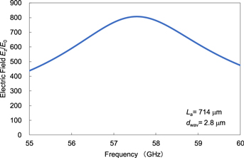
Fig. 10. (Color online) Calculated magnitude of the z-component of the electric fields Ez/E0 as a function of the frequency of the MMW plane waves. In the calculation, the patch antenna length La and the distance between two arm waveguides dwav are set to 714 and 2.8 μm, respectively.
Download figure:
Standard image High-resolution imageFigure 11 shows the calculated magnitude of Ez as a function of the incident angle θ , that is, the scaling factor A(θ), which magnitude is normalized with its largest electric field Ezmax with θ of 0°. In the calculation, La and dwav were set to 900 and 3.0 μm, respectively. The effective aperture area of the patch antenna becomes smaller as an increase in θ as described in Sect. 4, which leads to a decrease in the magnitude of Ez induced in the gap. Accordingly, to maximize the phase change between the arm waveguides with a smaller applied electric field, it is required to optimize the incident angle θ of the MMW signals with considering A(θ), Eqs. (7) and (8).
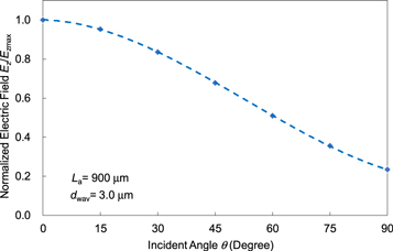
Fig. 11. (Color online) Calculated magnitude of the z-component of the normalized electric field Ez/Ezmax, that is, the scaling factor A(θ), as a function of the incident angle θ of the MMW plane wave. The broken line is the approximate curve drawn with reference to the plotted data. In the calculation, the patch antenna length La and the distance between two arm waveguides dwav are set to 900 and 3.0 μm, respectively.
Download figure:
Standard image High-resolution image5.2. Modulation characteristics
The phase difference and the extinction ratio of the proposed modulator were calculated. In the calculation of the extinction ratio, the modulators with the single patch antenna and N-element array patch antenna are compared. The designed parameters for the modulators were summarized in Table II.
Table II. Designed parameters for proposed modulator.
| Parameters | Value |
|---|---|
| Waveguide | |
| Distance between two arm waveguides, dwav | 2.8 μm |
| Effective refractive index of core layer, neff | 3.84 |
| Operational wavelength | 1.55 μm |
| Array structure | |
| Array number, N | 2 elements |
| Antenna distance, Da | 2514 μm |
| Gap-embedded patch antenna | |
| Operational frequency, fa | ∼58 GHz |
| Length, La | 714 μm |
| Optimal incident angle | ∼19.8° (Single) |
| ∼2.3° (Array) | |
| Total length of proposed modulator | ∼1 mm (Single) |
| ∼3.5 mm (Array) |
Figure 12 shows the calculated phase difference Δϕwav between the arm waveguides as a function of the phase shifter length, that is, the patch antenna length La, which difference is normalized with the largest phase difference Δϕwavmax at the lowest magnitude of Ez to obtain the phase change of π rad. It is noted that the incident angle θ is set to maximize Δϕwav at each phase shifter length La. The normalized phase difference Δϕwav/Δϕwavmax was maximized with La of 714 μm, which indicates that Δϕwav is canceled when the length becomes longer than 714 μm. In the proposed modulator, La is designed to be 714 μm to obtain the phase change of π rad with the least magnitude of Ez, as described in Sect. 5.1.
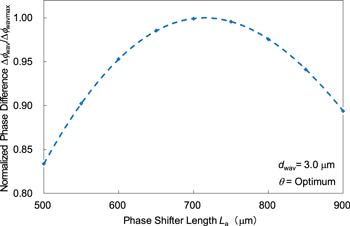
Fig. 12. (Color online) Calculated normalized phase difference Δϕwav/Δϕwavmax between the arm waveguides as a function of the phase shifter length, that is, the patch antenna length La. The broken line is the approximate curve drawn with reference to the plotted data. In the calculation, the distance between two arm waveguides dwav is set to 3.0 μm, and the incident angle θ is set to maximize Δϕwav at each phase shifter length La.
Download figure:
Standard image High-resolution imageFigure 13 shows the static modulation characteristics of the proposed modulator with the single patch antenna under irradiation of the MMW signals. An ideal MZ modulator can achieve infinitely small transmittance when the phase difference between the arm waveguides becomes π rad. In the proposed modulator, the extinction ratios of 10 and 20 dB were obtained when MMW power densities P of 261 and 400 W m−2 were generated around the proposed modulator, respectively. To obtain the phase change of π rad, P of 488 W m−2 is required around the modulator. In the calculation, the incident angle θ was set to 19.8°. As the overlap factor Γ, the calculated optical confinement factor of 0.58 was used.
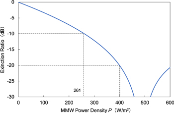
Fig. 13. (Color online) Static modulation characteristics of the proposed modulator with the single patch antenna as a function of the electric power density P generated around the modulator.
Download figure:
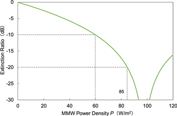
Standard image High-resolution imageFigure 14 shows the static modulation characteristics of the proposed modulator with the 2-element array patch antenna. The extinction ratios of 10 and 20 dB were obtained when MMW power densities P of 60 and 85 W m−2 were generated around the modulator, respectively. In the calculation, with the same condition as Fig. 13, θ and Γ were set to 2.3° and 0.58, respectively. To obtain the phase change of π rad, P of 98 W m−2 is required around the modulator. Assuming that a horn antenna with a gain of 20 dB for irradiation of wireless MMW signals is used from 10 cm above the modulator, the input power for the antenna to obtain the phase change of π rad is approximately 120 mW. The result shows that π phase modulation can be realized with the power consumption which is comparable to that of the phase modulator with antennas or electrodes exhibiting a several tens of CSR,20) while the total length of 3.5 mm is as one-sixth as them.
Fig. 14. (Color online) Static modulation characteristics of the proposed modulator with the 2-element array patch antenna as a function of the electric power density P generated around the modulator.
Download figure:
Standard image High-resolution image
6. Conclusion
We proposed an InGaAs/InAlAs MQW MZ modulator integrated with an array of the gap-embedded planar antennas for directly conversion form wireless MMW signals to LW signals without any connection cables. By using InP as the substrate, the modulator can be fabricated monolithically with semiconductor light sources, which can reduce the footprint of the modulator system significantly. The newly designed InGaAs/InAlAs FACQW as the core layer exhibits a large Δn at the electric field region closer to 0 kV cm−1 due to the unique QCSE. Therefore, the DC bias electric field of −12 kV cm−1 for push-pull driving in modulation can be set just by using the built-in potential of the PIN structure without any external electrical power supply. In addition, by introducing the PIN structure, the electric field induced in the gap can be applied to the core efficiently. For the above reasons, the proposed MQW modulator can achieve compactness and low power consumption simultaneously. We believe that the proposed device is a promising candidate for MMW RoF technology in the future.
Acknowledgments
The authors express sincere thanks to Prof. Joo-Hyong Noh at Kanto Gakuin University for supporting electromagnetic analysis using the FEM simulator. This work was partly supported by a Grant-in-Aid for Scientific Research B (No. 18H01897) from the Ministry of Education, Culture, Sports, Science and Technology.