

Abstract
This work fabricates deep-ultraviolet (DUV) photodetectors (PDs) with a metal-semiconductor-metal structure based on radio-frequency sputtered amorphous Ga2O3 films at room temperature. The Ga2O3-based PD exhibits a low dark current of 1.41 × 10⁻¹¹ A, a responsivity of 1.77 A W−1 and a fast rise response time of 114 ms. A series of annealing treatments with different atmospheres have been found effective to reduce the oxygen vacancy concentration, exhibiting a trade-off effect between the responsivity and the response time. These results demonstrate a cost-effective room-temperature approach for fabricating amorphous Ga2O3-based PDs and developing possible post-synthetic methods for tuning the PD performance.
Export citation and abstract BibTeX RIS
Deep-ultraviolet (DUV) photodetectors (PDs) based on wide-bandgap (WBG) semiconductors have received increasing interest due to a broad range of promising applications. 1–5) Among these materials, Ga2O3 is more suitable for DUV light detection (especially monoclinic phase β-Ga2O3) due to the proper bandgap (4.5–4.9 eV of Eg), good chemical and thermal stability. 6–12) According to previous reports, the DUV light detection performance of β-Ga2O3 films largely depends on the crystal quality, and good crystal quality requires matched growth substrates and high growth temperature, which limits its practical application. 13–16) In recent years, amorphous Ga2O3 has received increasing attention owing to its low growth temperature, non-strict requirements for lattice matching substrate, and large-area preparation capacity. 17–19) In an effort to balance the responsivity and response time of Ga2O3-based PDs, recent experimental and theoretical studies have revealed a profound role of the oxygen vacancy (VO) in Ga2O3 films on tuning the performance of DUV PDs. 20) For example, Guo et al. 21) and Feng et al. 22) reported that VO can significantly improve the conductivity of Ga2O3 films and the response speed of Ga2O3 PDs. Therefore, how to effectively control the VO concentration is the key factor for obtaining PDs with a balanced performance. Annealing is an effective way to regulate the concentration of VO, but current work lacks systematic research on annealing effects in different atmospheres.
In this work, we fabricate DUV PDs with a metal-semiconductor-metal (MSM) structure based on radio-frequency sputtered amorphous Ga2O3 films at room temperature, which exhibits a good responsivity of 1.77 A W−1 and a fast response time of 114 ms. A series of annealing treatments with different atmospheres have been found effective to reduce the VO concentration, which exhibits a trade-off effect on the responsivity and response time. These results demonstrate a cost-effective approach for fabricating amorphous Ga2O3 DUV PDs and explore potential ways for further performance enhancement for practical device application.
Ga2O3 films were deposited on c-sapphire substrates by radio-frequency magnetron sputtering at room temperature. The Ar flow rate, power and work pressure were fixed at 20 sccm, 100 W and 0.5 Pa, respectively. The surface morphology of the as-synthesized Ga2O3 film, labeled as S1, is characterized with atomic force microscopy (AFM), which shows a smooth surface with a roughness of about 1 nm [Fig. 1(a)]. The S1 film consists of densely packed grains, suggesting the characteristic 3D island mode. X-ray diffraction (XRD) scan shows no observable diffraction peak from the S1 film, reflecting the amorphous nature [Fig. 1(b)]. The transmittance spectrum is measured by UV–vis spectroscopy to determine its optical bandgap [Fig. 1(c)]. The S1 film exhibits high transmittance of over 80% in the near-ultraviolet to visible region (300–800 nm), followed by a sharp absorption edge as the excitation wavelength extends through the DUV regime (< 300 nm). The bandgap of S1 is obtained from the (αhν)2 versus hν diagram in the inset in Fig. 1(c), where α is the absorption coefficient and hν the photon energy. 23,24) Fitting the linear region of the curve of (αhν)2 versus hν determines the S1 optical bandgap to be ∼5.09 eV.
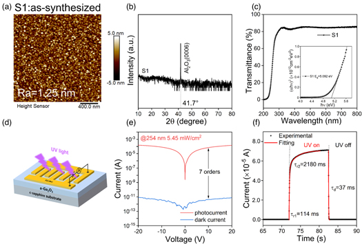
Fig. 1. (Color online) (a) Topography AFM image of the S1 film deposited by radio-frequency magnetron sputtering at room temperature. (b) XRD full scan of the S1 film. (c) The optical transmittance spectra of the S1 film. The inset shows the plot of (αhν)2 versus hν for the S1 film. (d) Schematic of an MSM photodetector. (e) I–V curves of the S1 photodetector in dark and under 254 nm light illumination. (f) I–t curves of the S1 photodetector.
Download figure:
Standard image High-resolution imageTo characterize the photodetection response, interdigital Au (50 nm)/Ti (20 nm) electrodes are deposited on the S1 film [Fig. 1(d)]. The length, width, and spacing of the electrode fingers were 1250 μm, 150 μm, and 150 μm, respectively. The S1 shows a low dark current (Idark) of 1.41 × 10⁻¹¹ A at a bias of 20 V as seen from the current–voltage (I–V) characteristic in Fig. 1(e). Upon illumination with a 254 nm light at 5.45 mW cm−2, the S1 delivers a photocurrent (Iphoto) of 1.45 × 10⁻⁴ A, thus achieving a photo-to-dark current ratio (PDCR) as high as 1.03 × 10⁷ and a responsivity (R) of 1.77 A W−1. Detectivity (D*) as a standard criterion for evaluating the lowest detectable signal. The S1-based PD delivers a high D* of 7.68 × 10¹³ Jones which shows its good ability to detect weak signals. The external quantum efficiency (EQE) represents the ratio of the number of electron-hole pairs collected to the number of incident photons per second, and the S1 has an EQE of 864.67%.
In order to verify the response time of S1, current–time (I–t) characteristics were collected by alternately switching on/off the light source under a fixed bias (20 V). The response time is usually obtained from the fitting resulted based on a double exponential relaxation equation [supplementary data Eq. 1 (available online at stacks.iop.org/APEX/15/022007/mmedia)]. Here the two exponential terms include fast/slow response components, which τr1/τr2 for 10%–90% of the rising process and τd1 /τd2 for 90%–10% of the decay process. Generally, the fast response component corresponds to carrier generation or recombination between intrinsic band edges, and the slow response component corresponds to the carrier trap or detrap process by interband defect states. 15,25,26) The time constants for fast and slow response components of the S1 rising edge are 114 ms (τr1) and 2180 ms (τr2), respectively. The large τr2 value is likely due to the carrier trap process by existing VO defects in S1, 27,28) since no oxygen source is provided during the S1 film growth. Compared to the rising edge, the falling edge of S1 is steeper, and the falling time is 37 ms. Supplementary data Table Ⅰ summarizes the key performance of the PD in this work and other Ga2O3 PDs. Compared with other PDs, the S1 PD exhibits several competitive device characteristics including low current, large PDCR and fast τr1.
Post-annealing has been broadly exploited to modulate the PD performance owing to their strong relation with the film microstructure evolution and defect formation. 20,29) To fully examine the annealing impact, we adopt a medium-temperature (600 ℃) annealing treatment (2 h) to amorphous films in different atmospheres, including neutral atmosphere (air and N2), oxidizing atmosphere (O3) and reducing atmosphere (gas mixture of 95%Ar and 5%H2 volume ratio). The flow of each atmosphere is 100–120 sccm. Among them, the neutral atmosphere is used as a comparative experiment, oxidizing atmosphere and reducing atmosphere are used to explore the regulation of the concentration of VO. The annealed films are labeled as S2 for air, S3 for N2, S4 for O3 and S5 for Ar/H2 (Fig. 2(a)). The morphology of the annealed films showed similar close-packed grains and surface roughness of ∼1 nm to the S1 [Figs. 2(b)–(e)], and the amorphous feature as determined from the XRD patterns [Fig. 2(f)]. All the samples exhibit high transmittance of over 80% in the near-ultraviolet to visible region [Fig. 2(g)]. Their optical bandgaps are close to 5.0 eV with small variation within 0.1 eV [Figs. 2(h) and 2(i)].

Fig. 2. (Color online) (a) Schematic of the post-annealing treatment and corresponding sample information. AFM images of films annealed in (b) S2 air, (c) S3 N2, (d) S4 O3, (e) S5 Ar/H2. (f) XRD full scans of films annealed in different atmospheres. (g) The optical transmittance spectra of the films annealed in different atmospheres. (h) The plot of (αhν)2 versus hν. (i) the bandgap contrast for films annealed in different atmospheres.
Download figure:
Standard image High-resolution imageDespite the negligible influence on surface, structure and optical properties, the annealing treatments have an apparent impact on the carrier transport and photoresponse properties of PDs. As seen from the I–V characteristics in Fig. 3(a), the Idark decreases to a pA range regardless of the annealing atmosphere, suggesting suppression of available free carriers. 28) With the same illumination source, the Iphoto of annealed samples decreases slightly within an order of magnitude [Fig. 3(b)]. More detailed device performance has summarized in Table Ⅰ. Despite the reduced responsivity after annealing, the response time for the fast and slow components simultaneously reduces for all annealed samples [Figs. 3(c) and 3(d)]. The decay edges are very sharp for PDs before and after annealing, which is described by a single time constant (τd). Figure 3(e) summarizes the τr1, τr2 and τd constants of S1-S5 PDs. It is clearly seen that the O3-annealed S4 PD exhibits a maximum reduction of τr1 and τr2 by 55% and 83%, respectively. In addition, the response performance is highly reproducible as seen for the repetition test [Fig. 3(f)].

Fig. 3. (Color online) (a) I–V curves of the S1-S5 photodetectors in dark (b) I–V curves of the S1-S5 photodetectors under 254 nm light illumination (c) Normalized I–t curves of the S1-S5 photodetectors. (d) Magnified diagram of the slow response component at the rising edge of S1-S5 photodetectors. (e) Comparison diagram of the rising edge fast/slow response time component and the falling edge time component of S1-S5 photodetectors. (f) I–t curves of the S1-S5 photodetectors with repetition test.
Download figure:
Standard image High-resolution imageTable I. Key device metric of amorphous Ga2O3 based photodetectors.
| Sample | Idark@20V (A) | Iphoto@20V (A) | PDCR | R (A/W) | D* (Jones) | EQE (%) | τr1/τr2 (ms) | τd (ms) |
|---|---|---|---|---|---|---|---|---|
| S1 | 1.41 × 10⁻¹¹ | 1.45 × 10⁻⁴ | 1.03 × 10⁷ | 1.77 | 7.68 × 10¹³ | 864.67 | 114/2180 | 37 |
| S2 | 1.27 × 10⁻¹² | 1.56 × 10⁻⁵ | 1.23 × 10⁷ | 0.19 | 8.39 × 10¹³ | 93.03 | 48/419 | 36 |
| S3 | 3.37 × 10⁻¹² | 1.19 × 10⁻⁵ | 3.53 × 10⁶ | 0.15 | 4.49 × 10¹³ | 70.96 | 99/666 | 31 |
| S4 | 3.34 × 10⁻¹³ | 6.11 × 10⁻⁶ | 1.83 × 10⁷ | 0.07 | 1.02 × 10¹⁴ | 36.43 | 52/381 | 35 |
| S5 | 1.14 × 10⁻¹² | 6.48 × 10⁻⁶ | 5.68 × 10⁶ | 0.08 | 5.71 × 10¹³ | 38.64 | 56/404 | 38 |
The mechanism of the annealing impact on the device performance is further analyzed from the VO modulation among Ga2O3 films by X-ray photoelectron spectroscopy (XPS). Figures 4(a) and 4(d) show the O1s core level spectra of S1 and S4, respectively. The O1s core level spectra can be fitted with three components by Gaussian fitting. These components are centered at (1) 530.8 ± 0.1 eV (OⅠ), representing O–Ga bonds of Ga2O3; (2) 532.2 ± 0.1 eV (OⅡ), characterizing the O2− ions in the oxygen-deficient regions and generally considered to be VO defects; (3) 533.8 ± 0.1 eV (OⅢ), corresponding to the chemisorbed species on the surface of films. The peak area is used to characterize the relative concentration of each component and the ratio of OⅡ / (OⅠ + OⅡ) can reflect the concentration of VO. 24) The OⅡ peak of the S2–S5 is suppressed, and the calculated OⅡ / (OⅠ + OⅡ) ratio gradually decreases (supplementary data Fig. 1), indicating that the annealing treatment can effectively reduce the VO concentration in the films.

Fig. 4. (Color online) High-resolution XPS spectra of O 1 s core level of (a) S1 and (d) S4. Schematic of the energy band diagram at the interface junction between the metal electrode and the semiconductor for S1 and S4 photodetectors (b), (e) in the dark and (c), (f) under 254 nm light illumination.
Download figure:
Standard image High-resolution image
The energy band diagram of the Ga2O3 PD under dark and illumination conditions are presented in Fig. 4 for discussing the role of VO in the carrier transport process in the PD. From the XPS analysis, S1 has more VO, which could promote electron transport and interface tunneling (Fig. 4b), so the PD exhibits a higher dark current. Upon illumination, the photocarriers trapped by VO at the barrier region are extracted to the external circuit that leads to a higher photoconductive gain and a larger R (Fig. 4c). Such a de-trapping process enabled by a large concentration of VO usually results in persistent photoconductivity (PPC) effect and inevitably makes the response time longer. 28,30) In contrast, the concentration of VO is effectively suppressed after annealing, thereby reducing the capture of photogenerated carriers and increasing the junction barrier height of the devices [Figs. 4(e) and 4(f)], which weakens the internal gain and suppresses the PPC effect. Hence, the annealed devices exhibit lower R while faster response speed. Note that we have regulated the VO concentration in the films by annealing in different atmospheres while the performance of the PDs is not fully optimized, it can be further improved from the aspects of the device structure, crystallinity and annealing temperature in follow-up research. The key function of VO should be carefully handled when optimizing the device performance, since VO could provide free carriers to improve the responsivity, and they can also become deep traps for photocarriers so as to increase the response time. In addition, the following work remains to be explored for amorphous Ga2O3 photodetectors, such as integration of low-cost substrates, carrier modulation with intentional doping and device structure optimization.
In conclusion, we have demonstrated DUV PDs with an MSM structure based on radio-frequency sputtered amorphous Ga2O3 thin films. The Ga2O3 PD exhibits a responsivity of 1.77 A W−1 and a fast rise response time of 114 ms. We further explored a series of annealing treatments to modify the performance of Ga2O3 PDs. It is found that the annealing treatment effectively reduces the response time at the expense of partial responsivity. Such change is related to the VO modulation during the post-annealing treatment. While VO serves as effective donors to provide charge carriers for improving responsivity, they also become trap centers for photogenerated carriers that increase the response time. Our results demonstrate the room-temperature fabrication of high-performance amorphous Ga2O3-based DUV PDs and highlight potential ways for balancing the device performance for DUV light detection.
Acknowledgments
This work was supported by Zhejiang Provincial Natural Science Foundation of China under Grant No. LZ21F040001. N.L. acknowledges the support from China Postdoctoral Science Foundation (No.2021M703313) and the Outstanding Research Associate Funding Project of Chinese Academy of Sciences.