
Abstract
We report on a refractive-index waveguide AlGaN-based ultraviolet-B band (UV-B) laser diode grown on a sapphire substrate, which achieves a laser oscillation at a low threshold current (Ith), ∼85 mA. The refractive index waveguide structure in a ridge-type structure is fabricated by a unique method combining dry inductively coupled plasma reactive ion etching and wet etching with tetramethylammonium hydroxide solution. Using this structure, the longitudinal-mode transverse optical confinement is successfully achieved, in which the ridge width is 3 μm, demonstrating a low Ith of UV-B laser diode.
Export citation and abstract BibTeX RIS
AlGaN-based ultraviolet (UV-) laser diodes have excellent better features of compactness, high efficiency, and low power consumption compared to conventional UV laser sources such as gas lasers (e.g. excimer lasers and He–Cd lasers) and solid-state (e.g. high-order harmonics of YAG lasers) UV laser. Hence, they are expected to be adopted in various applications including microfabrication and biotechnology in the near future. In the last few decades, research and development of AlGaN-based UV laser diodes has been progressed significantly, e.g. pulsed-oscillations of UV-C and UV-B laser diodes have been demonstrated at room temperature (RT). 1,2) Besides, a development of AlGaN-based UV-A laser diodes has been progressed since early 2000s; several research institutes reported the realization of them. 3–7) Based on such basic research, the studies on improving the performance of UV-C and UV-B laser diodes are actively performed nowadays. 8–13)
In the practical point of view, it is very important to demonstrate continuous wave (CW) operation of laser devices at RT. To date, the shortest wavelength of AlGaN-based UV laser diodes under CW operation so far is 348 nm, reported by Cree Inc. 14) Despite the detailed epitaxial structure of the device is still veiled, the device is probably realized on a SiC substrate and is employed an AlGaN active layer. Meanwhile, some information were opened, which includes followings: (i) the laser cavity length and cavity width (p-type electrode width) were ∼500 μm and ∼2 μm, respectively. (ii) The threshold current (Ith) and threshold current density (Jth) of the laser device were ∼58 mA and ∼6 kA cm−2, respectively. As data for further benchmarks, the visible GaInN-based laser diodes under CW operation was achieved Ith, Jth, and operating voltage at laser oscillation (Vth) as low as ∼100 mA, ∼10 kA cm−2, and ∼10 V, respectively. 6,15–24)
As a part of our effort to develop high-performance UV-B laser diodes, we decreased the Jth to ∼13.3 kA cm−2 through improving the carrier injection efficiency, increasing the optical confinement factor, and reducing the internal losses, in gain-waveguided structure. 9) On the other hand, the gain-waveguide structure of the device is considered to have insufficient optical confinement in the lateral direction, i.e. a narrow the p-type electrode increases the optical loss and the Jth. Due to such fact, the p-electrode width increases to 15 μm in the our previous data, which was believed to be wide for nitride-based laser diodes, whereas it results in the high Ith and operating Vth (∼4.0 A and ∼22 V), respectively. Therefore, one possible mean to reduce the Ith and the Vth is believed that the device employs a refractive-index guide structure such as a ridge waveguide structure, which enables to increase the light confinement in the lateral direction. 25–28) That is, when this structure is employed in the device, the Jth is not expected to increase significantly in in spite of the narrowed p-type electrode. Notably, AlGaN-based materials typically do not allow uniform current injection to the active layer due to the high resistance of the p-type cladding layer. For that reason, a novel fabrication method is required to have the same width of ridge with p-type electrode and/or the wider p-type electrode than that of the ridge.
In this study, we examined the refractive-index waveguide structures in ridge structures of laser device to fabricate the high-efficient AlGaN-based UV-B laser diodes. As the unique feature of this study, a method combining inductively coupled plasma reactive ion (ICP) dry etching and wet etching with tetramethylammonium hydroxide (TMAH) solution was utilized to fabricate a ridge structure. It successfully fabricated a slightly inverted tapered shape of the ridge structure, thereby achieving improved refractive index waveguide. We reported and discussed the characteristics of laser diode fabricated by the method proposed in this study.
Figure 1 presents a cross-sectional schematic diagram of the UV-B laser diode with ridge structure. The layer structure of this device is the same as that of the wafer with the lowest Jth among those reported in Ref. 9 using the gain-waveguide structure. The specific layer structure of the device includes a Si-doped (Si concentration of ∼6 × 1018 cm−3) n-Al0.63Ga0.37N cladding layer (∼8.5 μm), a u-Al0.45Ga0.55N first waveguide layer (50 nm), a two-period u-Al0.35Ga0.65N (4 nm)/u-Al0.45Ga0.55N (8 nm) quantum well active layer (2QW), u-Al0.45Ga0.55N second waveguide layer (50 nm), u-Al0.90Ga0.10N electron blocking layer, u-Al0.90→0.60Ga0.10→0.40N (320 nm) first cladding layer, Mg-doped (Mg concentration of ∼3 × 1019 cm−3) p-Al0.60→0Ga0.40→1.00N (75 nm) second cladding layer Mg-doped (Mg concentration of ∼3 × 1019 cm−3) p-GaN contact layer. Note that the Jth in the gain-waveguide structure is a minimum of 13.3–20 kA cm−2 in the layered structure grown under the same conditions and in the device fabricated as a reference, so the results are relatively stable. In this structure, AlGaN was used as the underlying layer, which was grown in three dimensions by spontaneous nucleation to reduce the dislocation density in the subsequent crystals. The interface between the sapphire and AlGaN comprised a layer of high temperature annealed sputtered AlN (SP-AlN), and an AlN homoepitaxial layer (MOVPE-AlN) formed by the metalorganic vapor phase epitaxy method. The dislocation density near the active layer was estimated from cross-sectional scanning transmission electron microscope (STEM) to be approximately 1 × 109 cm−2 in this wafer. The film thickness, Al content, and doping concentration of each layer were adjusted by controlling the growth conditions determined from cross sectional scanning electron microscopy, X-ray diffraction measurements, and secondary ion mass spectrometry measurements.

Fig. 1. (Color online) The cross-sectional schematic diagram of refractive-index waveguide structure in UV-B LD.
Download figure:
Standard image High-resolution imageThe devices were fabricated by laser scribing the wafers into 1 cm square. The process steps for the device were as follows. First, 100 nm thick Ni masks were formed by electron beam deposition using photolithography and lift-off process, and then Cl2 ICP etching was applied to form the ridge stripe shapes. Using the effective refractive index method, the etching depth was set to 370 nm from the p-type GaN surface, a structure that is expected to provide sufficiently high light confinement in the lateral direction in the fundamental mode. This depth corresponds to an etching depth of approximately the vicinity of the guide layer on the p-type layer side. After ICP etching, wet etching was performed using TMAH solution heated to 85 °C using a mantle heater for 5 min. After that, a 250 nm thick SiO2 layer was formed on the ridge by RF sputtering method. Etching Ni with dilute nitric acid in this condition resulted in a structure in which the SiO2 deposited on Ni was almost completely exfoliated to expose p-type GaN. Then, a superior ridge structure was formed with SiO2 coverage on the ridge sides, as explained in the experimental results. On the other hand, without wet etching by TMAH solution, SiO2 deposited on Ni was not peeled off even though Ni was dissolved with dilute nitric acid. In other words, it was suggested that TMAH wet etching had a significant effect on the lift-off of SiO2 on Ni when Ni was stripped.
Then, a mesa structure was formed using a resist mask to expose the n-type Al0.63Ga0.37N layer, and p-type electrodes consisting of Ni/Pt/Au, n-type electrodes consisting of V/Al/Ti/Au, and Ti/Au pad electrodes were deposited on each electrode by electron beam evaporation and formed by a lift-off process. The film thickness and annealing conditions of the electrodes were as described in Ref. 9. The m-plane mirror facets were then formed by using a combined method of Cl2 ICP etching and wet etching with TMAH aqueous solution. 29) After that, the device was characterized in the bar state using laser scribing, leaving both mirror facets of the devices uncoated. In this study, the width of the p-type electrode (ridge width) and the length of the cavity were set to 3 μm and 300 μm, respectively. Afterwards, these devices were characterized under RT and pulsed operation. The integrated light intensity was measured using photomultiplier tube (Hamamatsu photonics, H11901-04MOD) and corrected using a power meter (Ophir, VEGA) through a 1 m length of optical fiber (THORLABS, M114L01) with core diameter of 600 μm which was placed 30 cm far from one side of the mirror facet. The emission spectra from the device edge surface were detected using a spectrometer (Shamrock MCMSM-75 and DU 420A-OE by ANDOR) with a resolution of 0.02 nm. We also investigated the polarization characteristics of the device by using a polarizer. Electrical measurement was performed under pulse conditions (500 ns width, 500 μs cycle constant, 0.001 duty ratio) at RT. In this work, the current density was calculated by dividing the operating current of the laser diode by the p-type electrode area.
Figures 2(a) and 2(b) show cross-sectional STEM images of the fabricated sample and magnified views of its active layer and ridge side area. From both figures, it was confirmed that the side walls of the ridge were stacked with SiO2 and without any gaps. Furthermore, the shape of the ridge was found to be slightly inverted tapered, suggesting that this shape was formed by TMAH wet etching, since ICP dry etching alone resulted in a forward tapered shape. It was also suggested that this shape was a factor in the removal of SiO2 deposited on the Ni mask when the Ni mask was stripped with dilute nitric acid. Furthermore, it was confirmed that the surface of the p-type GaN was completely covered with p-type Ni/Pt/Au electrodes. From the above, it was confirmed that the device has a ridge structure with a superior refractive index waveguide structure.

Fig. 2. (Color online) STEM images of the ridge in the refractive-index waveguide LD. (a) Sectional view. (b) Enlarged view of the side wall of the ridge.
Download figure:
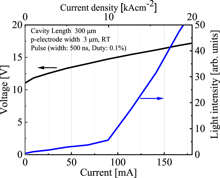
Standard image High-resolution imageFigure 3 presents the I–V and I–L curves of the refractive-index waveguide UV-B laser diode. In this figure, the current density estimated based on the current value and the area of the p-type electrode is shown on the upper axis. The I–L curve showed a clear switch from spontaneous emission to stimulated emission. The threshold current was estimated to be approximately 85 mA, and the threshold current density was found to be roughly 9.4 kA cm−2. The operating voltage of the threshold current for laser oscillation was approximately 14 V.

Fig. 3. (Color online) I–V and I–L curves of UV-B laser diode. The upper axis shows the current density estimated from the current value and electrode area.
Download figure:
Standard image High-resolution imageFigure 4 shows the spectrum at a current value of 149 mA, wherein the polarization characteristics are also confirmed by using a polarizer. The device was confirmed to have longitudinal-mode multimode laser oscillation with TE polarization. The oscillation wavelength was confirmed to be 299 nm. In this laser diode, by forming the good refractive index waveguide structure with the use of a ridge structure, the light confinement in the longitudinal mode lateral direction is good even in a device with a narrow p-type electrode width, and as a result, a deep-UV laser diode with a threshold current of less than 100 mA has been achieved on a sapphire substrate.

Fig. 4. (Color online) Spectra of refractive-index waveguide UV-B laser diode. The polarization properties of the device were investigated by using a polarizer.
Download figure:
Standard image High-resolution image
In summary, we have fabricated refractive-index waveguide AlGaN-based UV-B laser diodes on sapphire substrates. The ridge-waveguide in the UV-B laser diodes was prepared by ICP etching and wet etching with TMAH solution. Room-temperature pulsed oscillation with a lasing wavelength of 299 nm and a threshold current of 85 mA was achieved in the device with the ridge width of 3 μm and the cavity length of 300 μm. Such threshold current is the lowest value among deep UV laser diodes in the literature, and further improvement of the characteristics is expected to realize CW operation in the future.
This study was partially supported by the MEXT Private University Research Branding Project (2016–2020), JSPS KAKENHI (Nos. 16H06415, 16H06416, 15H02019, and 17H01055), JST CREST (JPMJCR16N2), and NEDO Feasibility Study Program.