
Abstract
The performance of perovskite solar cells (PSCs) has been greatly influenced by the surface morphology and orientational growth of organometal halide perovskite, which can be controlled by buffer layers located underneath the perovskite layer. In this study, organic semiconductors such as rubrene and pentacene were selected as the buffer layer materials. We deposited CH3NH3PbI3 (MAPbI3) layers by the laser evaporation method onto the rubrene/pentacene bilayer, pentacene single layer, and rubrene single layer, respectively. The MAPbI3-based solar cell with the rubrene/pentacene bilayer showed a better cell performance compared to other PSCs with rubrene and pentacene single buffer layers. The better PSC performance can be presumably attributed to an orientational growth behavior and a smoother surface of MAPbI3 thin film on the rubrene/pentacene bilayer, as well as a more efficient hole transport in the organic bilayer.
Export citation and abstract BibTeX RIS
1. Introduction
Organic–inorganic hybrid perovskite solar cells (PSCs) have attracted much attention because of their great power conversion efficiency (PCE). Perovskites are one of the desirable materials for the photoactive layer of solar cells in terms of bandgap, light-absorption coefficient, and carrier-diffusion length. 1–3) The PCE reached 25% in 2021. 4) The morphology of the perovskite can affect the charge collection efficiency that is related to PSC performance. 5) In addition, its performance also depends on the orientation of the perovskite as previously reported. 6) It is important to optimize the thin film growth of the perovskite to control the morphology and orientation. We have reported heteroepitaxial growth of CH3NH3PbI3 (MAPbI3) on a rubrene single crystal. 7) However, previous reports used a stand-alone single crystal, which makes it difficult to fabricate PSC devices. A high-crystalline rubrene thin film is required to apply this crystallization method for device fabrication. There had been some technical difficulty in acquiring the high-crystalline rubrene thin film, 8) but Haemori et al. reported the deposition of highly oriented rubrene on a pentacene buffer layer. 9) Therefore, pentacene was used as the base layer material of rubrene in this study. Thus far, organic semiconductor buffer layers (OSBLs) have been incorporated in PSCs to improve their photovoltaic performance. 10,11) OSBLs have various effects on PSCs. For example, they contribute to promoting good contact at the perovskite/electrode interface 12) and realize good alignment of the HOMO level of OSBL to the VB edge of perovskite. 13) In addition, Ryu et al. reported that a deep HOMO level of the hole transport layer improves the VOC of PSC. 14) Rubrene and pentacene can be used as hole transport layers of PSCs because of their high hole mobility (rubrene: 18 cm2 V−1 s−1, pentacene: 1 cm2 V−1 s−1). 15,16) Yang et al. reported the PSC using pentacene as a buffer layer material. 17) In their research, perovskite was deposited on a pentacene buffer layer by spin-coating, where the solvent (N,N-dimethylformamide, dimethyl sulfoxide) could give some damage to the pentacene underlayer, so we adopted a dry process as an alternative way to deposit MAPbI3 on OSBL surfaces. In this paper, we used a rubrene/pentacene bilayer, pentacene layer, and rubrene layer as OSBLs in PSCs to compare the influences of crystallinity and morphology of perovskites grown on these OSBLs on the device performance. The fabrication of PSCs using rubrene as a buffer layer material was added to this paper newly from the SSDM2023 Extended Abstract. 18)
2. Experimental methods
An ITO-coated glass substrate was treated in RF-generated oxygen plasma (3.5 × 10² Pa, 30 min). Poly(3,4-ethylenedioxythiophene):poly(styrenesulfonate) (PEDOT:PSS, Clevious, AI4083), which acts as a conductive organic polymer, 19) was spin-coated on the substrate at 500 rpm for 5 s and 3000 rpm for 180 s. Then, the film was annealed at 135 °C for 10 min. The sample was transferred into the laser evaporation chamber for organic materials where an 808 nm continuous-wave (CW) semiconductor laser was used to evaporate the materials. A pentacene layer (35 nm) was deposited on the PEDOT:PSS by laser evaporation while controlling the substrate temperature at 55 °C. A rubrene layer (15 nm) was deposited on pentacene by laser evaporation with the same substrate temperature (55 °C). Then the sample was transferred into a different laser evaporation chamber (808 nm CW laser) that enables alternative evaporation of PbI2 and CH3NH3I (MAI) (Fig. 1). A PbI2 layer was initially deposited followed by a MAI layer and this process was repeated to form MAPbI3 thin films. Silicon powder was mixed into the MAI and PbI2 target to absorb the laser energy and promote heating of the source materials. 20) The laser for MAI was modulated as a 10 Hz square wave to control the deposition rate of MAI accurately by tuning the duty ratio of the square wave. 20) The sample was transferred into the laser evaporation chamber for organic materials again and a C60 layer (7 nm) was deposited on the MAPbI3 without heating the substrate. C60 is one of the great electron transport materials because of its high electron mobility (1.6 cm2 V−1 s−1). 21) A bathocuproine (BCP) layer (3 nm) was deposited on the C60 by laser evaporation without heating the substrate. Ag electrodes (100 nm) were deposited on the BCP by thermal evaporation without heating the substrate. BCP can suppress the quenching of exciton at the C60/Ag interface. 22) The structures of PSCs prepared in this study are shown in Fig. 2. Crystallinity of the samples was analyzed by X-ray diffraction (XRD, RIGAKU Smart Lab, Cu Kα1 X-ray source). The surface morphologies of the thin films were observed by atomic force microscopy (AFM; Nanonavi/E-sweep, SII nanotechnology).
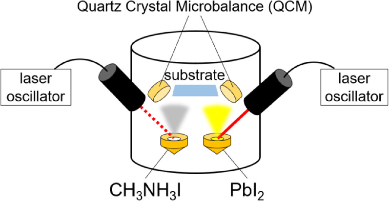
Fig. 1. Schematic diagram of the layer-by-layer laser evaporation chamber.
Download figure:
Standard image High-resolution image
Fig. 2. (a) The molecular structure of rubrene, schematic cross section of PSCs with (b) rubrene/pentacene, (c) pentacene, and (d) rubrene.
Download figure:
Standard image High-resolution image3. Results and discussion
Figure 3 shows the out-of-plane XRD pattern of pentacene film deposited on amorphous PEDOT:PSS to confirm the orientation of pentacene film. The (001) diffraction peak of pentacene (thin film phase) 23) was observed. Out-of-plane XRD patterns of rubrene films deposited on pentacene and PEDOT:PSS are shown in Fig. 4 to demonstrate the importance of the pentacene underlayer. The (002) diffraction peak of rubrene (orthorhombic phase 24)) was observed only for the film deposited on pentacene. The result of the previous research 9) was confirmed, where the out-of-plane orientation of rubrene can be obtained by growing on pentacene. AFM images of rubrene films deposited on pentacene and PEDOT:PSS are shown in Figs. S1(a) and S1(b), respectively, where clear step and terrace structures are seen in the rubrene thin film deposited on pentacene. These results are consistent with Fig. 4. Figure 5 shows AFM images of MAPbI3 thin films (∼30 nm) to investigate the effects of OSBL on MAPbI3 film structure. MAPbI3 fabricated on rubrene/pentacene [Fig. 5(a)] and pentacene [Fig. 5(b)] have a smoother surface than that grown on rubrene [Fig. 5(c)], where root mean square values are 1.23 nm, 0.94 nm, and 2.03 nm, respectively. We attributed these results to the difference in crystallinity. As seen in Figs. 3 and 4, the rubrene/pentacene bilayer and pentacene layer have out-of-plane orientation, while the rubrene layer is amorphous. Thus, highly oriented OSBLs are enhanced to grow smooth MAPbI3 film. Figure S1(d) shows the AFM image of perovskite film on PEDOT:PSS. The perovskite film deposited on PEDOT:PSS contains particle-shaped morphology with a size of 100 nm. The perovskite film deposited on the rubrene/pentacene bilayer shows smoother morphology because of the highly crystalline characteristics of the underlayer. For comparing OSBLs in terms of device performance, J–V curves of PSCs and their performance parameters are shown in Fig. 6 and Table I, respectively. The device using a rubrene/pentacene bilayer as an OSBL exhibited the highest PCE (8.50%) among (a)–(c). The energy level diagrams of PSCs are shown in Fig. 7 following previous reports 1,17,25,26) to discuss the effect of energy level on VOC. The HOMO level of the HTL adjacent to the MAPbI3 layer is deeper in the PSC with rubrene/pentacene than that with only pentacene. This difference can lead to the improvement of VOC (0.61 V→0.89 V) comparing Figs. 6(a) and 6(b). The high crystallinity and reduced voids comparing Figs. 6(a) and 6(c) result in the improvement of JSC (12.40 mA cm−2→16.64 mA cm−2). The voids can decline JSC by decreasing the area that the photocurrent passes. The slight difference in JSC between Figs. 6(a) and 6(b) appears for the same reason observed in Figs. 5(a) and S1(b). The EQE spectra shown in Fig. S3 also suggest that the PSC with only rubrene OSBL has the least JSC in three types of devices. Furthermore, in Fig. 6(c), non-linear resistance appears near VOC. It suggests that carrier transport at the interface between the perovskite and HTL is inhibited. Figure 8 shows the out-of-plane (a) and in-plane (b) XRD patterns of MAPbI3 thin film (∼30 nm) deposited on the rubrene/pentacene bilayer to confirm the orientation of MAPbI3 film. These patterns suggest that the MAPbI3 film is a tetragonal structure. 27,28) Only (002) diffraction peaks of MAPbI3 were detected in Fig. 8(a). This result supports that the MAPbI3 film is highly controlled to form an out-of-plane orientation. In Fig. 8(b), the peak marked with an asterisk was assigned to the (310) diffraction peak of MAPbI3 according to previous research. 29,30) Because the in-plane orientation of the rubrene thin film in this research is not controlled, that of the MAPbI3 film is random. Incidentally, Fig. 9 shows the predicted structural model of MAPbI3 film on rubrene and 〈110〉 and 〈002〉 plane directions are depicted by black arrows.

Fig. 3. Out-of-plane XRD pattern of pentacene film deposited on PEDOT:PSS.
Download figure:
Standard image High-resolution image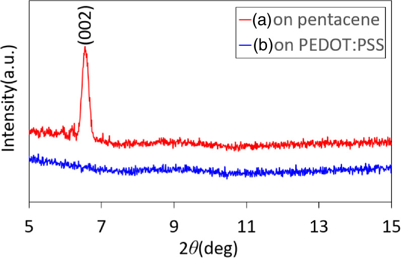
Fig. 4. Out-of-plane XRD patterns of rubrene films deposited on (a) pentacene and (b) PEDOT:PSS.
Download figure:
Standard image High-resolution image
Fig. 5. 2 μm × 2 μm AFM images of MAPbI3 thin films deposited on (a) rubrene/pentacene, (b) pentacene, and (c) rubrene.
Download figure:
Standard image High-resolution image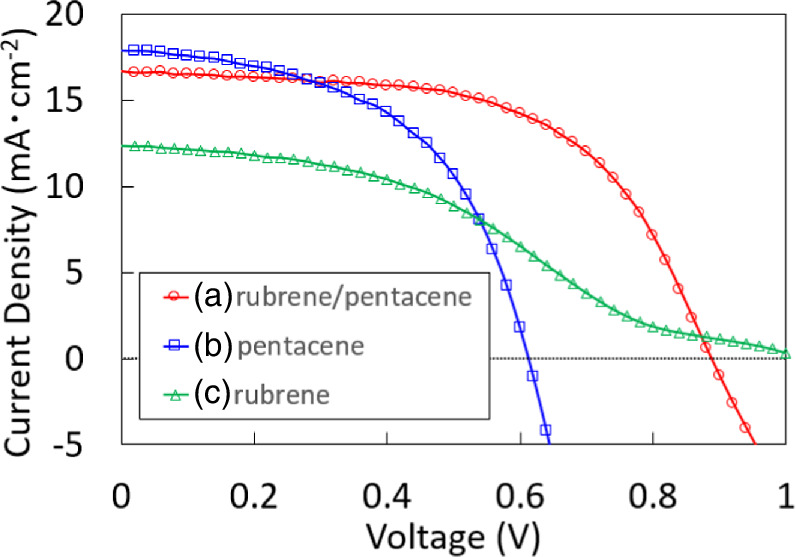
Fig. 6. J–V curves of PSCs with (a) rubrene/pentacene, (b) pentacene, and (c) rubrene.
Download figure:
Standard image High-resolution imageTable I. Summary of device performance parameters of the PSCs with (a) rubrene/pentacene, (b) pentacene, and (c) rubrene.
| OSBL | Voc (V) | Jsc (mA·cm−2) | FF | PCE (%) |
|---|---|---|---|---|
| (a) Rubrene/pentacene | 0.89 | 16.64 | 0.58 | 8.50 |
| (b) Pentacene | 0.61 | 17.88 | 0.52 | 5.68 |
| (c) Rubrene | 1.02 | 12.40 | 0.35 | 4.49 |

Fig. 7. Energy level diagrams of PSCs (a) with and (b) without rubrene (units: eV).
Download figure:
Standard image High-resolution image
Fig. 8. XRD patterns of MAPbI3 thin film deposited on rubrene/pentacene bilayer. (a) Out-of-plane and (b) in-plane.
Download figure:
Standard image High-resolution image
Fig. 9. Structural model of MAPbI3 film on rubrene (side view).
Download figure:
Standard image High-resolution image
4. Conclusions
In this study, we used three types of OSBLs as underlayers of MAPbI3 films, (a) rubrene/pentacene bilayer, (b) pentacene layer, and (c) rubrene layer and investigated the crystal orientation of each layer to compare their PSC performance. A MAPbI3 thin film grown on (a) achieved pronounced out-of-plane orientation and smooth surface morphology. The difference in HOMO level between rubrene and pentacene led to higher VOC of the PSC using (a) than (b). The PSC using (c) showed a lower JSC than (a). because there are a lot of voids in the MAPbI3 film grown on (c). Therefore, among (a)–(c), the greatest OSBL is (a), the rubrene/pentacene bilayer, which achieves improvement in crystallinity and highly efficient charge transport. The importance of a buffer layer in the PSC was verified in terms of both energy level alignment and crystallinity control of the perovskite film. We hope that this research will help to choose the new buffer layer material of the PSC that contributes to improving the crystallinity of the perovskite.
Acknowledgments
This work was supported by JST SPRING, Grant No. MJSP2123 and JSPS KAKENHI, Grant Nos. 20H02819, 20H02838, and 22H01946.
Supplementary data (0.5 MB DOCX)