
Abstract
Here, we proposed two delay lines consisting of spoof surface plasmon polariton (sSPP) waveguides and C-shaped metamaterials (C-MMs). The delay lines, namely OFF and ON devices, were designed and fabricated. On the OFF device, an sSPP waveguide is capacitively coupled to the C-MMs via an air gap on a high-resistivity silicon substrate. On the ON device, a connection is established between the C-MMs and the sSPP waveguide by metal connectors. The difference in the electrical properties in the coupling between the C-MMs and the sSPP waveguide creates a large phase contrast between the ON and OFF delay lines. The structural design was performed using a numerical calculation based on a commercial finite element solver. We successfully fabricated and characterized delay lines with phase differences equal to tens of degrees between the ON and OFF devices in the target frequency range of 2–6 GHz, while maintaining the original transmittance properties. The promising applications of the delay lines are a phase shifter or modulator when integrating with suitable switches.
Export citation and abstract BibTeX RIS
1. Introduction
With the proliferation of fifth-generation mobile communication systems (5G), microwave technology is becoming increasingly important. Microwave signal manipulation is primarily performed in metal waveguide circuits. In particular, phase control is an essential technology for antenna directivity control, delay circuits, and signal processing. In the 5G communication band, controlling the phase using semiconductor elements remains possible. However, as the frequency of mobile communication systems increases toward the next generation, so-called sixth-generation mobile communication systems (6G), the frequency response of semiconductor materials will reach its limit, and new signal control technologies are expected to be developed. It is expected that 5G and 6G communication systems will coexist in the future. Therefore, the realization of a phase shifter or phase modulation device that operates on a common principle from the several GHz frequencies used in 5G communications to the hundreds of GHz frequencies used in 6G communications is expected to become a fundamental element of future 5G/6G communication technology.
In the circuit design, a delay line produces delay effects by gradually slowing down a signal with minimum attenuation. Designing two delay lines with the same transmission characteristics and a phase difference is the first step to developing a phase shifter or modulator when integrating with appropriate switches. As a transmission line is utilized to implement delay lines, the time for a signal to propagate through the device is given by:  where f and k are the frequency and propagation constant, respectively; L is the length of the transmission line. Both the length of the transmission line and the phase constant can be used to adjust the amount of time delay for signals to propagate through the device or the phase tuning. For manipulation of group delay, conventional technology changes the length (L) of the transmission line which leads to a large insertion loss, while the variation of the propagation constant remains challenging.
Spoof surface plasmon polaritons (sSPP) are surface electromagnetic waves in the microwave and terahertz regimes that propagate via a planar interface between stubs and a dielectric medium as transverse modes of surface plasmons. 1) sSPP are widely used in microwave devices due to their high field confinement at subwavelength scales and low transmission loss, which allow the miniaturization of on-chip integrated devices. sSPP waveguide's working mechanism is based on the excitation of surface plasmon polaritons, which have many applications in the microwave range, such as power dividers, 2) frequency splitters, 3) antennas, 4) filters, 5) and potentially various applications in the terahertz range. 6–9) sSPP waveguide has been used for designing delay lines based on propagation constant variation. Mehmet Unlu et al. demonstrated delay lines based on sSPP waveguide which have various phase differences by designing different corrugation depths for the microwave and terahertz range. 10,11) However, these delay lines do not allow tuning the corrugation depths on one device by using switches for the realization of a phase shifter or modulator in the microwave range.
Metamaterials are composed of unit structures that are smaller than the wavelength of the electromagnetic waves to be controlled. These structures have attracted much attention in recent years because resulting artificial optical materials can realize electromagnetic wave responses that do not exist in nature. The unit structure operates as the smallest optical resonator in which the spatially localized electric field mode (optical density of states) can be designed to suit certain needs. Furthermore, the response characteristics of electromagnetic waves are mainly determined by the shape of the metamaterial. Since the discovery of J. Pendry, 12) there has been rapid development of metamaterials which have been applied widely as perfect absorbers, filters, etc., in the visible light, IR, and terahertz frequency ranges. 6,7,13–25) However, to the best knowledge of the authors, there has been no publication on the integration of metamaterial into an sSPP waveguide for the demonstration of delay lines.
The conventional technology for sSPP waveguide manufacturing is based on the RF printed circuit board (PCB). 26–28) However, there are several issues associated with this technique, such as challenges associated with integrating microstructures that are smaller than typical fabrication errors. Because of its improved precision, micromachining technology on silicon substrates, which has been well established, can enable the fabrication of on-chip integrated sSPP devices based on silicon technology.
Here, we propose two delay lines consisting of sSPP waveguides integrating with a novel C-shaped metamaterial (abbreviated as C-MMs) on a silicon substrate in the frequency range of 2–6 GHz. The two delay lines, namely ON and OFF devices, are designed and fabricated. A phase difference for the ON and OFF devices is achieved by the structural difference between the two delay lines with and without electrical connection between the C-MMs and the sSPP waveguide by metal microstructures. Although this phase difference significantly differs between ON and OFF devices, the overall transmittance changes minimally in the frequency range of 2–6 GHz, resulting in useful device characteristics promising for the realization of phase shifters or modulators in one device when suitable switches are integrated.
2. Design and simulation
Two delay lines, namely ON and OFF devices, were designed. These devices mainly consist of an sSPP waveguide and C-shaped metamaterials (C-MMs) groups. Both devices are constituted of five sections: a delay Sect. 1; two triangular transition Sect. 2 and two co-planar waveguide (CPW) sections as shown in Fig. 1(a). In the delay section, four periodic corrugated rectangular metallic structures, the so-called stubs, are coupled with eight metallic C-MMs groups on both sides; two nearby stubs are connected by a central line as indicated in Figs. 1(b), 1(c). Each C-MMs has a square shape with the same dimensions as the width of the stubs (wg) and consists of a total of 16 C-shaped structures with two groups symmetrically facing each other by a gap of g2 . Each of these structures has a width of w3 equal to 50 μm, and the gaps between them for w2 are 50 μm, as shown in the insets in Fig. 1(b). The difference between the two devices is in the main units of the delay section, where the coupling between the C-MMs and the stubs is realized capacitively by an air gap for the OFF device [Fig. 1(b)]; and electrically by metallic connectors which has a width of w1 , for the ON device [Fig. 1(c)].
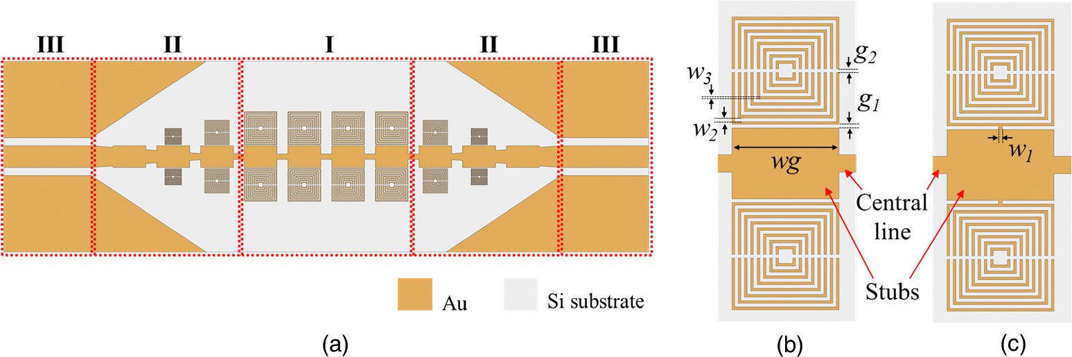
Fig. 1. (a) Geometric model of the proposed delay lines: delay Sect. 1, triangular transition Sect. 2, and CPW Sect. 3. One main unit of the delay section of (b) the OFF device and (c) the ON device.
Download figure:
Standard image High-resolution imageThe sSPP waveguide is designed based on a well-known transmission line called a planar Goubau line which has a single, extremely thin wire positioned on top of a supporting dielectric substrate. 29) The delay section is designed as a Goubau line which consists of four main units, and it can be connected to a 50 Ohm impedance connector by using a CPW which is defined as the Sect. 3 in Fig. 1(a). There are several types of waveguides for the microwave frequency range: co-planar, microstrip, grounded co-planar, and so on. CPW structure allows an electromagnetic field distributed almost on the surface of the substrate. In our devices, it is the silicon substrate that has a high relative permittivity coefficient (ε = 11.7) leading to high dielectric loss. By using a CPW structure, the electromagnetic field does not distribute in the bulk of the silicon substrate which lowers the dielectric loss.
As a result, a transition from the delay sections to the CPW sections is required. The role of the transition units is for mode conversion and momentum matching. 22,30) By using a gradient-index meta-surface, the spatial propagating waves from external sources, such as microwaves from coaxial cables, could be converted into SPPs efficiently. 31) Based on the transition design in Ref. 30, triangular transition sections are used for our devices. In the transition Sect. 2 shown in Fig. 1(a), C-MMs's dimension is scaled down with a ratio of 0.5 and 0.75 relative to that in the main unit, and the width of the central line gradually decreases.
The RF module in COMSOL Multiphysics 6.1 (COMSOL, Inc.) is used for finite element modeling to optimize the devices' performance. In the finite element model, the device is surrounded by an air block with exterior interfaces modeled as scattering boundary conditions to avoid the reflection of electromagnetic waves back into the device, as shown in Fig. 2(a). The metal pattern structure formed on the Si substrate was subjected to transition boundary conditions to account for the skin depth effects caused by the metal thickness of 1100 nm, as in the fabricated devices.
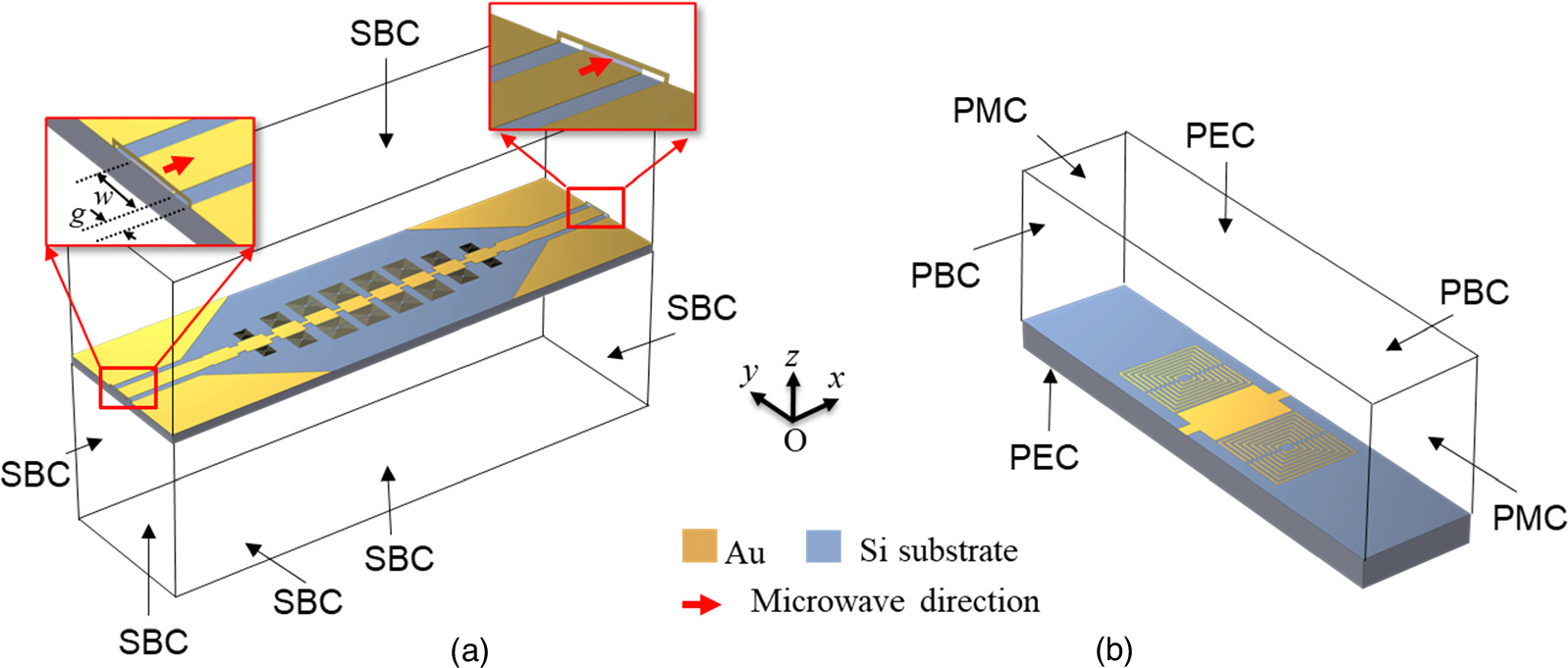
Fig. 2. Boundary conditions for the exterior faces of the (a) sSPP waveguide integrated with C-MMs (the insets are the lumped ports for microwave excitation and output) and (b) one main unit of the OFF device for numerical calculation of the dispersion relation.
Download figure:
Standard image High-resolution imageThe microwave is excited at the left Lumped Port and outputs at the right one as shown in the insets of Fig. 2(a). The dimensions of the two ports, the input port, and the output port are designed based on the CPW geometry, which is calculated to be compatible with an impedance of 50 Ohm for a substrate with a 1 mm thickness and a relative permittivity of 11.7. The width of the transmission line (w); and the gap between the transmission line and the ground metal (g) shown in the insets of Fig. 2(a) are calculated to be 2 mm and 0.73 mm, respectively, which are compatible with the dimensions of subminiature type A (SMA) connectors. The loss tangent of the substrate is set as 0.0001.
Eigenfrequency analysis was implemented to numerically calculate the dispersion relation of the sSPP waveguides. The simulation was applied to one main unit of the delay section in the ON or OFF device. Because the eigenfrequency analysis is different from the efficiency analysis, the Wave Optics Module was used instead of the RF Module of COMSOL Multiphysics in this calculation. Notably, the solution would not converge if the transition boundary condition used for the metal structures at the RF module was used for the eigenfrequency analysis; therefore, perfect electric conductors (PEC) were used to characterize the metal structure in the study of the eigenfrequency analysis. For the exterior faces of the main unit cell, periodic boundary conditions are applied to two faces parallel to the Oyz-plane with the Floquet periodicity type; PEC is applied to two faces parallel to the Oxy-plane, and perfect magnetic conductors are applied to the two faces parallel to the Oxz-plane, as shown in Fig. 2(b).
First, parametric sweeping simulations were carried out on the devices with the sSPP waveguide only, i.e. without C-MMs groups, to determine the transmission characteristics (the S21 parameter) under the influence of dimension parameters such as the height of the grooves (hg), width of the stubs (wg) and pitch (p) between the main units of the sSPP waveguide. These dimension parameters (hg, wg, p) are shown in Fig. 3(a), which describes two main units of the sSPP waveguide. The corresponding dimension values are shown in Table I.

Fig. 3. (a) Structural dimensions of the sSPP waveguide. (b)–(d) The influence of the wg, hg, and p structural parameters on the magnitude of |S21 | in dB; the insets plot the dependence of the cutoff frequency (fc ) on wg, hg, and p. (e) The distribution of the electric field in the y-direction ( E y ) on the waveguide at the cutoff frequency (the color legend is displayed on the linear symmetric scale).
Download figure:
Standard image High-resolution imageTable I. Dimension parameters of the SSPP waveguide in the parametric study.
| wg | hg | p | |
|---|---|---|---|
| wg sweeping | 2–5 mm | 0.95 mm | 4 mm |
| hg sweeping | 3 mm | 0.55–0.99 mm | 4 mm |
| p sweeping | 3 mm | 0.95 mm | 3.1–5 mm |
From the simulated results in Figs. 3(b)–3(d), the transmission band of the sSPP waveguide shows operation as a low-pass filter with a cutoff frequency (fc ). The cutoff frequency is defined as the frequency at which the signal's pass gain is 3 dB lower than the passband (the amplitude is attenuated by 30%). As illustrated in Fig. 3(e), the electromagnetic field propagation discontinues in the middle of the transmission line at the cutoff frequency. The dependence of the cutoff frequency on structural parameters (wg, hg, and p) is displayed in the insets of Figs. 3(b)–3(d), respectively. From the numerical calculation, as the parameters wg, hg, and p increase, the cutoff frequency of the sSPP waveguide decreases. The transmission in the frequency range of interest for 2–6 GHz is almost unchanged in all the parametric simulations.
When the C-MMs are integrated into the sSPP waveguide as the OFF device [Fig. 4(a)], a notch band occurs at a frequency (fn ) of 8.9 GHz, corresponding to a transmission characteristic as the air gap g1 is 1000 μm; this band is generated due to the reflection of microwaves at the resonant frequency of the C-MMs, as the yellow curve in Fig. 4(b). At high frequencies smaller than the fn , the microwave is propagating through the device with high transmittance. As a result, the electric field is confined within the gaps of the C-MMs as well as between the C-MMs and stubs, while the magnetic field is confined to the grooves of the transmission line, as shown in Figs. 4(b) and 4(c). It has thus been proven that C-MMs are a type of metamaterial that can strongly confine electromagnetic field and the field confinement allows transmission of microwave and terahertz waves which have much longer wavelength than the sSPP waveguide's dimensions. Therefore, the sSPP waveguide is an ideal candidate to provide new, compact integrated systems, accelerating applications in high-resolution imaging, spectroscopy, and next-generation ultra-wideband communications. 32) Furthermore, the dense concentration of electric field and magnetic field at separated locations across the sSPP can open various schemes for field manipulation with electric or magnetic micro/nano-modulators, actuators, resonators, and so on.
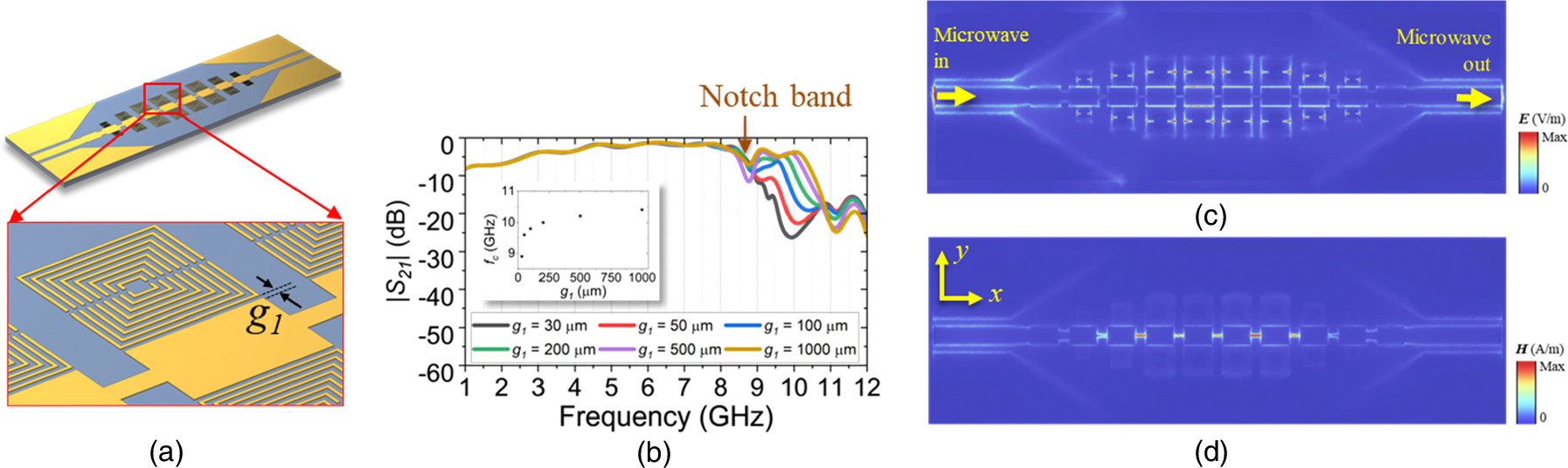
Fig. 4. (a) Illustration of the OFF device consisting of sSPP waveguide capacitively coupled with C-MMs; the inset displays the gap between the stub and the C-MMs (g1 ). (b) Influence of g1 on |S21 | in dB; the inset displays the dependence of the fc on the g1 parameter. (c), (d) Top view distributions of the magnetic field ( H ) and electric field ( E) in the OFF device at a frequency of 6 GHz.
Download figure:
Standard image High-resolution imageAs can be seen from the field confinement in the OFF device, the microwave energy is transferred from the transmission line into the C-MMs by capacitive coupling through an air gap. The influence of g1 on the transmission characteristics was investigated. The simulation results plotted in Fig. 4(b) indicate that the notch band widens to higher frequencies as the g1 parameter decreases. Furthermore, the cutoff frequency decreases when the g1 parameter decreases as shown in the inset of Fig. 4(a). In addition, the transmission band in the frequency range of interest (2–6 GHz) is unchanged when g1 varies. These features were utilized to design the ON device. A metal connector is made in the gap that electrically connects the C-MMs with the stubs to demonstrate phase change between the two delay lines with unchanged transmittance in the target frequency range.
The results of the parametric simulations were employed to determine the dimensions of the fabricated device. These conform to the following conditions: (a) the resonant frequency of the C-MMs is designed so that its resonant frequency is higher than the target frequency range of 2–6 GHz to achieve unchanged transmittance; (b) the device is capable of miniaturization. The parametric simulation results reveal that a wide range of dimensions meet these requirements. In this study, we apply the dimensions listed in Table II of the ON and OFF devices for the next numerical calculation and fabrication of the two delay lines.
Table II. Dimension parameters of the two devices.
| wg | hg | p | g1 |
|---|---|---|---|
| 3 mm | 0.8 mm | 4 mm | 50 μm |
Numerical calculations were performed for the two delay lines with the parameters listed in Table I. The simulated transmission characteristics and phase difference of the ON and the OFF devices plotted in Fig. 5(a) indicate that two simulated transmission bands overlap and a phase difference that is increasingly proportional to frequency in the range of 2–6.5 GHz. The group delay of the two devices was calculated by taking the derivative of phase over frequency (group delay  where φ is phase; ω is frequency) and shown in Fig. 5(b). The calculated group delay or time delay of the OFF device is smaller than that of the ON device in the frequency range of 2–6 GHz. It is deduced that the group velocity of the OFF device is faster than that of the ON device and this explains the phase difference between the two devices in the frequency range of 2–9.2 GHz.
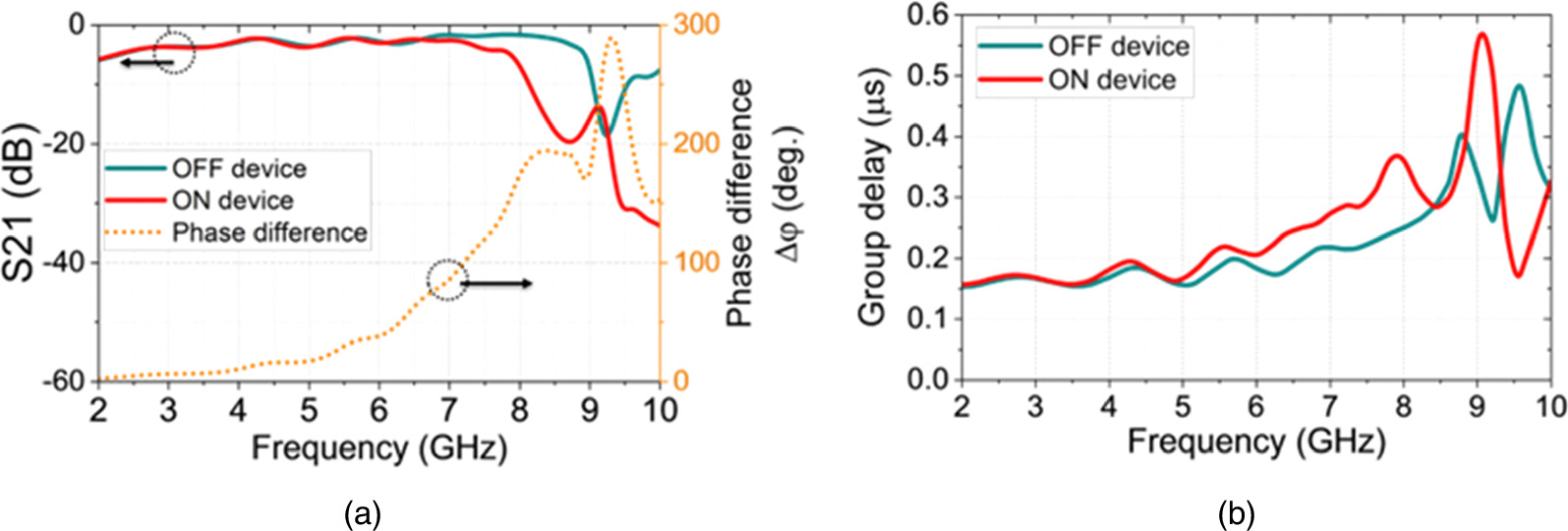
Fig. 5. The simulated transmission characteristics of the ON and OFF devices and the phase difference between the two devices. (b) Group delay of the two delay lines.
Download figure:
Standard image High-resolution imageFor further understanding of the working mechanism of the devices, coupled mode theory (CMT) was taken into qualitative study. CMT is a perturbational method to analyze the coupling of vibrational systems (mechanical, optical, electrical, etc.) in space or in time. Recently, CMT has been applied for the analytical description of resonators coupling via the near-field interaction, more specifically, the coupling between metamaterials and microwave waveguide. 33,34)
We develop from the asymmetric model described in Ref. 35 for the proposed devices which are composed of a sSPP waveguide coupling with symmetric C-MMs on both sides. The CMT model is simplified for one main unit of the delay section with symmetric geometry as shown in Fig. 6(a), wherein a1 , a2 , b1 , b2 are the incoming and reflected coefficient from the two ports; α is to describe the excitation of the C-MMs, so-called positive frequency amplitude, which has magnitude equals the square root of the power stored in a resonant mode, and the argument corresponds to the phase of oscillations. 35)
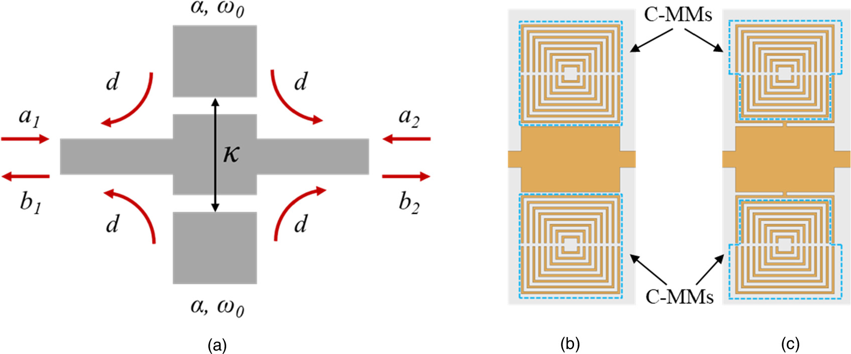
Fig. 6. (a) Schematic of two symmetric resonators edge-coupled to the sSPP waveguide. The structure of the C-MMs group in the main unit of the (b) OFF device and (c) ON device.
Download figure:
Standard image High-resolution imageWhen the coupling between the resonators and sSPP waveguide occurs, there exist two effects: (1) incident waves can excite the resonant modes of the C-MMs; (2) microwave power from resonant modes leaks in the sSPP waveguide. As a result, the S-parameters of the devices are affected by the coupling. The S21 parameter derived from the model in Ref. 35 is as follow:

Wherein, κ is the mutual coupling coefficient between the two C-MMs;  is the resonant frequency of the C-MMs; ω is frequency of the microwave; d1
and d2
are the coupling coefficients due to power leakage from the C-MMs in the sSPP waveguide.
is the resonant frequency of the C-MMs; ω is frequency of the microwave; d1
and d2
are the coupling coefficients due to power leakage from the C-MMs in the sSPP waveguide.  is the S21
of the sSPP waveguide without C-MMs.
is the S21
of the sSPP waveguide without C-MMs.
For the OFF device, there are 16 C-shaped metallic structures in the C-MMs groups. While in the ON device, the stub is connected with one C-shaped metallic structure by a metal connector, then there are only 15 structures left, as can be seen in Figs. 6(b), 6(c), which change the resonant frequency  of the C-MMs, as well as the value of κ,
 d1
, d2
. As a result, from the formula (1), the S21
parameter differs between the ON and OFF devices.
d1
, d2
. As a result, from the formula (1), the S21
parameter differs between the ON and OFF devices.
3. Experimental methods
We fabricated two delay lines consisting of sSPP waveguides and C-MMs on a non-doped silicon substrate (electrical resistivity of 10 000 Ohm·cm) by surface micromachining technologies. The fabrication process is shown in Fig. 7. The substrates were cleaned by using a standard cleaning process in a clean room prior to magnetron sputtering of an 1100 nm Au film. A Cr thin film with a thickness of 40 nm was used as an adhesion layer between the Au thin film with Si substrate. Photolithography was carried out with 405 nm ultraviolet light using one emulsion mask. A photoresist (OFPR800 200 cp) was used for the protection of the wet etching of Cr/Au. The photoresist was spin-coated at 3000 rpm for 20 s before prebaking at 110 °C for 5 min. The exposure dose was 175 mJ cm−2. The development of 2.38% tetramethyl ammonium hydroxide (TMAH) for 100 s was performed before wet etching the Cr/Au thin films. The photoresist was stripped in acetone solution. Finally, the samples were rinsed with deionized water and dried gently under a nitrogen flow.

Fig. 7. The micromachining process for the fabrication of the sSPP waveguides.
Download figure:
Standard image High-resolution imageAfter dicing, each device was bonded with two SMA connectors (RS PRO SMA board end launch connector) by lead-free solder paste (Sn42Bi58 micro-beads) for optical characterization with a vector network analyzer system (E8363C, Agilent Technologies, Ltd.).
4. Results and discussion
Optical images of the fabricated devices are shown in Fig. 8. Figure 8(a) shows the OFF device, which was fabricated on a silicon substrate and bonded with SMA connectors at both ends. Figure 8(b) shows an optical image of the as-fabricated ON device with a metal connector that connects the stubs with the C-MMs. The metal connectors have dimensions of 55 μm × 45 μm, and the fabrication error is determined to be 5 μm due to over-etching of 2.5 μm on two opposite edges of the metal structures. The thickness of the Cr/Au metal on the waveguide during the fabrication process is 1100 nm, which is much thinner than the copper plating formed on conventional RF PCB substrates which is typically 35 μm. Such a thickness is advantageous for miniaturizing structures in metal patterning in the fabrication of common 5G/6G communication devices with low loss, as device pattern dimensions will decrease when signal frequencies increase toward future 6G communications.

Fig. 8. Optical images of the fabricated devices with bonded SMA connectors: (a) the OFF device and (b) the ON device.
Download figure:
Standard image High-resolution imageFigure 9(a) shows the experimental results of the magnitude of the transmission parameter (|S21 |) in dB for the ON and OFF devices in the frequency range from 2 to 10 GHz. The transmission curves of the two devices are almost identical in the frequency range from 2 to 6 GHz. In the ON device, the cutoff frequency is shifted to a lower frequency of 6.91 GHz than that in the OFF device, which is 8.74 GHz. The cutoff frequency shift is the cause of the phase difference between the ON and OFF devices. Figure 9(b) compares the phase difference between the ON and OFF devices (Δφ = φOFF − φON) for the experimental and simulated results, which shows agreement in the frequency range of 2–6 GHz. The measurement results show that the phase difference increases proportionally to a microwave frequency of 2–9.2 GHz. Particularly, in the frequency range of 2–6 GHz, and a phase difference of several tens of degrees is obtained with a small change in the |S21 | between the ON and OFF devices. At 6 GHz, the phase difference is 68° without changing the transmittance (the transmittance is calculated by |S21 |2). At 7 GHz, |S21 | decreases slightly, and the phase difference is 195°. At frequencies higher than 7 GHz, there exists a larger phase difference, and the transmittance also changes significantly.
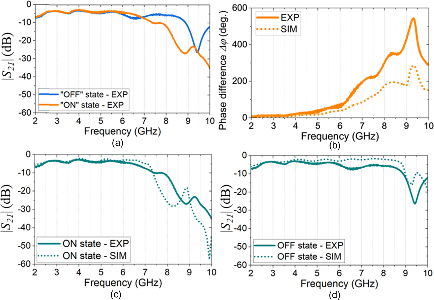
Fig. 9. (a) Experimental results of the |S21 | parameter in dB of the ON and OFF devices. (b) The phase difference between the ON and OFF devices for the experimental and simulated results. Comparison of the |S21 | parameters for the (c) ON and (d) OFF devices.
Download figure:
Standard image High-resolution imageFigures 9(c) and 9(d) compare |S21| between the experimental and simulation results for the ON and OFF devices, respectively. These results indicate that the experimental measurements agree with the numerical calculations in the frequency range of 2–6 GHz. However, at HF, the measured |S21| is lower than the simulated |S21|. These differences can be explained that the skin depth effect and a constant dielectric loss were not considered in the numerical calculation. The dielectric loss is a function of frequency, and it becomes significant in the HF range. In addition, there are other types of loss, such as conductor loss and radiation loss. 36) These losses have not been included in the simulation model due to a lack of experimental data affecting the attenuation mechanism in the microwave range.
The experimental group delay shown in Fig. 10(a) confirms for the simulation in Fig. 5(b) that the time delay for the microwave signal to pass through the OFF device is shorter than that in the ON device in the frequency range of 2–9.3 GHz. Time delay is defined as the time that it takes for the microwave signal to get through the device, which is given by the group delay. The trendlines of the simulated group delay of the ON and OFF devices shown in Figs. 10(b), 10(c), respectively agree with the experimental data.
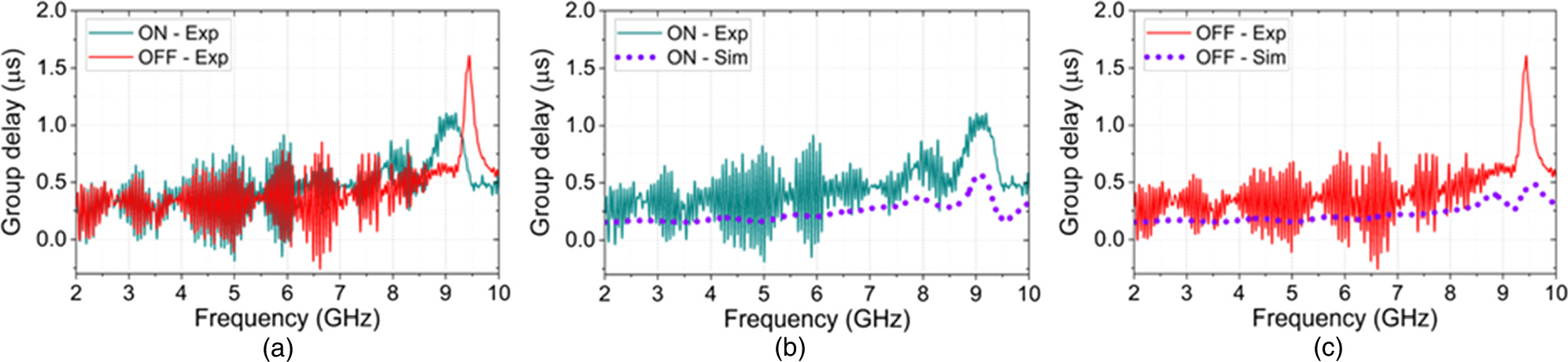
Fig. 10. (a) Experimental group delay of the two delay lines. Experimental and simulated group delay of (b) the ON device and (c) the OFF device.
Download figure:
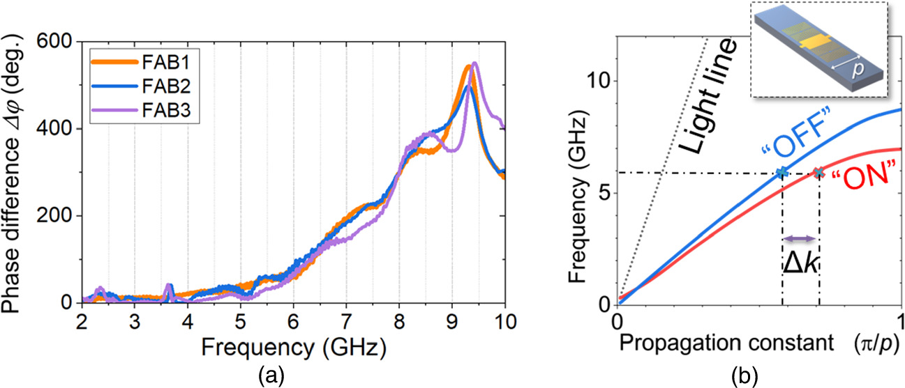
Standard image High-resolution imageThe reproducibility of the device fabrication was also investigated. To confirm the phase difference between the two delay lines, the measurements were repeated on different fabrication batches. The measured results in Fig. 11(a) show a similar dependence between the phase difference and frequency for different fabrication batches, namely FAB1, FAB2, and FAB3. The phase difference between the ON and OFF devices is explained by the nonlinear dispersion relations of the sSPP waves propagating through the devices.
8,9,37) The simulated result using eigenfrequency analysis shown in Fig. 11(b) also indicates that the phase difference between the ON and OFF devices is caused by the dispersion relationship due to the existence of surface plasmon polaritons.
38) Compared to light propagation in free space [the light line in Fig. 11(b)], microwaves propagate with a slower phase velocity in the waveguide.
39) Similarly, the sSPP mode microwave in the OFF device has a faster phase velocity than that in the ON device. The phase velocity is calculated by the formula vp
=  where f is the frequency of the electromagnetic wave and k is the propagation constant. As a result, a phase difference arises between the ON and OFF devices. The observed relationship between the phase difference and frequency occurs due to the different dispersion relationships of the sSPP modes of microwaves propagating through the two delay lines.
Fig. 11. (a) The phase difference between the ON and OFF devices for different fabrication batches. (b) Simulated dispersion relation of the ON and OFF devices; Δk is the propagation constant difference between the ON and OFF devices; the inset is one main unit (p: pitch between the two main units) of the sSPP waveguide with C-MMs.
Download figure:
Standard image High-resolution image
The relationship wherein the phase difference increases approximately linearly with frequency in the range of 2 to 6 GHz can be explained by the ON and OFF dispersion curves with linear characteristics slopes, as shown in Fig. 11(b). Based on the experimental and simulated results, by designing the resonant frequency of C-MMs far from the frequency range of 2–6 GHz and tuning electrical conduction in the gap between the C-MMs and the transmission line, the desired phase difference between the two delay lines can be realized while still maintaining the original transmittance properties.
Recently, the development of phase control devices has raised the need for the integration of metamaterials on the sSPP waveguides for further controlling electrical length for application in phase shifters. 22,23,40) Ye et al. realized a phase shifter with metamaterials that switches between ON and OFF states by changing the electrical conductivity. 24) Gao et al. demonstrated a phase shifter with metamaterials that switches between on and off states by changing the capacitance. 41) However, a large phase difference occurs at the resonant frequency of the metamaterials, resulting in a considerable change in transmittance. With the two delay lines demonstrated in this study, by using a electrical switch, such as MEMS cantilever, micro-bridges or semiconductors diodes, between the metallic stubs of the sSPP waveguide and the C-MMs, a phase shifter or a modulator could be realized with a small change in transmittance.
5. Conclusions
We fabricated two delay lines consisting of sSPP waveguides and C-shaped metamaterials using surface micromachining technology. A novel C-shaped metamaterial was integrated with the sSPP waveguide on a non-doped silicon substrate. Two types of delay lines, namely ON and OFF, were designed and fabricated. The two delay lines resulted in a phase difference of several tens of degrees that maintains the original transmittance in the frequency range of 2–6 GHz. For example, we obtained a phase difference of 68° at a frequency of 6 GHz. This present characterization of delay lines is the first step toward realizing the phase shifter and phase modulation of microwave on one sSPP waveguide using electrical switches, which will be addressed in future work.
Acknowledgments
The authors thank Dr. Satoshi Tomita and Dr. Seigo Ohno for their useful discussion. Part of this work was supported by JST, CREST Grant No. JPMJCR2102, Japan, and was performed at the Micro/Nano-machining Research and Education Center (MNC), Tohoku University, Japan.