

Abstract
In this work, effects of structural parameter scaling on IGBT performance were systematically studied for both 1200 V non-scaled (k = 1) and scaled (k = 3) IGBTs. Relatively small area IGBT test devices with varied device parameters were fabricated on 3 inch wafers simultaneously with full size IGBTs. Mesa width, trench depth, p-base depth (MOS channel length) and gate oxide thickness were varied to clarify the contribution of each scaling parameter. P-collector dose was also varied for both k = 1 and k = 3 IGBTs to control the on-sate voltage. Clear on-state voltage improvement was verified in scaled IGBTs, in agreement with TCAD simulations. The origin of the performance improvement and the possibility of further improvement by scaling are discussed.
Export citation and abstract BibTeX RIS
1. Introduction
As the worldwide electric power demand is rapidly increasing, developments of high efficiency power electronics are important.1–4) While many power devices with wide bandgap materials, such as SiC, GaN, and Ga2O3, are being developed,5–9) Si-IGBTs (insulated gate bipolar transistors) are still the main stream power switching devices and are making steady progress by various new technologies.10–24) The recently proposed three-dimensional scaling concept is one of the effective ways to enhance the Si-IGBT performance.25) In the scaling concept, similarly to the CMOS scaling, all the geometrical dimensions as well as gate voltage are scaled down proportionately while keeping the cell pitch W constant, as shown in Fig. 1.

Fig. 1. (Color online) Scaling principle of trench gate IGBTs.
Download figure:
Standard image High-resolution imageIn our previous study, we have demonstrated both improved on-stage voltage (Vcesat) and reduced turn-off loss (Eoff) in 1200 V-10 A class scaled IGBTs26) designed based on the scaling concept.27) The full size 10A-class IGBT chips had 5 mm2 of active emitter area,26) which was large enough to attain 10 A class on-current. However, since the comparisons were made only between non-scaled and scaled IGBTs where multiple structural parameters are changed at the same time, details of the effects of individual scaling parameters remained unclear and the origin of the improved performance should be made clearer. For this purpose, smaller area IGBT test devices (0.144 mm2 active emitter area) with a wider variety of combinations of the device parameters were fabricated and their on-state voltage drop (Vcesat) was systematically evaluated.28) This paper describes the work in28) in more detail, and provides additional data on the parameter dependence.
2. Device design and fabrication
In the scaling concept for Si-IGBTs (Fig. 1), all the geometrical dimensions of the trench region, i.e. mesa width (S), trench depth (DT), p-base depth (DP) and gate oxide thickness (tox), are scaled down proportionally by a factor of 1/k, while keeping the cell pitch (W) constant, where k is the scaling factor. According to the reduction of the gate oxide thickness, gate voltage is also decreased from 15 to 5 V. The gate voltage reduction will drastically reduce the gate drive power by 1/9, considering that the gate capacitance is kept constant. Although the gate voltage reduction may increase the risk of switching failure, we have already demonstrated 5 V driven turn-off switching without noticeable degradation of the 1200 V 10 A-class IGBTs.26)
Figure 2 shows a photograph of the 1200 V IGBT chips fabricated on a 3 inch wafer. In addition to the 10 A-class main chips, test element group (TEG) chips were prepared, each containing 16 smaller area test IGBTs.29,30) These TEG chip IGBTs consist of 9 pairs of trench gates whose length is 1 mm (active emitter area: 0.144 mm2), with 6 pairs of dummy trench gates on both sides (Fig. 3). The reduce size makes it possible to fabricate a wide variety of IGBTs with different layout design on the same chip. Though a p-float and n-stop pads are provided, which are connected to the p-float and n-base regions (see Fig. 1) at the perimeter of the device, these terminals were not used and kept floated.

Fig. 2. (Color online) Chip photograph of IGBT wafer fabricated in facilities of the Univ. of Tokyo.
Download figure:
Standard image High-resolution image
Fig. 3. (Color online) Photograph and layout of TEG chip.
Download figure:
Standard image High-resolution imageTable I shows the design of experiment (DOE) for this work. "1/3" and "1" in the table indicate whether the parameter is scaled by 1/3 or not. The devices labeled k = 1 and k = 3 are reference non-scaled and fully scaled IGBTs, respectively. Note that while W and S are determined by the layout, DT, DP and tOX are changed by process conditions. A group of parameters related to the MOS gated region DP, tox and Vg are always changed simultaneously. In addition to these structural parameters, p-collector dose was also varied. As a result, 14 types of devices were fabricated in total, as shown in Table I. Figure 4 graphically illustrates the DOE in Table I. The parameter values of designed structure and doping concentration for k = 1 (device A) and k = 3 (device F) are listed in Table II.
Table I. Structural parameters and sample labels of scaled IGBTs.
| NO scaling (k = 1) |

|
Full scaling (k = 3) | |||||
|---|---|---|---|---|---|---|---|
| Cell pitch, W | 1 | 1 | 1 | 1 | 1 | 1 | |
| Mese width, S | 1 | 1/3 | 1 | 1/3 | 1 | 1/3 | |
| Trench depth, DT | 1 | 1 | 1 | 1 | 1/3 | 1/3 | |
| p-base depth, DP | 1 | 1 | 1/3 | 1/3 | 1/3 | 1/3 | |
| Gate oxide thickness, tox | |||||||
| Gate voltage, Vg | |||||||
| Sample labels | |||||||
| ×1/2 | A− | B− | E− | F− | |||
| P-collector dose | ×1(typ.) | A | B | C | D | E | F |
| ×2 | A+ | B+ | E+ | F+ | |||
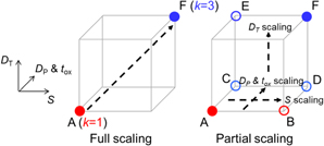
Fig. 4. (Color online) Comparison of diagrams for full scaling and partial scaling.
Download figure:
Standard image High-resolution imageTable II. Designed structure and doping concentration for k = 1 and k = 3 IGBTs.
| k = 1(A) | k = 3(F) | |
|---|---|---|
| W(μm) | 16 | |
| S(μm) | 3 | 1 |
| DT(μm) | 6 | 2 |
| DP(μm) | 3 | 1 |
| Trench width, WT(μm) | 1 | |
| tox(nm) | 100 | 33 |
| Vg(V) | 15 | 5 |
| tsi(μm)a) | 120 | |
| Doping concentration | ||
| Np-base_peak(cm−3) | 1.5 × 10¹⁷ | 1.8 × 10¹⁷ |
| Nn-base(cm−3) | 1.7 × 10¹⁷ | |
| Nn-buffer(cm−3) | 8 × 10¹³ | |
| Np-collector_typ.(cm−3) | 8 × 10¹⁷ | |
3. Device characteristics
Figure 5 shows simulated carrier distributions for the k = 1 and k = 3 devices for the same p-collector doping of 8.0 × 1017 cm−3 when a collector-emitter current density Jce of 200 A cm−2 is flowing. Other parameters of thickness and doping concentration are shown in the figure. It can be seen that, by scaling the device from k = 1 to k = 3, the front side carrier concentration can be selectively increased by the injection enhancement (IE) effect.31) On the other hand, the backside carrier concentration, which is primarily determined by the backside device design including the p-collector doping, is not much changed. Therefore, it is expected that the k = 3 device can decrease the Vcesat without degrading turn-off loss, which is closely correlated with the on-state carrier concentration near the back side of the n-base region.
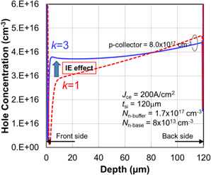
Fig. 5. (Color online) Simulated carrier distribution on k = 1 and k = 3 IGBTs.
Download figure:
Standard image High-resolution imageFigure 6 compares Jce–Vce characteristics of main chip IGBT and TEG chip IGBT for both k = 1 and k = 3 devices. The Vcesat in the TEG chips are significantly reduced from the main chips for both k = 1 and k = 3 IGBTs. This can be explained by the fact that the p-float region of the main chips are weakly connected to ground for stable switching operations.26) By connecting the p-floating region to ground, though the switching stability is improved, the IE effect is weakened due to increased hole sinking via the p-float region, and the Vcesat is increased. Since the IE effect is sensitive to the p-float grounding condition, in this work, the p-float terminal was floated for the TEG chip measurements to avoid complication. Figure 7 compares Jce–Vce characteristics of the TEG chip IGBTs with the TCAD simulation results corresponding to Fig. 5. The p-float regions are fully floated in both cases. Good agreement was confirmed. The scaling from k = 1 to k = 3 reduced the Vcesat defined at Jce = 200 A cm−2 by 0.14 V.

Fig. 6. (Color online) Comparison of on-state characteristics of k = 1 and k = 3 IGBTs on TEG chips and main chips.
Download figure:
Standard image High-resolution image
Fig. 7. (Color online) Simulated and measured (main chip) on-state characteristics of 1200 V k = 1 and k = 3 trench gate IGBTs.
Download figure:
Standard image High-resolution imageMeasured collector-emitter current versus gate-emitter voltage (Ice–Vge) characteristics of the TEG chip devices listed in Table I are shown Fig. 8. The k = 1 group (A−, A, A+, B−, B, B+, MOS gated region is not scaled) and the k = 3 (E−, E, E+, F−, F, F+, MOS gated region is scaled) group devices (see Table I) respectively show almost identical curves irrespective of mesa width, trench depth, and p-collector dose. Threshold voltages (Vth) of the k = 3 group are adjusted to 1/3 that of the k = 1 group by reducing the gate oxide thickness and controlling the p-base doping concentration. The transconductance for the k = 3 group devices was improved by the gate oxide scaling. Figure 9 shows histograms of Vth for the k = 1 group and k = 3 group IGBTs where Vth is defined at Jce = 2 A cm−2. Thanks to the scaled gate oxide thickness, the k = 3 group device exhibit reduced Vth variability.
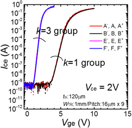
Fig. 8. (Color online) Ice–Vge characteristics of k = 1 group and k = 3 group IGBTs.
Download figure:
Standard image High-resolution image
Fig. 9. (Color online) Threshold voltage distribution of k = 1 group and k = 3 group IGBTs.
Download figure:
Standard image High-resolution imageIt is considered that changing the design parameters will affect IGBT performance in multiple ways as shown in Table III. Mesa width S and trench depth DT will affect both IE effect and parasitic resistance in opposite ways. Narrower mesa and deeper trench will enhance the IE effect through the increase of hole accumulation, but increase parasitic resistance in the n-mesa region (i.e. between the p-base bottom and the trench bottom). Reduction of p-base depth DP will reduce the n-channel resistance of trench gate region. Though the cell pitch W will also affect the performance in multiple ways, it was not changed in the scaling. Because the impact of W is less than other parameters, and optimum point of k = 1 and k = 3 is almost same.25) The improved Vcesat by the scaling (Fig. 7) is considered to be caused by the combination of these effects excluding those related to W. The DOE in Table I and Fig. 4 makes it possible to experimentally examine the various effects shown in Table III separately.
Table III. Impact on IGBT performance by changing design parameters.
| Scaling parameters | Impact on IGBT performance | ||
|---|---|---|---|
| IE effect | N-channel resistance | N-mesa resistance | |
| Narrower Cell pitch (W) | Degrade | Improve | |
| Narrower mesa width (S) | Improve | No effect | Degrade |
| Shallower trench depth (DT) | Degrade | No effect | Improve |
| Shorter p-base depth, Dp | |||
| Thinner gate oxide thickness (tox) | No effect | Improve | No effect |
| Lower gate voltage (Vg) | |||
Figure 10 shows the impact of mesa width change for both k = 1 (A) and k = 3 (F) IGBTs. One trend of recent IGBT development is narrowing of the mesa width32–36) for enhancing IE effect. However, Fig. 10 suggests that the performance improvement by further narrowing the mesa in non-scaled IGBT is limited. On the other hand, mesa width dependence of the scaled IGBTs, whose trench depth is shallower and MOS channel is shorter, is larger than that of the non-scaled IGBTs.

Fig. 10. (Color online) Mesa width dependence of Jce (Ice)–Vce characteristics of (a) k = 1 and (b) k = 3 IGBTs.
Download figure:
Standard image High-resolution imageFigure 11 shows the transition from device A (k = 1) to device E through device C. In device C, only MOS gated region (p-base depth and gate oxide thickness) was scaled from device A, whereas mesa width and trench depth are kept the same. In this case, reduction of the MOS channel resistance is considered to be the main contributor to the Vcesat reduction. In device E, trench depth was scaled from device C while keeping the same mesa width. The Vcesat was degraded due to reduced IE effect in this direction. Figure 12 shows the transition from device B to device F (k = 3) through device D. Similarly to Fig. 11, the Vcesat was improved from device B to D. On the other hand, unlike Fig. 11, it can be seen that the increase of the Vcesat from device D to F is almost suppressed. This suggest that reduced IE effect is effectively compensated by the reduction of n-mesa resistance.
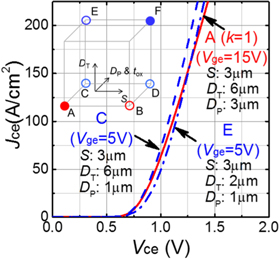
Fig. 11. (Color online) Transition of Jce (Ice)–Vce characteristics with p-base depth and trench depth reduction on 3 μm mesa IGBTs.
Download figure:
Standard image High-resolution image
Fig. 12. (Color online) Transition of Jce (Ice)–Vce characteristics with p-base depth and trench depth reduction on 1 μm mesa IGBTs.
Download figure:
Standard image High-resolution imageFigure 13 summarizes the Vcesat change from device A (k = 1) to device F (k = 3) through partial scaling (device B– E). Starting from device A, narrowing mesa width (A–B) and shortening the p-base depth (A–C) achieved Vcesat reduction, which were attributed to enhanced IE effect and reduced channel resistance, respectively. Combination of these two can realize further reduction of the Vcesat (A–D). According to the proposed scaling rule, the trench depth should be also scaled down proportionally with the gate oxide thickness, since the gate capacitance has to be kept constant. Though this will suppress IE effect (C–E), this negative impact was compensated by reduced parasitic resistance for the case of D–F. As already pointed out referring to Fig. 10, narrowing the mesa from E–F achieves much larger improvement than A–B. This suggests that the proposed scaling rule that include vertical scaling can enlarge the room for optimization.
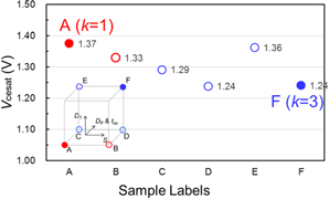
Fig. 13. (Color online) Comparison of Vcesat of non-scaled, fully scaled and partial scaled IGBTs.
Download figure:
Standard image High-resolution imageNext, the dependence on back side p-collector dose of Jce–Vce curves for both non-scaled and fully scaled IGBTs are shown in Fig. 14. It was found that Vcesat improves with p-collector dose more in k = 3 than k = 1. As is well known, Vcesat can be controlled by simply changing the p-collector dose. However, if the p-collector dose is increased to reduce Vcesat, the on-state carrier concentration in the n-base region, particularly near the back side, is increased, and the switching loss is degraded. Therefore, it is important to achieve low Vcesat, while keeping the back side doping as low as possible. One advantage of scaled IGBTs is the higher on-state carrier concentration near the front side, as was shown in Fig. 5, which is beneficial for lowering Vcesat without increasing the back side doping. In addition to this, Fig. 14 shows that scaled IGBTs will have higher controllability of Vcesat, which will be beneficial for device optimization.

Fig. 14. (Color online) The p-collector dose dependence of Ice (Jce)–Vce characteristics of (a) k = 1 and (b) k = 3 IGBTs.
Download figure:
Standard image High-resolution imageMeasured dependences of Vcesat on P-collector does are summarized in Fig. 15. It can be confirmed that Vcesat of the k = 3 devices show larger sensitivity to not only the mesa width but also p-collector doping. The results suggest again that the proposed scaling can enlarge the possibility of performance improvement than simple mesa width scaling.

Fig. 15. (Color online) Comparison of Vcesat of k = 1 group and k = 3 group IGBTs with varied p-collector dose for different mesa width.
Download figure:
Standard image High-resolution image
4. Conclusions
Structural parameter dependence of 1200 V IGBT Jce–Vce characteristics was systematically studied in order to explore the possibility of further performance improvement by the parameter scaling. Measurements without complication by p-float grounding were achieved using small scale IGBT test devices. It was confirmed that both MOS channel resistance reduction and increased IE effect are responsible for the improved Vcesat of the scaled devices. It was also found that the scaled devices show larger dependence of Vcesat on p-collector dose and mesa width. This suggests that IGBT scaling will be effective for enlarging the design space to achieve better performance.
Acknowledgments
The authors would like to thank K. Sato of Mitsubishi Electric Corp., Dr. T. Matsudai of Toshiba Electronic Devices & Storage Corp., Dr. M. Tsukuda of Green Electronics Research Institute, and Prof. W. Saito of Kyushu University for fruitful discussions. This work is based on results obtained from a project commissioned by the New Energy and Industrial Technology Development Organization (NEDO).