
Computational Investigation of Advanced Refractive Index Sensor Using 3-Dimensional Metamaterial Based Nanoantenna Array


School of Science and Technology, City University of London, London EC1V 0HB, UK
*
Author to whom correspondence should be addressed.
Sensors 2023, 23(3), 1290; https://doi.org/10.3390/s23031290
Submission received: 17 October 2022
/
Revised: 18 January 2023
/
Accepted: 21 January 2023
/
Published: 23 January 2023
(This article belongs to the Special Issue Selected Papers from the 5th International Conference on Applications of Optics and Photonics (AOP2022))
Abstract
:Photonic researchers are increasingly exploiting nanotechnology due to the development of numerous prevalent nanosized manufacturing technologies, which has enabled novel shape-optimized nanostructures to be manufactured and investigated. Hybrid nanostructures that integrate dielectric resonators with plasmonic nanostructures are also offering new opportunities. In this work, we have explored a hybrid coupled nano-structured antenna with stacked multilayer lithium tantalate (LiTaO3) and Aluminum oxide (Al2O3), operating at wavelength ranging from 400 nm to 2000 nm. Here, the sensitivity response has been explored of these nano-structured hybrid arrays. It shows a strong electromagnetic confinement in the separation gap (g) of the dimers due to strong surface plasmon resonance (SPR). The influences of the structural dimensions have been investigated to optimize the sensitivity. The designed hybrid coupled nanostructure with the combination of 10 layers of gold (Au) and Lithium tantalate (LiTaO3) or Aluminum oxide (Al2O3) (five layers each) having height, h1 = h2 = 10 nm exhibits 730 and 660 nm/RIU sensitivity, respectively. The sensitivity of the proposed hybrid nanostructure has been compared with a single metallic (only gold) elliptical paired nanostructure. Depending on these findings, we demonstrated that a roughly two-fold increase in the sensitivity (S) can be obtained by utilizing a hybrid coupled nanostructure compared to an identical nanostructure, which competes with traditional sensors of the same height, (h). Our innovative novel plasmonic hybrid nanostructures provide a framework for developing plasmonic nanostructures for use in various sensing applications.
1. Introduction
Researchers have become more interested in surface plasmon polaritons (SPPs), since they can provide fresh, remarkable opportunities for the future era of nanotechnologies. Due to the advancement of semiconductor fabrication techniques and electron beam lithography, researchers have lately delved into the manufacture of nano-antennas [1], which range in size from a few hundreds of nanometers to over several microns. To construct effective nano photonic devices [1] with ultra-fast operational speed and the capability to concentrate the electromagnetic field into a region which is significantly narrower than the operating wavelength [2], using SPPs ensures that the objectives of the nanophotonic branch [3] are addressed. SPPs have been used extensively in several technologies, including waveguides [4], modulators [5], nano-lasers [6], nano rings [7], nano wires [8] and nano-antennas [9]. These can be advantageous because of their rapid transient response, compactness, and adjustability in efficiency parameters. However, since metal is dispersive in the visible spectrum, so it must be simulated with an accurate dielectric permittivity function [10,11,12,13,14,15]. Yousafi et al. [16] have suggested a rectangular patch nanostructure to radiate the localized electromagnetic wave power of the hybrid plasmonic waveguide [17,18,19] in which the electromagnetic waves were contained in thin material having very low refractive index in between plasmonic metallic layers. Another purpose of using a hybrid nano antenna system is to achieve the high propagation length. In the traditional single nano antenna system, low efficiency has been seen due to their significant ohmic losses [20,21,22]. To avoid this drawback, a hybrid nano antenna is proposed, which can enhance the performance of the antenna system by reducing the ohmic losses [23,24,25,26]. The separation distance also [27,28,29] plays an important role in enhancing the applied electric field for plasmonic nanostructures [30,31,32,33,34,35,36,37,38,39,40,41,42]. By using the coupled hybrid structure, the electric field confinement can be enhanced and reduce the ohmic losses by using dielectrics (having large refractive index) [43,44,45]. Several studies have been presented to support these arguments using meta-surfaces [46,47], meta-materials [48], architectural color combinations [49], and optical nano antennae [50,51,52,53]. Dielectric and metallic nanostructure combinations have been demonstrated to be able to alter the linear and non-linear far field behaviors of paired structures [54,55,56,57,58,59], in addition to the fact that they emit radio frequencies to work as antennas [60,61]. Recently, in terms of sensitivity, there have been several reports of biosensors using artificially created metamaterials. In 2009, Kabashin et al. reported [62] a sensitivity of 30,000 nm/RIU for two-dimensional porous gold nanorod arrays on a plasmonic hyperbolic metamaterial for biosensor applications. However, despite being miniaturized for commercial biosensing applications, this bulk Kretschmann arrangement is not suitable for more compact integrated photonic sensors. Subsequently, in 2016, Sreekanth et al. [63] reported a similar sensitivity of 30,000 nm/RIU for a grating coupled hyperbolic metamaterial for bulk refractive sensing. However, in the presented work we report on a planar optic design, suggesting good sensitivity which can be more compact, and potentially of lower cost when mass produced.
In this paper, we have proposed a novel hybrid lithium tantalate (LiTaO3) or aluminum oxide (Al2O3) multilayer stacked elliptical paired nanoantenna. These materials are more widely available, less toxic, and thus more appropriate for biological/medical applications. In the case of LiTaO3, the magnitude of the spontaneous polarization changes the temperature and disappears at a critical temperature called the Curie temperature (TC). For LiTaO3, ferroelectrics are of particular interest for biological applications as their TC is very high (680 °C), which is very far from typical operating temperatures in biological applications. Similarly, Al2O3 ceramics are being widely used for medical devices, and their biocompatibility is well known and has been reported in recently published articles. Hence, both of these materials used in the proposed device are bio-compatible and can be used in a variety of biomedical and other sensing applications. Recently published studies of the multilayered hybrid plasmonic antenna, which surpasses prior plasmonic waveguides in terms of confinement and propagation losses [24,25], served as the inspiration for the proposed hybrid nanostructures. Unlike the usually presented local field antenna, our proposed nano structure enables an efficient performance even while retaining a very high intensity in the local field. This paper is divided into four sections, where Section II describes the computational design and optimization methods. Section III evaluates the parametric studies of the multi-layer structure. Section IV discusses the effect of the separation distance on the LiTaO3 and Al2O3 stacked nanostructures. Finally, a conclusion and future possibilities are drawn.
2. Approaches for Computational Design and Optimization
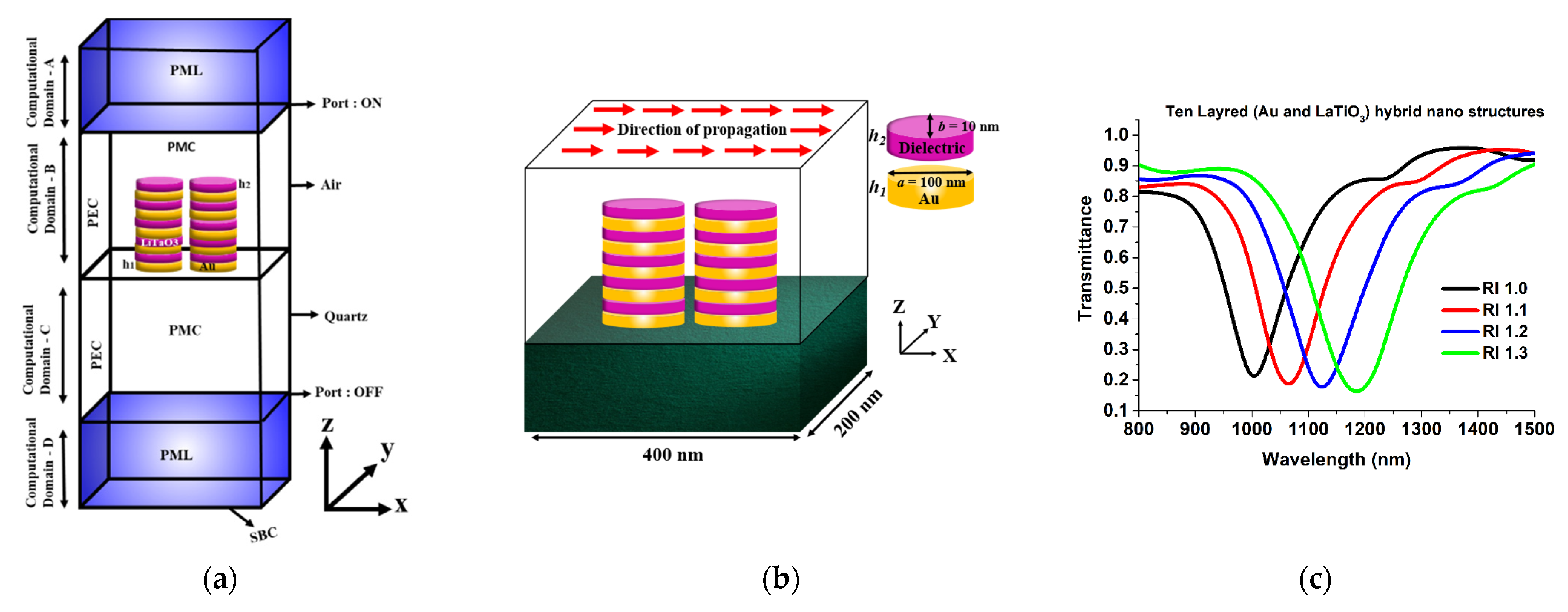
In this paper, the COMSOL Multiphysics software enabled with the finite element method (FEM) in the frequency domain has been used to calculate the plasmonic response and to design the coupled hybrid nano structured antenna, as shown in Figure 1. Figure 1a shows the computational domain, and to reduce the computational time (for designing the whole array of the metamaterial antenna array), we have designed the unit cell and enforced the periodicity in the x and y directions. In the computational domain, the Perfect Magnetic Conductor (PMC) has been used along the x-axis and the Perfect Electric Conductor (PEC) has been employed along the y-axis. By using these boundary conditions, the whole computation walls will act as a mirror and compute the results for the metamaterial antenna array.
To reduce the back reflection, the Perfect Matched Layer (PML) has been used along the z-direction. The quartz substrate has been optimized 400 × 200 nm2 length and width, respectively. A hybrid nano antenna array has been excited by x-polarized light propagating in the z-direction from the top of the antenna array, i.e., the polarization is parallel to the x-axis of the antenna dimer. The final design of the 10 layered hybrid sensor system placed on the 400 × 200 nm2 quartz is shown in Figure 1a. Figure 1b shows a 3D view of the schematic of the designed computational domain of a hybrid nanostructured antenna array. The dielectric properties of gold have been calculated using the Drude-Lorentz model, as it is based on the movement of the unbounded electrons in the metal that causes the surface plasmon resonance. The material properties of Au have been adopted from Johnson et al. [64]. LiTaO3 and Al2O3 are adopted from Moutzouris et al. and Boidin et al. [65], respectively. We have fixed these values in order to make a quick computation, as the height of the source and the substrate did not affect the sensitivity. After we obtained consistent solutions, we have varied the antenna array parameters, and these are only reported here. In this article we have calculated the sensitivity of the paired hybrid nanoantenna array and compared them with a single metallic nano antenna array in the extremely fine mesh size in order to get stable results.
We then explored the sensitivity to variations in the refractive index of the medium of the 10 total layered (with 5 layers of LiTaO3 (or Al2O3) and gold each) stacked elliptical-shaped paired nano structure, with its minor axis, b = 10 nm and major axis, a = 100 nm. Linearly x-polarized electromagnetic waves in the z-direction were used to illuminate these paired nano structures. Through the analysis of transmittance at various refractive index values, its sensitivity has been optimized. Figure 1c displays the transmission spectra for a design specification using various surrounding media (n). Here, the major axis a = 100 nm, minor axis, b =10 nm, separation distance, g = 10 nm and h1 = 10 nm and h2 = 10 nm are selected, as are the LiTaO3 (or Al2O3) and gold (Au) thickness, respectively of the stacked nano structure. Since Figure 1b demonstrates a more effective change in the resonating wavelength, it can be employed as a refractive index sensor and is a good contender for biosensing applications. The spectral absorption of the narrow band paired structures can also be modified to match the distinctive absorption spectra of a certain targeted RI in order to identify the targeted medium inside the infrared range. To calculate the sensitivity, the following equation has been used.
where, λres is the shift in the resonance wavelength and ns is the surrounding refractive index.
3. The Parameterized Investigation of the Multi-Layered Structure
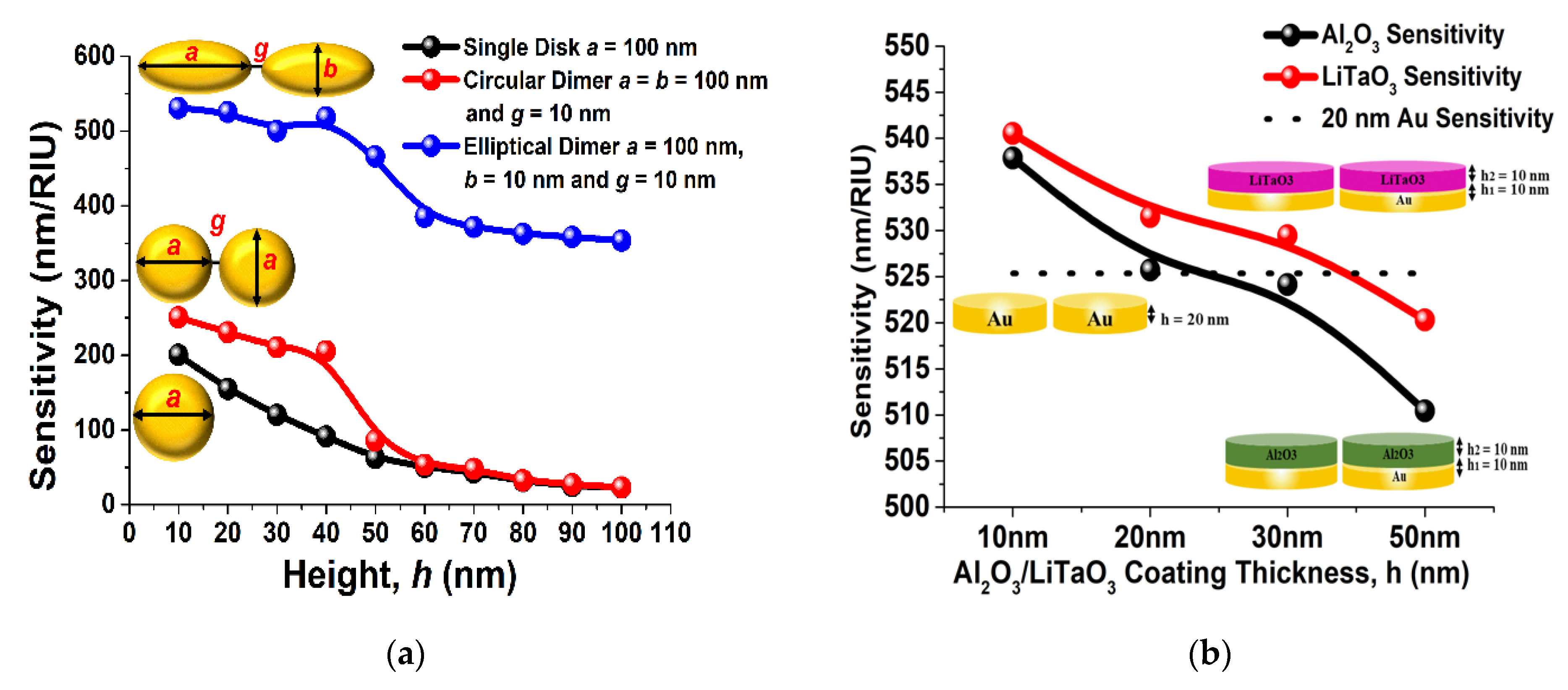
In this section, we have analyzed the performance of a hybrid nano structure and compared it with a single metal nano structure. Figure 2a shows the comparative analysis of sensitivity of the single, paired circular and paired elliptical metallic nano structures. Here, a black curve shows that when h = 100 nm the sensitivity value was nearly 5 nm/RIU and increases as h is reduced, and it reaches nearly 200 nm/RIU when h = 10 nm for a single nano disk. The response of the paired circular nano antenna array when a = b = 100 nm and g = 10 nm is shown by a red curve, and the highest sensitivity of 250 nm/RIU was achieved when h = 10 nm, which sharply increases for lower h values. The sensitivity response of the paired elliptical shaped antenna array is shown by a blue curve when a = 100 nm, b = 10 nm, and g = 10 nm. The blue curve shows the highest sensitivity value of nearly 525 nm/RIU at h = 10 nm and it gradually decreases for higher h values. In all cases, it can be observed that the highest sensitivity of a single metal dimer can be achieved at nearly 525 nm/RIU when its height is reduced to 10 nm. The motivation of selecting the aspect ratio b/a = 1/10 is based on the study reported in a previous manuscript [66].
Verma et al. [66] have shown that as the separation distance, g, decreases, the value of the sensitivity increases, and at g = 10 nm, the highest sensitivity value has been achieved. Additionally, the performance of the symmetry has also been discussed with respect to the separation distance, g. In this work, we will show that the performance can be further improved by placing a layer of LiTaO3 or Al2O3 on top of the metallic paired nano antenna array. Figure 2b shows the sensitivity comparison of the paired gold elliptical shaped antenna array, where the LiTaO3 or Al2O3 has been stacked on the earlier optimized [66] elliptical dimer with a = 100 nm, b = 10 nm, g = 10 nm, and metal thickness h1 = 10 nm. A black dashed curve shows a nearly 523.543 nm/RIU sensitivity of single layer gold elliptical dimer antenna array when h was kept constant at 20 nm. On the other hand, when Al2O3 was placed on the top of the paired elliptical shaped antenna array, the sensitivity increases and reaches up to 532 nm/RIU (shown by the black curve). The values increase even more and reaches up to 543 nm/ RIU (shown by a red curve) for LiTaO3 for h2 = 10 nm. From this it can also be stated that as the height h2, of the LiTaO3 and Al2O3 layer decreases, the sensitivity is increasing. Although it is true that sensitivity increases as the metal or dielectric layer thickness is reduced, getting a very thin layer may bring fabrication uncertainty, and for a fair comparison, the minimum height, h2 of the LiTaO3 and Al2O3 layer is fixed at 10 nm for further observations.
3.1. Performance of the Ten Layered Elliptical Shaped Antenna Array Stacked with Al2O3 and LiTaO3
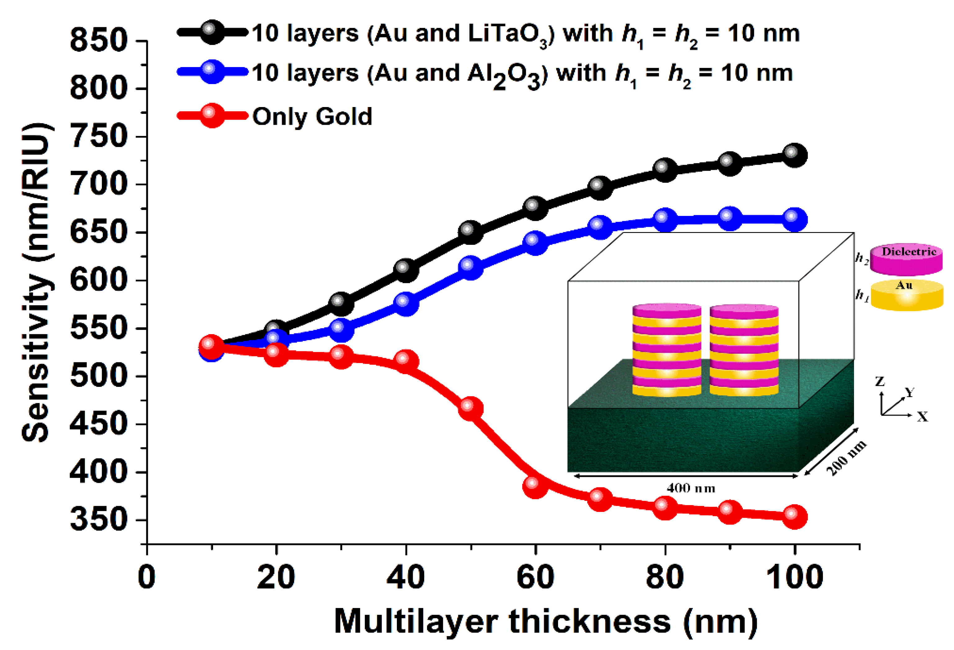
The sensitivity of the stacked antenna array is next evaluated in this section, where we have shown the sensitivity performance of a multiple layered paired elliptical shaped antenna array designed when a = 100 nm, b = 10 nm, g = 10 nm, and h = 100 nm.
The red curve in Figure 3 shows the sensitivity values when height, h, varied from 10 nm to 100 nm for a single metal elliptical dimer. From this figure it can be observed that at a large value of height, h = 100 nm, the sensitivity of the single metal antenna arrays its lowest when a value of nearly 360 nm/RIU was achieved. However, as the height, h is reduced to 10 nm, the sensitivity increases and reaches its highest value of nearly 525 nm/RIU. On the other hand, the blue curve shows that as the number of the layers in the stacked antenna array (with Al2O3) with a = 100 nm, b = 10 nm, g = 10 nm, h1 = 10 nm, and h2 = 10 nm is increasing, the sensitivity rather increases when the height of the stacked layer is increasing and reaches up to its saturation point of nearly 660 nm/RIU. In other words, it can be concluded that by using an Al2O3 stacked antenna array the sensitivity can be enhanced by 1.5 times as compared to a single metallic antenna array keeping h1 fixed at 10 nm. Similarly, the blue curve in Figure 3 demonstrates that by using a 10 layered LiTaO3 stacked antenna array with a = 100 nm, b = 10 nm, g = 10 nm, h1 = 10 nm, and h2 = 10, the sensitivity can be further enhanced by more than two-fold (nearly 730 nm/RIU) as compared to the single gold elliptical paired antenna array. It is worth noting a remarkable more than two-fold increase of the sensitivity and the highest electromagnetic field confinement that has been observed by using the stacked antenna array approach. Hence, such LiTaO3 and Al2O3 stacked plasmonic sensors can detect the small change in the surrounding medium with a sensitivity of about 730 nm/RIU and 660 nm/RIU, respectively, and its sensitivity is expected to increase further by decreasing the height of the individual layers and also the corresponding separation distance.
3.2. Study of Field Distribution around the Single Metal and Ten-Layered (5 Pairs of Gold and LiTaO3 Stacked) Elliptical Shaped Antenna Array
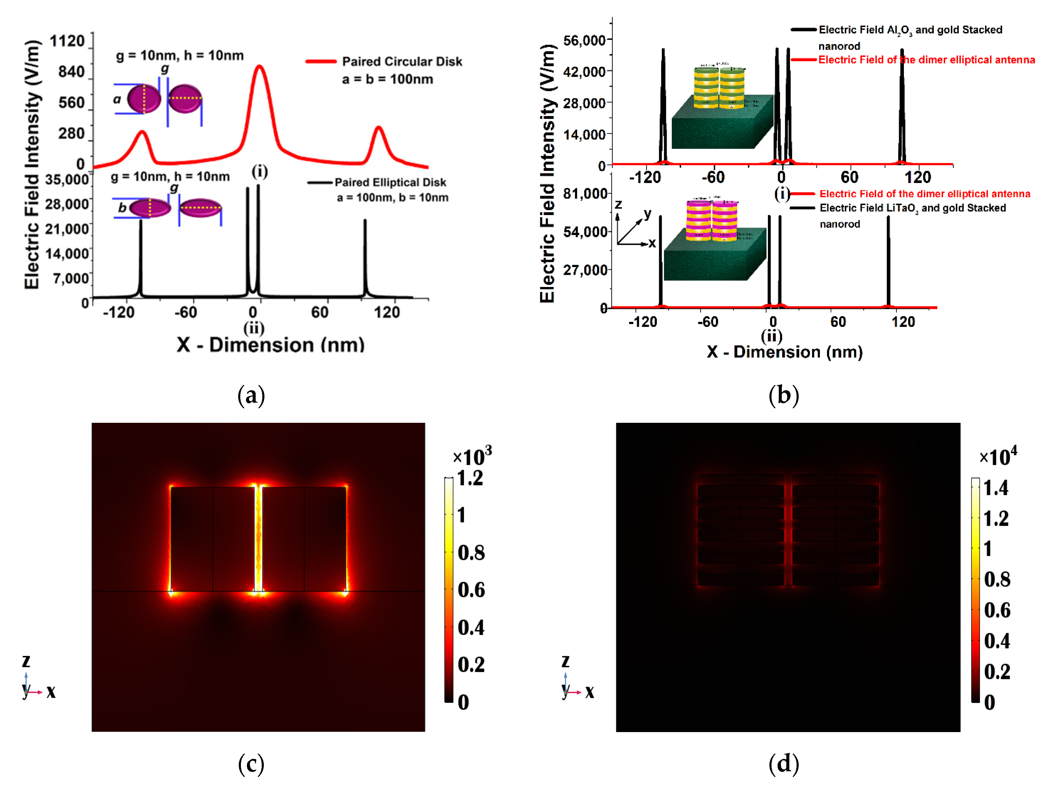
In this section, the performance of the electric field distribution along the single metal and stacked antenna array is discussed. The peak normalized electric field intensity of the single gold circular and elliptical pair was calculated (from COMSOL Multiphysics) as nearly 8.6 × 10² V/m, and 2.9 × 10⁴ V/m reached at the inner edge, as shown in Figure 4a(i) and (ii). It can be noted that the peak fields at the outer edges of the diameter is smaller than the peak field in the gap region. The variation of the electric field, Ex, along the x direction through the center of the single metallic (gold) elliptical nano structure is shown in Figure 4b by a red curve, which is compared with the Al2O3 and LiTaO3 stacked nanostructured field distribution shown by the black curve (shown in Figure 4b(i) and (ii)). In the case of the Al2O3 stacked nano structure, the electric field intensity was calculated nearly 5.4 × 10⁴ V/m, which is nearly nine times higher (shown by a black curve in Figure 4b(i)) than that of the single metallic elliptical-shaped nano structure shown by a black curve. However, the electric field intensity even increases further, up to 6.5 × 10⁴ V/m at the inner edges of the LiTaO3-stacked elliptical nano structure with a = 100 nm, b = 10 nm, and h = 100 nm, as shown by a black curve in Figure 4b(ii). This value is nearly 10.5 times that of a single gold elliptical nano structure, with a = 100 nm, b = 10 nm, and h = 100 nm. In contrast to a single metallic nano structure, the LiTaO3 stacked elliptical nano structure demonstrated in Figure 3 had an improved sensitivity. As a result, it can be regarded as a potential candidate for several bio sensing applications. For single elliptical dimers of height, h = 100 nm, Figure 4c shows the mode profile along the center of the x-z plane, demonstrating where most of the electric field confinement occurs at the sharp corners and in the separation gap between the two elliptical nano structures. As we have considered the elliptical dimer, the higher electric field exists close to the narrower corners, and the variation of Ey along the x-z plane for a single elliptical dimer with h = 100 nm is shown in Figure 4c. This demonstrates that, due to the absence of a circular symmetry, the electric field intensity was more localized near the sharper corners and at four single metal/ dielectric interfaces at the upper, lower and two sides.
The electric field distribution along the center of the x-y plane of the stacked nanostructure is also shown in Figure 4d, where most of the electric field occurs. From there it can be clearly observed that the electric field intensity is higher and localized at all metal/dielectric interfaces, including the 8 inner metal/dielectric interfaces in the stacked nano structure as compared to the single metallic nano structure. The strong electric field enhancement of the electric field provided by the array of antenna array dimers can be used for a surface-enhanced Raman spectroscopy [67,68,69,70]. Figure 5a displays the Ex, mode field pattern along the x-y plane for an elliptical dimer with a height h = 100 nm. It can be observed that the sharp corners and separation gap of the elliptical nanostructure are where most of the electric field confinement occurs. The Ex-field profile has been shown along the x-y plane when z = 100 for the LiTaO3 stacked antenna, as shown in Figure 5b.
This indicates that the field was more concentrated at the corners and at four single metal/dielectric contacts at z = 100 nm, because of the absence of circular symmetry, as shown in Figure 5b. Also, the electric field at z = 0 and 50 nm was calculated as 1.0 × 10² V/m and 1.8 × 10³ V/m, respectively. Hence, from here it can be stated that the stacked antenna array is a more efficient candidate for the sensing application compared to a single metal antenna array, even with the same other structural dimensions.
4. Effect of the Separation Distance on the LiTaO3 and Al2O3 Stacked Nano Structure
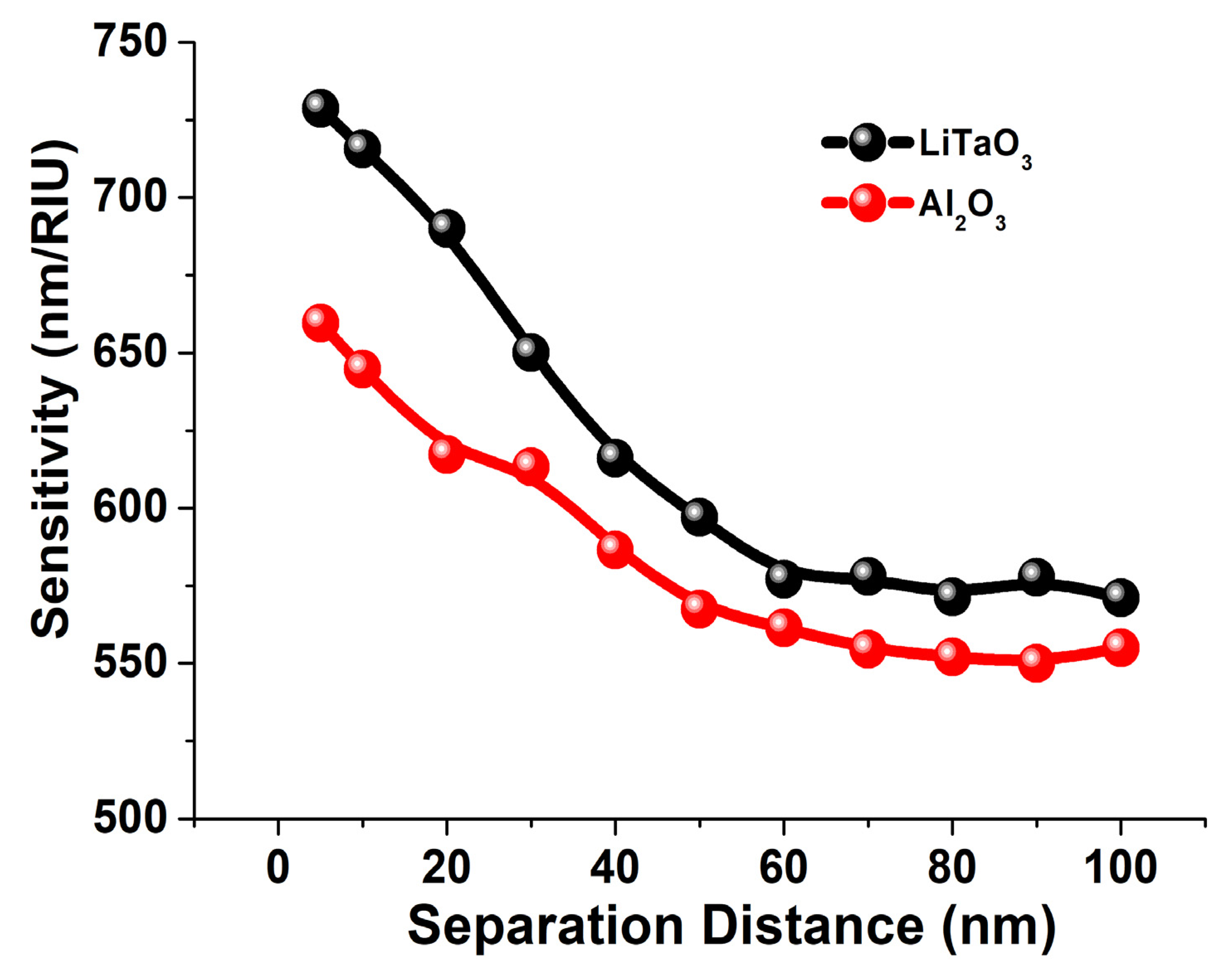
It is well known that the structural dimensions of the nano structures can enhance the field intensity in the separation gaps, and due to this field enhancement the sensitivity can be affected, so next the performance of the 10 layered LaTiO3 and Al2O3 stacked nano structures was studied. Hence, a 10 layer paired elliptical dimer on the quartz crystal was studied and the sensitivity was calculated when the surrounded medium was covered by the different refractive indices from 1.0 to 1.5. Here, it can be noted that, as shown in Figure 1c for a single case, as the refractive index was increasing, the resonating wavelength was shifting towards the higher range. Figure 6 shows the sensitivity of the LiTaO3 and Al2O3 stacked nano structure when the separation distance, g varies from 10 nm to 100 nm. The sensitivity of the 10 layered LiTaO3 stacked paired nanostructure is calculated from the slopes of the shift in the transmission spectra from where we observed the linear relationship between the RI values and the plasmonic wavelengths. The R-square error value was calculated as 0.9991 and 0.9817 for the 10 layered LiTaO3 and Al2O3 stacked paired nanostructure, respectively suggesting an almost linear response. Figure 6. clearly shows that at the separation distance, (g) = 100 nm, the sensitivity reaches 545 nm/RIU, which is effectively the sensitivity of a single isolated layered elliptical dimer. However, when the separation distance, (g) reduced further and reached up to 60 nm, the sensitivity remained nearly constant at 550 nm/RIU. Finally, as the separation distance, (g)reduced further to 10 nm, the sensitivity increases rapidly and reaches up to 660 nm/RIU, as shown by the red curve. Similarly, the sensitivity dependence of the LiTaO3 stacked antenna array with the separation distance is shown by the black curve.
The highest sensitivity of the LiTaO3 stacked antenna array was achieved at nearly 770 nm/RIU when g = 10 nm and reduces gradually with the increase in the separation distance. Finally, after g = 60 nm the sensitivity remained nearly constant, as shown by the black curve, and at g = 100 nm the sensitivity was obtained up to 555 nm/RIU. When the separation distance, g, is higher, these metallic antenna arrays are effectively uncoupled and achieved 555 nm/RIU and 545 nm/RIU sensitivity when they could be considered as two isolated antenna arrays. However, as the separation distance, g is reduced, these two isolated antenna arrays are now coupled, and they formed an effective dimer and their sensitivity reached up to 660 nm/RIU and 770 nm/RIU for the hybrid Al2O3 and LiTaO3 structure, respectively. Thus, it is demonstrated here that the sensitivity of the hybrid LiTaO3 and Al2O3 paired nano structure is always higher than that of a single metallic nano structure. Tsai et al. [71], reported that by using a coupled nano ring, the sensitivity can be enhanced by up to 50%, but our work shows that for an elliptical nano structure using a stacked antenna array nanostructure. The sensitivity values can be further increased by more than 150% while using a much smaller overall size of the antenna array compared to [66]. The change in angle of incidence can produce the TP resonance mode through the reflectance spectrum, and thus we have compared our work with the Tamm sensors shown in Table 1 below.
Hence, this can be an attractive method for detecting the heavy metals, biochemicals, air quality, and water purity, and this is more efficient and cost-effective (if they are fabricated in bulk) and opens up new pathways for both healthcare and environmental monitoring applications. The comparision between the proposed work and the other metallic and hybrid structures are shown in Table 2.
The proposed hybrid nano antenna system has shown very high sensitivity, and this can be enhanced furthermore by using small geometrical dimensions, but we have suggested suitable dimensions which can be experimentally fabricated. There are several lithographic methods that are available to fabricate such small nano structures as those which are mentioned in the literature [72,73,74,75,76,77,78,79,80,81]. We cannot avoid the fact that to design the smaller structure can be challenging; however, the masking method can work well in this scenario. To avoid further experimental complexity, we have used the same dimensions of the gold and dielectric layer. The asset of the proposed sensor is that it can be used as a stand-alone device with the great amount of stability, as we are proposing that the sensing on the substrate and the material used in the sensing device are highly biocompatible and stable so it can be good to consider these kind of sensing devices.
5. Conclusions
In conclusion, we have reported a study of a hybrid (LiTaO3 and Al2O3) stacked metallic nano plasmonic sensor. The designed and optimized sensor with a = 100 nm, b = 10 nm, g = 10 nm, h1 = 10 nm, and h2 = 10 nm has been evaluated in various surrounding refractive indices from 1.0 to 1.5 to calculate their corresponding sensitivity. The transmission, absorption, reflection spectra and modal field profiles have also been calculated to observe the sensor performance. The designed hybrid sensor has been compared with a single metallic nanoantenna array when a = 100 nm, b = 10 nm, g = 10 nm, and h = 100 nm to observe the sensitivity enhancement. From the aforementioned results, it can be stated that the sensitivity can be enhanced by nearly 1.5 times by using an Al2O3 stacked antenna array and by more than two times by using LiTaO3. It has also been shown that the sensitivity can be further increased by reducing the metal height, h1, and the dielectric height, h2, or the separation distance, g. But for a fair comparison, the values of these are taken as 10 nm. The normalized electric field intensity of the LiTaO3 and Al2O3 stacked antenna array were stronger, at nearly 6.5 × 10⁴ V/m and 5.4 × 10⁴ V/m, respectively, which was approximately 10.5 times more than the single metallic nanostructure for LiTaO3 and nine times more than the Al2O3 stacked antenna array. The proposed nano-enhanced antenna’s sensitivity is demonstrated by the use of a full-wave electromagnetic simulation. Our suggested nano-antenna array may be used for different nano inter- and intra-chip photonic sensor systems to develop cutting-edge detecting devices for measuring the quality of water, air, and soils. Furthermore, due of its wide frequency coverage, this suggested antenna array may be employed for biosensing, optical energy harvesting (also known as nano-rectenna (where the top performer rectenna has used oxide/metal bilayer plasmonic antenna [82] or Nantenna and THz Metasurface-mediated nano-biosensors [83]) and various artificial intelligence based [84,85] optical sensing applications.
Author Contributions
Conceptualization and methodology by B.M.A.R.; software handling, validation and original draft preparation by S.V.; All authors have read and agreed to the published version of the manuscript.
Funding
This research received no external funding.
Institutional Review Board Statement
Not applicable.
Informed Consent Statement
Not applicable.
Data Availability Statement
The supporting information can be found from the corresponding author.
Acknowledgments
The authors would like to acknowledge the University of London for providing an excellent infrastructure. This study was supported in part by the University of London Doctoral fellowship Program, and S.V. would also like to acknowledge the worshipful company of scientific instrument makers for contributing partial funds.
Conflicts of Interest
The authors declare that they have no conflict of interest.
References
- Wang, J.J.; Chen, L.; Tai, S.; Deng, X.; Sciortino, P.F.; Deng, J.; Liu, F. Wafer-based nanostructure manufacturing for integrated nano optic devices. J. Light. Technol. 2005, 23, 474. [Google Scholar] [CrossRef]
- Xiong, X.Y.; Jiang, L.J.; Sha, W.E.; Lo, Y.H.; Chew, W.C. Compact nonlinear Yagi-Uda nanoantenna. Sci. Rep. 2016, 6, 18872. [Google Scholar] [CrossRef] [PubMed] [Green Version]
- Thraskias, C.A.; Lallas, E.N.; Neumann, N.; Schares, L.; Offrein, B.J.; Henker, R.; Plettemeier, D.; Ellinger, F.; Leuthold, J.; Tomkos, I. Survey of photonic and plasmonic interconnect technologies for intra-datacenter and high-performance computing communications. IEEE Commun. Surv. Tutor. 2018, 20, 2758–2783. [Google Scholar] [CrossRef] [Green Version]
- Guo, J.; Li, J.; Liu, C.; Yin, Y.; Wang, W.; Ni, Z.; Fu, Z.; Yu, H.; Xu, Y.; Shi, Y.; et al. High-performance silicon−graphene hybrid plasmonic waveguide photodetectors beyond 1.55 μm. Light Sci. Appl. 2020, 9, 29. [Google Scholar] [CrossRef] [Green Version]
- Klein, M.; Badada, B.H.; Binder, R.; Alfrey, A.; McKie, M.; Koehler, M.R.; Mandrus, D.G.; Taniguchi, T.; Watanabe, K.; LeRoy, B.J.; et al. 2D semiconductor nonlinear plasmonic modulators. Nat. Commun. 2019, 10, 3264. [Google Scholar] [CrossRef] [PubMed] [Green Version]
- Cohen, M.; Shavit, R.; Zalevsky, Z. Enabling high efficiency nanoplasmonics with novel nanoantenna architectures. Sci. Rep. 2015, 5, 17562. [Google Scholar] [CrossRef] [PubMed] [Green Version]
- Bagherian, M.; Passian, A.; Kouchekian, S.; Siopsis, G. Quantum Hamiltonian for the surface charge density on a ring torus and radiative decay of plasmons. Phys. Rev. B 2020, 102, 085422. [Google Scholar] [CrossRef]
- Bagherian, M.; Passian, A. Quantum states of cylindrical surface charge density for modeling plasmonic circuit elements: Nanowires, nanorods, cavities, and waveguides. Phys. Rev. A 2022, 105, 063507. [Google Scholar] [CrossRef]
- Lin, L.; Zheng, Y. Optimizing plasmonic nanoantennas via coordinated multiple coupling. Sci. Rep. 2015, 5, 14788. [Google Scholar] [CrossRef] [Green Version]
- Malheiros-Silveira, G.N.; Wiederhecker, G.S.; Hernández-Figueroa, H.E. Dielectric resonator antenna for applications in nanophotonics. Opt. Express 2013, 21, 1234–1239. [Google Scholar] [CrossRef]
- Novotny, L.; Van, H.N. Antennas for light. Nat. Photonics 2011, 5, 83–90. [Google Scholar] [CrossRef]
- Pan, Z.; Guo, J. Enhanced optical absorption and electric field resonance in diabolo metal bar optical antennas. Opt. Express 2013, 21, 32491–32500. [Google Scholar] [CrossRef] [PubMed]
- James, T.D.; Davis, T.J.; Roberts, A. Optical investigation of the J-pole and Vee antenna families. Opt. Express 2014, 22, 1336–1341. [Google Scholar] [CrossRef] [PubMed]
- Sederberg, S.; Elezzabi, A.Y. Nanoscale plasmonic contour bowtie antenna operating in the mid-infrared. Optics Express. 2011, 19, 15532–15537. [Google Scholar] [CrossRef]
- Ooi, K.J.; Bai, P.; Gu, M.X.; Ang, L.K. Design of a monopole-antenna-based resonant nanocavity for detection of optical power from hybrid plasmonic waveguides. Opt. Express 2011, 19, 17075–17085. [Google Scholar] [CrossRef] [Green Version]
- Yousefi, L.; Foster, A.C. Waveguide-fed optical hybrid plasmonic patch nano-antenna. Opt. Express 2012, 20, 18326–18335. [Google Scholar] [CrossRef] [Green Version]
- Dai, D.; He, S. A silicon-based hybrid plasmonic waveguide with a metal cap for a nano-scale light confinement. Opt. Express 2009, 17, 16646–16653. [Google Scholar] [CrossRef]
- Alam, M.Z.; Meier, J.; Aitchison, J.S.; Mojahedi, M. Propagation characteristics of hybrid modes supported by metal-low-high index waveguides and bends. Opt. Express 2010, 18, 12971–12979. [Google Scholar] [CrossRef]
- Dai, D.; Shi, Y.; He, S.; Wosinski, L.; Thylen, L. Gain enhancement in a hybrid plasmonic nano-waveguide with a low-index or high-index gain medium. Opt. Express 2011, 19, 12925–12936. [Google Scholar] [CrossRef]
- Kashyap, N.; Wani, Z.A.; Jain, R.; Dinesh, K.V. Investigation of a nanostrip patch antenna in optical frequencies. Appl. Phys. A 2014, 117, 725–729. [Google Scholar] [CrossRef]
- Saad-Bin-Alam, M.; Khalil, M.I.; Rahman, A.; Chowdhury, A.M. Hybrid plasmonic waveguide fed broadband nanoantenna for nanophotonic applications. IEEE Photonics Technol. Lett. 2015, 27, 1092–1095. [Google Scholar] [CrossRef] [Green Version]
- Yousefi, L. Highly directive hybrid plasmonic leaky wave optical nano-antenna. Prog. Electromagn. Res. Lett. 2014, 50, 85–90. [Google Scholar] [CrossRef] [Green Version]
- Zuev, D.A.; Makarov, S.V.; Mukhin, I.S.; Milichko, V.A.; Starikov, S.V.; Morozov, I.A.; Shishkin, K.A.E.; Belov, P.A. Fabrication of Hybrid Nanostructures via Nanoscale Laser-Induced Reshaping for Advanced Light Manipulation. Adv. Mater. 2016, 28, 3087–3093. [Google Scholar] [CrossRef] [PubMed] [Green Version]
- Sharma, P.; Kumar, V.D. Investigation of multilayer planar hybrid plasmonic waveguide and bends. Electron. Lett. 2016, 52, 732–734. [Google Scholar] [CrossRef]
- Sharma, P.; Kumar, V.D. All optical logic gates using hybrid metal insulator metal plasmonic waveguide. IEEE Photonics Technol. Lett. 2018, 30, 959–962. [Google Scholar] [CrossRef]
- Sharma, P.; Kumar, V.D. Hybrid insulator metal insulator planar plasmonic waveguide-based components. IEEE Photonics Technol. Lett. 2017, 29, 1360–1363. [Google Scholar] [CrossRef]
- Biagioni, P.; Huang, J.S.; Hecht, B. Nanoantennas for visible and infrared radiation. Rep. Prog. Phys. 2012, 75, 024402. [Google Scholar] [CrossRef] [PubMed] [Green Version]
- Fischer, H.; Martin, O.J. Engineering the optical response of plasmonic nanoantennas. Opt. Express 2008, 16, 9144–9154. [Google Scholar] [CrossRef] [Green Version]
- Fernández-García, R.; Sonnefraud, Y.; Fernández-Domínguez, A.I.; Giannini, V.; Maier, S.A. Design considerations for near-field enhancement in optical antennas. Contemp. Phys. 2014, 55, 1–11. [Google Scholar] [CrossRef]
- Feichtner, T.; Selig, O.; Kiunke, M.; Hecht, B. Evolutionary optimization of optical antennas. Phys. Rev. Lett. 2012, 109, 127701. [Google Scholar] [CrossRef]
- Zhu, Z.; Bai, B.; You, O.; Li, Q.; Fan, S. Fano resonance boosted cascaded optical field enhancement in a plasmonic nanoparticle-in-cavity nanoantenna array and its SERS application. Light Sci. Appl. 2015, 4, e296. [Google Scholar] [CrossRef] [Green Version]
- Savage, K.J.; Hawkeye, M.M.; Esteban, R.; Borisov, A.G.; Aizpurua, J.; Baumberg, J.J. Revealing the quantum regime in tunnelling plasmonics. Nature 2012, 491, 574–577. [Google Scholar] [CrossRef] [PubMed]
- Ciracì, C.; Hill, R.T.; Mock, J.J.; Urzhumov, Y.; Fernández-Domínguez, A.I.; Maier, S.A.; Pendry, J.B.; Chilkoti, A.; Smith, D.R. Probing the ultimate limits of plasmonic enhancement. Science 2012, 337, 1072–1074. [Google Scholar] [CrossRef] [PubMed] [Green Version]
- Aouani, H.; Rahmani, M.; Navarro-Cía, M.; Maier, S.A. Third-harmonic-upconversion enhancement from a single semiconductor nanoparticle coupled to a plasmonic antenna. Nat. Nanotechnol. 2014, 9, 290–294. [Google Scholar] [CrossRef]
- Hoang, T.B.; Akselrod, G.M.; Mikkelsen, M.H. Ultrafast room-temperature single photon emission from quantum dots coupled to plasmonic nanocavities. Nano Lett. 2016, 16, 270–275. [Google Scholar] [CrossRef]
- Anger, P.; Bharadwaj, P.; Novotny, L. Enhancement and quenching of single-molecule fluorescence. Phys. Rev. Lett. 2006, 96, 113002. [Google Scholar] [CrossRef] [Green Version]
- Akselrod, G.M.; Weidman, M.C.; Li, Y.; Argyropoulos, C.; Tisdale, W.A.; Mikkelsen, M.H. Efficient nanosecond photoluminescence from infrared PbS quantum dots coupled to plasmonic nanoantennas. ACS Photonics 2016, 3, 1741–1746. [Google Scholar] [CrossRef] [Green Version]
- Zhou, F.; Liu, Y.; Cai, W. Huge local electric field enhancement in hybrid plasmonic arrays. Opt. Lett. 2014, 39, 1302–1305. [Google Scholar] [CrossRef]
- Bao, Y.; Hou, Y.; Wang, Z. Huge electric field enhancement of magnetic resonator integrated with multiple concentric rings. Plasmonics 2015, 10, 251–256. [Google Scholar] [CrossRef]
- Li, W.; Hou, Y. Electromagnetic field hugely enhanced by coupling to optical energy focusing structure. Opt. Express 2017, 25, 7358–7368. [Google Scholar] [CrossRef]
- Liu, J.N.; Huang, Q.; Liu, K.K.; Singamaneni, S.; Cunningham, B.T. Nanoantenna–microcavity hybrids with highly cooperative plasmonic–photonic coupling. Nano Lett. 2017, 17, 7569–7577. [Google Scholar] [CrossRef] [PubMed] [Green Version]
- Seok, T.J.; Jamshidi, A.; Kim, M.; Dhuey, S.; Lakhani, A.; Choo, H.; Schuck, P.J.; Cabrini, S.; Schwartzberg, A.M.; Bokor, J.; et al. Radiation engineering of optical antennas for maximum field enhancement. Nano Lett. 2011, 11, 2606–2610. [Google Scholar] [CrossRef] [PubMed] [Green Version]
- Kuznetsov, A.I.; Miroshnichenko, A.E.; Brongersma, M.L.; Kivshar, Y.S.; Luk’yanchuk, B. Optically resonant dielectric nanostructures. Science 2016, 354, aag2472. [Google Scholar] [CrossRef] [PubMed] [Green Version]
- Yang, Z.J.; Jiang, R.; Zhuo, X.; Xie, Y.M.; Wang, J.; Lin, H.Q. Dielectric nanoresonators for light manipulation. Phys. Rep. 2017, 701, 1–50. [Google Scholar] [CrossRef]
- Verma, S.; Ghosh, S.; Rahman, B.A. Sensitivity analysis of a label-free detection using Opto-plasmonic nano-structured antenna. In Proceedings of the 2021 IEEE International Conference on Sensors and Nanotechnology (SENNANO), Port Dickson, Malaysia, 22–24 September 2021; pp. 93–96. [Google Scholar]
- Khorasaninejad, M.; Capasso, F.M. Versatile multifunctional photonic components. Science 2017, 358, eaam8100. [Google Scholar] [CrossRef] [Green Version]
- Verma, S.; Rahman, B.M. Advanced refractive index sensor using 3-dimensional metamaterial based nanoantenna array. J. Phys. Conf. Ser. 2022, 2407, 012054. [Google Scholar] [CrossRef]
- Jahani, S.; Jacob, Z. All-dielectric metamaterials. Nat. Nanotechnol. 2016, 11, 23–36. [Google Scholar] [CrossRef]
- Zhu, X.; Yan, W.; Levy, U.; Mortensen, N.A.; Kristensen, A. Resonant laser printing of structural colors on high-index dielectric metasurfaces. Sci. Adv. 2017, 3, e1602487. [Google Scholar] [CrossRef] [Green Version]
- Bakker, R.M.; Permyakov, D.; Yu, Y.F.; Markovich, D.; Paniagua-Domínguez, R.; Gonzaga, L.; Samusev, A.; Kivshar, Y.; Luk’yanchuk, B.; Kuznetsov, A.I. Magnetic and electric hotspots with silicon nanodimers. Nano Lett. 2015, 15, 2137–2142. [Google Scholar] [CrossRef]
- Caldarola, M.; Albella, P.; Cortés, E.; Rahmani, M.; Roschuk, T.; Grinblat, G.; Oulton, R.F.; Bragas, A.V.; Maier, S.A. Non-plasmonic nanoantennas for surface enhanced spectroscopies with ultra-low heat conversion. Nat. Commun. 2015, 6, 7915. [Google Scholar] [CrossRef]
- Yang, Y.; Zenin, V.A.; Bozhevolnyi, S.I. Anapole-assisted strong field enhancement in individual all-dielectric nanostructures. ACS Photonics 2018, 5, 1960–1966. [Google Scholar] [CrossRef] [Green Version]
- Yang, Z.J.; Zhao, Q.; He, J. Boosting magnetic field enhancement with radiative couplings of magnetic modes in dielectric nanostructures. Opt. Express 2017, 25, 15927–15937. [Google Scholar] [CrossRef] [PubMed]
- Wang, H.; Liu, P.; Ke, Y.; Su, Y.; Zhang, L.; Xu, N.; Deng, S.; Chen, H. Janus magneto–electric nanosphere dimers exhibiting unidirectional visible light scattering and strong electromagnetic field enhancement. ACS Nano 2015, 9, 436–448. [Google Scholar] [CrossRef] [PubMed]
- Guo, R.; Rusak, E.; Staude, I.; Dominguez, J.; Decker, M.; Rockstuhl, C.; Brener, I.; Neshev, D.N.; Kivshar, Y.S. Multipolar coupling in hybrid metal–dielectric metasurfaces. ACS Photonics 2016, 3, 349–353. [Google Scholar] [CrossRef]
- Feng, T.; Xu, Y.; Zhang, W.; Miroshnichenko, A.E. Ideal magnetic dipole scattering. Phys. Rev. Lett. 2017, 118, 173901. [Google Scholar] [CrossRef] [Green Version]
- Shibanuma, T.; Grinblat, G.; Albella, P.; Maier, S.A. Efficient third harmonic generation from metal–dielectric hybrid nanoantennas. Nano Lett. 2017, 17, 2647–2651. [Google Scholar] [CrossRef]
- Yang, Z.J.; Zhao, Q.; Deng, Y.H.; Zhang, D.L.; He, J. Efficient second harmonic generation in gold–silicon core–shell nanostructures. Opt. Express 2018, 26, 5835–5844. [Google Scholar] [CrossRef]
- Zhao, Q.; Yang, Z.J.; He, J. Fano resonances in heterogeneous dimers of silicon and gold nanospheres. Front. Phys. 2018, 13, 137801. [Google Scholar] [CrossRef]
- Devilez, A.; Stout, B.; Bonod, N. Compact metallo-dielectric optical antenna for ultra-directional and enhanced radiative emission. ACS Nano 2010, 4, 3390–3396. [Google Scholar] [CrossRef] [Green Version]
- Yang, Y.; Miller, O.D.; Christensen, T.; Joannopoulos, J.D.; Soljacic, M. Low-loss plasmonic dielectric nanoresonators. Nano Lett. 2017, 17, 3238–3245. [Google Scholar] [CrossRef]
- Kabashin, A.V.; Evans, P.; Pastkovsky, S.; Hendren, S.; Wurtz, G.A.; Pollard, R.; Podolskiy, V.A.; Zayats, A.V. Plasmonic nanorod metamaterials for biosensing. Nat. Mater. 2009, 8, 867–871. [Google Scholar] [CrossRef] [PubMed]
- Sreekanth, K.V.; Alapan, Y.; ElKabbash, M.; Ilker, E.; Hinczewski, M.; Gurkan, U.A.; Luca, A.D.; Strangi, G. Extreme sensitivity biosensing platform based on hyperbolic metamaterials. Nat. Mater. 2016, 15, 621–627. [Google Scholar] [CrossRef] [PubMed] [Green Version]
- Johnson, P.B.; Christy, R.W. Optical constants of the noble metals. Phys. Rev. B 1972, 6, 4370. [Google Scholar] [CrossRef]
- Refractive Index Database. Available online: https://refractiveindex.info/?shelf=other&book=Mg-LiTaO3&page=Moutzouris-e (accessed on 20 March 2022).
- Verma, S.; Ghosh, S.; Rahman, B.M.A. All-opto plasmonic-controlled bulk and surface sensitivity analysis of a paired nano-structured antenna with a label-free detection approach. Sensors 2021, 21, 6166. [Google Scholar] [CrossRef] [PubMed]
- Mayne, L.; Lin, C.Y.; Christie, S.D.; Siwy, Z.S.; Platt, M. The design and characterization of multifunctional aptamer nanopore sensors. ACS Nano 2018, 12, 4844–4852. [Google Scholar] [CrossRef] [PubMed] [Green Version]
- Domenici, F.; Fasolato, C.; Mazzi, E.; De Angelis, L.; Brasili, F.; Mura, F.; Postorino, P.; Bordi, F. Engineering microscale two-dimensional gold nanoparticle cluster arrays for advanced Raman sensing: An AFM study. Colloids Surf. A Physicochem. Eng. Asp. 2016, 498, 168–175. [Google Scholar] [CrossRef]
- Jin, X.; Zhu, Q.; Feng, L.; Li, X.; Zhu, H.; Miao, H.; Zeng, Z.; Wang, Y.; Li, Y.; Wang, L.; et al. Light-trapping SERS substrate with regular bioinspired arrays for detecting trace dyes. ACS Appl. Mater. Interfaces 2021, 13, 11535–11542. [Google Scholar] [CrossRef]
- Yan, B.; Boriskina, S.V.; Reinhard, B.M. Design and implementation of noble metal nanoparticle cluster arrays for plasmon enhanced biosensing. J. Phys. Chem. C 2011, 115, 24437–24453. [Google Scholar] [CrossRef] [Green Version]
- Tsai, C.Y.; Lin, J.W.; Wu, C.Y.; Lin, P.T.; Lu, T.W.; Lee, P.T. Plasmonic coupling in gold nanoring dimers: Observation of coupled bonding mode. Nano Lett. 2012, 12, 1648–1654. [Google Scholar] [CrossRef]
- Ahmed, A.M.; Mehaney, A. Ultra-high sensitive 1D porous silicon photonic crystal sensor based on the coupling of Tamm/Fano resonances in the mid-infrared region. Sci. Rep. 2019, 9, 6973. [Google Scholar] [CrossRef]
- Ahmed, A.M.; Mehaney, A.; Elsayed, H.A. Detection of toluene traces in exhaled breath by using a 1D PC as a biomarker for lung cancer diagnosis. Eur. Phys. J. Plus 2021, 136, 626. [Google Scholar] [CrossRef]
- Sansierra, M.C.; Morrone, J.; Cornacchiulo, F.; Fuertes, M.C.; Angelomé, P.C. Detection of organic vapors using tamm mode based devices built from mesoporous oxide thin films. Chem Nano Mat. 2019, 5, 1289–1295. [Google Scholar] [CrossRef]
- Das, R.; Srivastava, T.; Jha, R. On the performance of Tamm-plasmon and surface-plasmon hybrid-mode refractive-index sensor in metallo-dielectric heterostructure configuration. Sens. Actuators B Chem. 2015, 206, 443–448. [Google Scholar] [CrossRef]
- Qian, X.; Zhao, Y.; Zhang, Y.N.; Wang, Q. Theoretical research of gas sensing method based on photonic crystal cavity and fiber loop ring-down technique. Sens. Actuators B Chem. 2016, 228, 665–672. [Google Scholar] [CrossRef] [Green Version]
- Lv, J.; Wang, D.; Liu, C.; Wang, J.; Yang, L.; Liu, W.; Liu, Q.; Mu, H.; Chu, P.K. Theoretical Analysis of Hybrid Metal–Dielectric Nanoantennas with Plasmonic Fano Resonance for Optical Sensing. Coatings 2022, 12, 1248. [Google Scholar] [CrossRef]
- Wang, B.; Singh, S.C.; Lu, H.; Guo, C. Design of aluminum bowtie nanoantenna array with geometrical control to tune LSPR from UV to near-IR for optical sensing. Plasmonics 2020, 15, 609–621. [Google Scholar] [CrossRef]
- Boriskina, S.V.; Tsurimaki, Y. Sensitive singular-phase optical detection without phase measurements with Tamm plasmons. J. Phys. Condens. Matter. 2018, 30, 224003. [Google Scholar] [CrossRef] [Green Version]
- Khani, S.; Hayati, M. An ultra-high sensitive plasmonic refractive index sensor using an elliptical resonator and MIM waveguide. Superlattices Microstruct. 2021, 156, 106970. [Google Scholar] [CrossRef]
- Danaie, M.; Shahzadi, A. Design of a high-resolution metal–insulator–metal plasmonic refractive index sensor based on a ring-shaped Si resonator. Plasmonics 2019, 14, 1453–1465. [Google Scholar] [CrossRef]
- Mupparapu, R.; Cunha, J.; Tantussi, F.; Jacassi, A.; Summerer, L.; Patrini, M.; Giugni, A.; Maserati, L.; Alabastri, A.; Garoli, D.; et al. High-Frequency Light Rectification by Nanoscale Plasmonic Conical Antenna in Point-Contact-Insulator-Metal Architecture. Adv. Energy Mater. 2022, 12, 2103785. [Google Scholar] [CrossRef]
- Rahman, B.A.; Viphavakit, C.; Chitaree, R.; Ghosh, S.; Pathak, A.K.; Verma, S.; Sakda, N. Optical fiber, nanomaterial, and THz-Metasurface-mediated nano-biosensors: A Review. Biosensors 2022, 12, 42. [Google Scholar] [CrossRef] [PubMed]
- Verma, S.; Chugh, S.; Ghosh, S.; Rahman, B.M.A. Artificial neural network modelling for optimizing the optical parameters of plasmonic paired nanostructures. Nanomaterials. 2022, 12, 170. [Google Scholar] [CrossRef] [PubMed]
- Verma, S.; Chugh, S.; Ghosh, S.; Rahman, B.M.A. A comprehensive deep learning method for empirical spectral prediction and its quantitative validation of nano-structured dimers. Sci. Rep. 2023, 13, 1129. [Google Scholar] [CrossRef] [PubMed]
Figure 1.
(a) Schematic of the computational domain designed on the FEM method enabled commercial software (b) Graphical representation of the designed hybrid refractive index sensor (c) Transmission spectra of the optimized paired elliptical nano structure with major axis, a = 100 nm and minor axis, b = 10 nm.

Figure 2.
(a) The performance of the single, coupled circular and coupled elliptical shaped gold nano antenna array [66] (b) The sensitivity performance of the two-layer hybrid nanoantenna array.
Figure 2.
(a) The performance of the single, coupled circular and coupled elliptical shaped gold nano antenna array [66] (b) The sensitivity performance of the two-layer hybrid nanoantenna array.

Figure 3.
The sensitivity performance of a single metallic (Au) and Al2O3 and LiTaO3 stacked antenna array when total height, h = 100 nm with or without stacking.
Figure 3.
The sensitivity performance of a single metallic (Au) and Al2O3 and LiTaO3 stacked antenna array when total height, h = 100 nm with or without stacking.

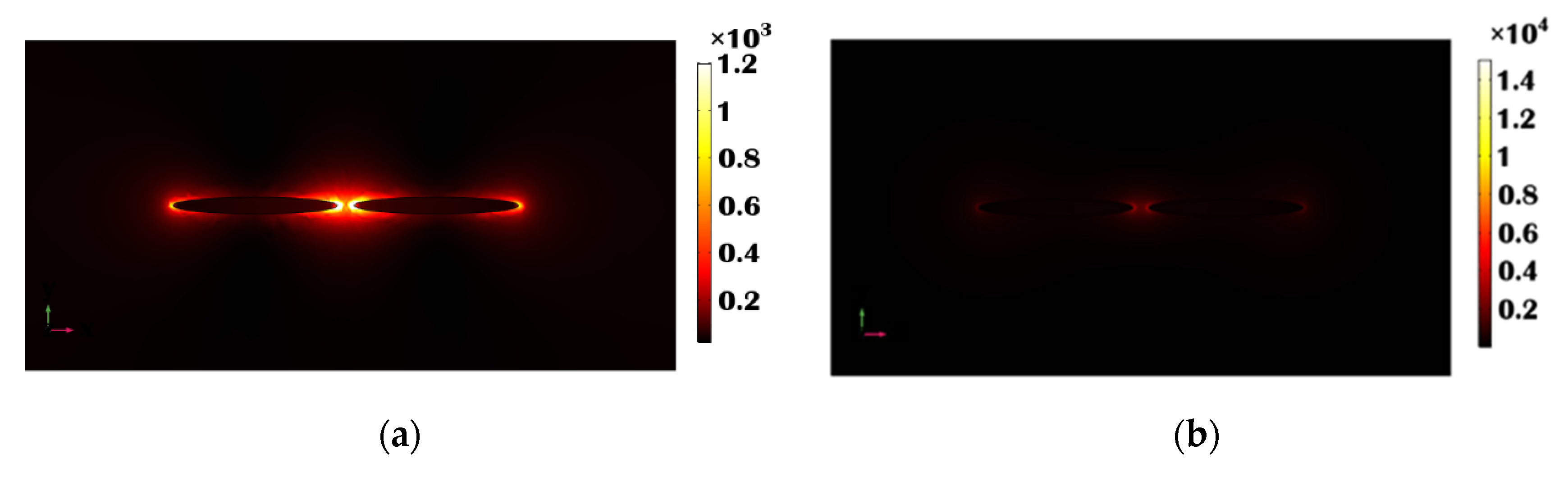
Figure 4.
(a) Electric field distribution along the x plane in the gold elliptical and circular paired structure when a = 100 nm, b = 10, g = 10 nm and h = 10 (b) Electric field distribution along the x plane in the single gold and stacked 10 layers (with LiTaO3 or Al2O3) elliptical paired structure when a = 100 nm, b = 10, g = 10 nm and h1 = h2 = 10 nm. (c) Ey, mode field profile at 940 nm wavelength of a single metallic elliptical nano structure when a = 100 nm, b = 10 nm, and h = 100 nm along the x-z plane (d) Electric field variation at 1000 nm wavelength along the x-z plane for a 10 layered LiTaO3 stacked nano structure when a = 100 nm, b = 10 nm, and h1 = h2 = 10 nm.

Figure 5.
(a) Ex, mode field profile at 940 nm wavelength in the x-y plane of a single metallic elliptical nano structure when a = 100 nm, b = 10 nm, and h = 100 nm, where a slice of the horizontal plane is placed at z = 100 nm. (b) The electric field profile at the 1000 nm wavelength in the x-y plane for a 10 layered LiTaO3 stacked nano structure when a = 100 nm, b = 10 nm, and h1 = h2 = 10 nm, where the slice of the horizontal plane is adjusted at z = 100 nm.

Figure 6.
Sensitivity comparison of 10 layered stacked antenna array (5 gold layers with h1 = 10 nm gold and 5 LiTaO3/Al2O3 layers with a =100 nm, b = 10 nm and h2 (LiTaO3 and Al2O3) = 10 nm) with respect to separation distance.
Figure 6.
Sensitivity comparison of 10 layered stacked antenna array (5 gold layers with h1 = 10 nm gold and 5 LiTaO3/Al2O3 layers with a =100 nm, b = 10 nm and h2 (LiTaO3 and Al2O3) = 10 nm) with respect to separation distance.


Table 1.
Comparision between proposed work with the Tamm sensors.
| S.NO. | The Designed Structure | Sensitivity | Sensing Materials | Ref. |
|---|---|---|---|---|
| 1. | 1D porous silicon photonic crystal fluid sensor based on TP resonance | 5018 nm/RIU | Different fluids | [72] |
| 2. | 1D photonic crystal as a gas sensor based on TP resonance | 273 nm/RIU | Toluene | [73] |
| 3. | Experimental gas sensor based on TP resonance | 70 nm | Organic vapors | [74] |
| 4. | Metallo-dielectric heterostructure configuration based on TP resonance | 970 nm/RIU | Different liquids | [75] |
| 5. | Theoretical gas sensor using photonic crystal cavity based on TP resonance | 450 nm/RIU | Methane gas | [76] |
| 6. | Theoretical elliptical shaped plasmonic nano antenna array | 770 nm/RIU | Water and gases from RI 1.0 to RI 1.7 | This work |
Table 2.
Comparision between the proposed work and the other metallic and hybrid structures.
| S.NO. | Metal | Dielectric | Shape | Sensitivity | FWHM | Ref. |
|---|---|---|---|---|---|---|
| 1. | Silver | GaP | Ring and Heptamer | 550 nm/RIU | 82.4 | [77] |
| 2. | Aluminum | SiO2 | Bow-Tie | 497 nm/RIU | ----- | [78] |
| 3. | Gold | SiO2/SiC | Photonic Crystal | 5.4 nm | ----- | [79] |
| 4. | Silver | Si/SiO2 | Elliptical and MMI waveguide | 550 nm/RIU | 1.947 | [80] |
| 5. | Silver | Si | Ring | 636 nm/RIU | ------ | [81] |
| 6. | Gold | LiTaO3/Al2O3 | Elliptical Stacked | 770 nm/RIU | 76.4 | This Work |
Disclaimer/Publisher’s Note: The statements, opinions and data contained in all publications are solely those of the individual author(s) and contributor(s) and not of MDPI and/or the editor(s). MDPI and/or the editor(s) disclaim responsibility for any injury to people or property resulting from any ideas, methods, instructions or products referred to in the content. |
© 2023 by the authors. Licensee MDPI, Basel, Switzerland. This article is an open access article distributed under the terms and conditions of the Creative Commons Attribution (CC BY) license (https://creativecommons.org/licenses/by/4.0/).
Share and Cite
MDPI and ACS Style
Verma, S.; Rahman, B.M.A. Computational Investigation of Advanced Refractive Index Sensor Using 3-Dimensional Metamaterial Based Nanoantenna Array. Sensors 2023, 23, 1290. https://doi.org/10.3390/s23031290
AMA Style
Verma S, Rahman BMA. Computational Investigation of Advanced Refractive Index Sensor Using 3-Dimensional Metamaterial Based Nanoantenna Array. Sensors. 2023; 23(3):1290. https://doi.org/10.3390/s23031290
Chicago/Turabian StyleVerma, Sneha, and B.M.A. Rahman. 2023. "Computational Investigation of Advanced Refractive Index Sensor Using 3-Dimensional Metamaterial Based Nanoantenna Array" Sensors 23, no. 3: 1290. https://doi.org/10.3390/s23031290
Note that from the first issue of 2016, this journal uses article numbers instead of page numbers. See further details here.