
A Comprehensive Survey on Nanophotonic Neural Networks: Architectures, Training Methods, Optimization, and Activations Functions

 ,
, 

Abstract
:1. Introduction
2. Nature of Light
- (1)
- |𝐸⟩: Quantum condition where, if power is calculated, the result will be E.
- (2)
- |𝑝⟩: Quantum condition where, if momentum is calculated, the result will be p.
- (3)
- |𝑥⟩: Quantum condition where, if position is calculated, the result will be x.
3. Photonic Neuromorphic Processors
- (1)
- Significant reduction of energy consumption in the applications of logical circuits as well as in data transfer.
- (2)
- Exceptionally high operating speeds with no energy consumption other than on the transmitters and the receivers.
- (3)
- Distribution of the computing power in the whole network, with each neuron performing simultaneously small parts of the whole computational activity.
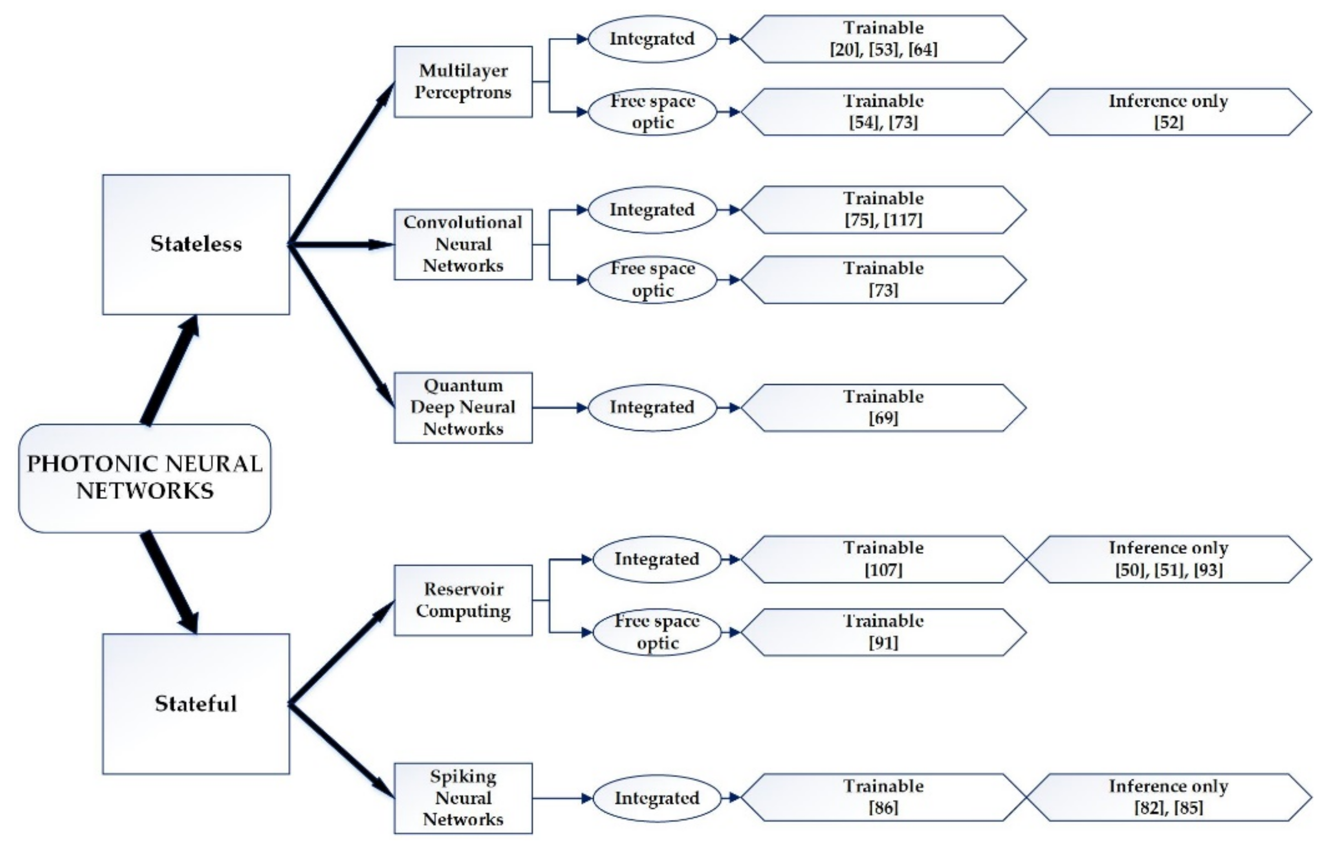
4. Architectures
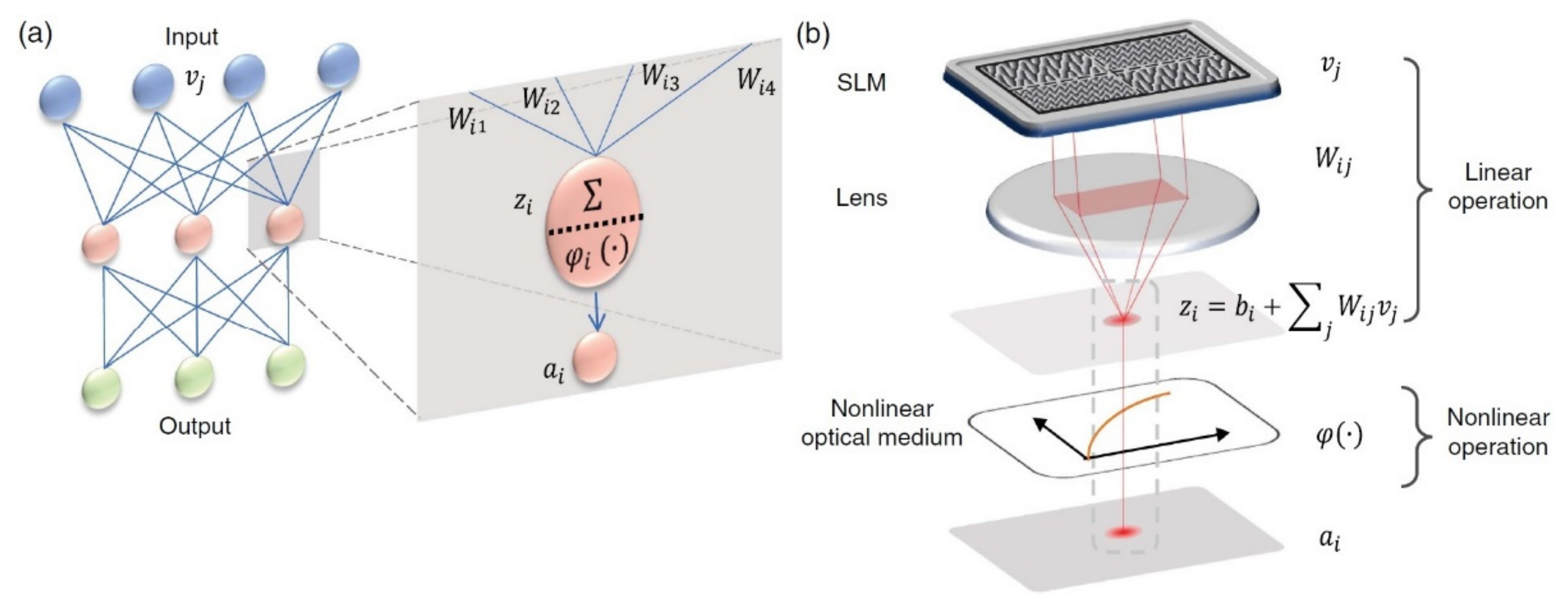
4.1. Perceptron
4.2. Multilayer Perceptrons
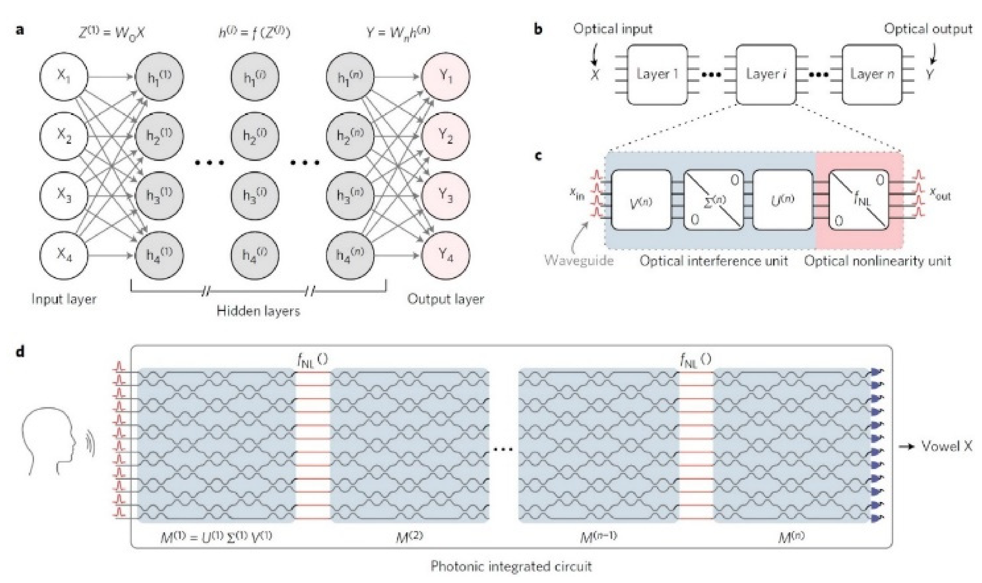
4.3. Deep Photonic Neural Networks
4.4. Convolutional Neural Networks
4.5. Spiking Neural Networks
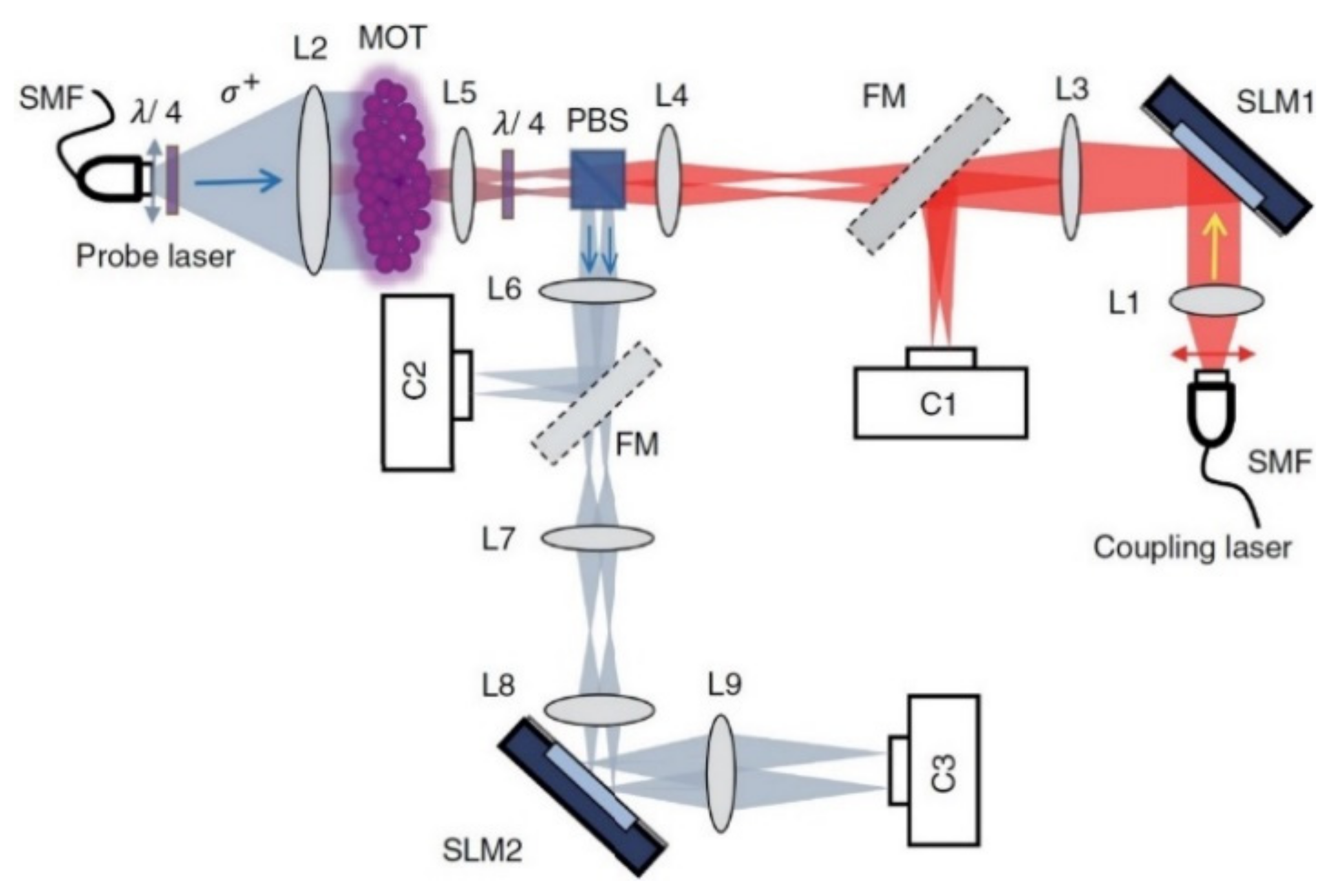
4.6. Reservoir Computing
5. Training Methodologies
5.1. Propagation
5.2. Non-Linearity Inversion
6. Activation Functions
6.1. z–Transform (Complex Non-Linearity)
6.2. Electro-Optical Activation (Complex Non-Linearity)
- (1)
- α: the factor of input power transformation into an electric signal.
- (2)
- R: the response of the photodetector to the optical to electrical unit.
- (3)
- G: the gain of amplification rate.
- (4)
- Vb: the biasing voltage (bias).
- (5)
- Vπ: the required voltage for the π transformation of the phase.
6.3. Sigmoid (Complex Non-Linearity)
6.4. Softmax (Complex Non-Linearity)
6.5. SPM Activation (Non-Linearity)
6.6. zReLU (Non-Linearity)
6.7. Cosine Activation Function (Non-Linearity)
7. Conclusions
- (1)
- Most of the systems do not require energy for the processing of optical signals. As soon as the neural network is trained, the computations on the optical signals are conducted without any additional energy consumption, rendering this particular architecture completely passive.
- (2)
- The optical systems, in contrast to the conventional electronic ones, do not produce heat during their operation and, as a result, they can be enclosed in three-dimensional constructions.
- (3)
- The processing speed in the optical systems is restricted only by the operation frequency of the laser source of light, which reaches 1 THz.
- (4)
- The optical grids enable the multiplication of matrixes with vectors, something which is essential to NNs. The linear transformations (and some non-linear ones) can be performed at the speed of light and detected at a rate of over 100 GHz in photonic networks and, in some cases, with a minimum power consumption.
- (5)
- They are not particularly demanding as far as non-linearities are concerned, since many innate optical non-linearities can be used directly for the application of non-linear operations in PNNs, such as the activation functions.
- (1)
- The dimensions of optical devices are analogous to the light wavelength that they use (400 nm–800 nm).
- (2)
- The mass production of optical devices is limited compared to the electronic ones, since they lack at least 50 years of research and development.
- (3)
- The training of the optical grids is quite difficult because the controlled parameters are active in matrix elements deriving from powerful non-linear functions.
- (4)
- The application of matrix transformations with optical components of mass production (such as fibers and lenses) is a restriction to the spread of ONNs due to the need for stability in the signal phase and to the huge number of neurons, which are required in more complex applications.
Author Contributions
Funding
Institutional Review Board Statement
Informed Consent Statement
Conflicts of Interest
Abbreviations
| ADC | Analog Digital Converter |
| AI | Artificial Intelligence |
| A-MZI | Asynchronous Mach–Zehnder Interferometer |
| AONN | All Optical Neural Network |
| AVM | Adjoint Variable Method |
| CNN | Convolutional Neural Network |
| CPU | Central Processing Unit |
| CW | Continuous Wave |
| DNN | Deep Neural Network |
| DPNN | Deep Photonic Neural Network |
| EIT | Electromagnetically Induced Transparency |
| FDM | Finite Difference Method |
| FM | Flip Mirror |
| GPU | Graphics Processing Unit |
| HL | Hyper-dimensional Learning |
| MAC | Multiply Accumulate Operations |
| MNIST | Modified National Institute of Standards and Technology |
| MOD | Modulator |
| MOT | Magneto-Optical Trap |
| MP | Microprocessor |
| MR | Micro Rings Resonator |
| MUX | Multiplexor |
| MZI | Mach–Zehnder Interferometer |
| MZM | Mach–Zehnder Modulator |
| NN | Neural Network |
| NNN | Nanophotonic Neural Network |
| NSoC | Neuromorphic Systems-on-Chip |
| OCNN | Optical Convolutional Neural Network |
| OIU | Optical Interference Unit |
| OM | Optical Modulator |
| ONN | Optical Neural Network |
| ONU | Optical Non-Linear Unit |
| PCC | Photonic Crystal Cavity |
| PD | Photodetector |
| PNN | Photonic Neural Network |
| PRC | Photonic Reservoir Computing |
| RC | Reservoir Computing |
| RNN | Recurrent neural network |
| ROC | Region Of Convergence |
| SLM | Spatial Light Modulator |
| SMF | Single-Mode Fiber |
| SNN | Spiking Neural Networks |
| SVD | Singular-Value Decomposition |
| TPU | Tensor Processing Unit |
| VOA | Variable Optical Attenuator |
References
- Schrettenbrunnner, M.B. Artificial-Intelligence-Driven Management. IEEE Eng. Manag. Rev. 2020, 48, 15–19. [Google Scholar] [CrossRef]
- Srivastava, S.; Bisht, A.; Narayan, N. Safety and security in smart cities using artificial intelligence—A review. In Proceedings of the 7th International Conference on Cloud Computing, Data Science & Engineering—Confluence, Noida, India, 12–13 January 2017; pp. 130–133. [Google Scholar] [CrossRef]
- Tewari, I.; Pant, M. Artificial Intelligence Reshaping Human Resource Management: A Review. In Proceedings of the IEEE International Conference on Advent Trends in Multidisciplinary Research and Innovation (ICATMRI), Buldhana, India, 30 December 2020; pp. 1–4. [Google Scholar] [CrossRef]
- Quan, X.I.; Sanderson, J. Understanding the Artificial Intelligence Business Ecosystem. IEEE Eng. Manag. Rev. 2018, 46, 22–25. [Google Scholar] [CrossRef]
- Anezakis, V.-D.; Iliadis, L.; Demertzis, K.; Mallinis, G. Hybrid Soft Computing Analytics of Cardiorespiratory Morbidity and Mortality Risk Due to Air Pollution. In Information Systems for Crisis Response and Management in Mediterranean Countries; Dokas, I.M., Saoud, N.B., Dugdale, J., Díaz, P., Eds.; Springer International Publishing: Cham, Switzerland, 2017; Volume 301, pp. 87–105. [Google Scholar] [CrossRef]
- Werbos, P. An overview of neural networks for control. IEEE Control Syst. 1991, 11, 40–41. [Google Scholar] [CrossRef]
- Huang, Y.; Gao, P.; Zhang, Y.; Zhang, J. A Cloud Computing Solution for Big Imagery Data Analytics. In Proceedings of the 2018 International Workshop on Big Geospatial Data and Data Science (BGDDS), Wuhan, China, 22–23 September 2018; pp. 1–4. [Google Scholar] [CrossRef]
- Mahmud, M.S.; Huang, J.Z.; Salloum, S.; Emara, T.Z.; Sadatdiynov, K. A survey of data partitioning and sampling methods to support big data analysis. Big Data Min. Anal. 2020, 3, 85–101. [Google Scholar] [CrossRef]
- Sperduti, A. An overview on supervised neural networks for structures. In Proceedings of the International Conference on Neural Networks (ICNN’97), Houston, TX, USA, 8–10 June 1997; Volume 4, pp. 2550–2554. [Google Scholar] [CrossRef]
- Zhao, C.; Shen, Z.; Zhou, G.Y.; Zhao, C.Z.; Yang, L.; Man, K.L.; Lim, E. Neuromorphic Properties of Memristor towards Artificial Intelligence. In Proceedings of the 2018 International SoC Design Conference (ISOCC), Daegu, Korea, 12–15 November 2018; pp. 172–173. [Google Scholar] [CrossRef]
- Kang, Y. AI Drives Domain Specific Processors. In Proceedings of the 2018 IEEE Asian Solid-State Circuits Conference (A-SSCC), Tainan, Taiwan, 5–7 November 2018; pp. 13–16. [Google Scholar] [CrossRef]
- Chitty-Venkata, K.T.; Somani, A. Impact of Structural Faults on Neural Network Performance. In Proceedings of the 2019 IEEE 30th International Conference on Application-specific Systems, Architectures and Processors (ASAP), New York, NY, USA, 15–17 July 2019; p. 35. [Google Scholar] [CrossRef] [Green Version]
- Li, Z.; Liu, C.; Wang, Y.; Yan, B.; Yang, C.; Yang, J.; Li, H. An overview on memristor crossabr based neuromorphic circuit and architecture. In Proceedings of the 2015 IFIP/IEEE International Conference on Very Large Scale Integration (VLSI-SoC), Daejeon, Korea, 5–7 October 2015; pp. 52–56. [Google Scholar] [CrossRef]
- Blouw, P.; Eliasmith, C. Event-Driven Signal Processing with Neuromorphic Computing Systems. In Proceedings of the ICASSP 2020—2020 IEEE International Conference on Acoustics, Speech and Signal Processing (ICASSP), Barcelona, Spain, 4–8 May 2020; pp. 8534–8538. [Google Scholar] [CrossRef]
- De Lima, T.F.; Peng, H.-T.; Tait, A.N.; Nahmias, M.A.; Miller, H.B.; Shastri, B.J.; Prucnal, P.R. Machine Learning with Neuromorphic Photonics. J. Light. Technol. 2019, 37, 1515–1534. [Google Scholar] [CrossRef]
- Mead, C.; Moore, G.; Moore, B. Neuromorphic engineering: Overview and potential. In Proceedings of the 2005 IEEE International Joint Conference on Neural Networks, Montreal, QC, Canada, 31 July–4 August 2005; Volume 5, p. 3334. [Google Scholar] [CrossRef] [Green Version]
- Zheng, N.; Mazumder, P. Learning in Energy-Efficient Neuromorphic Computing: Algorithm and Architecture Co-Design, 1st ed.; Wiley: Hoboken, NJ, USA, 2019. [Google Scholar] [CrossRef]
- Sui, X.; Wu, Q.; Liu, J.; Chen, Q.; Gu, G. A Review of Optical Neural Networks. IEEE Access 2020, 8, 70773–70783. [Google Scholar] [CrossRef]
- Tsumura, N.; Fujii, Y.; Itoh, K.; Ichioka, Y. Optical method for generalized Hebbian-rule in optical neural network. In Proceedings of the 1993 International Conference on Neural Networks (IJCNN-93-Nagoya, Japan), Nagoya, Japan, 25–29 October 1993; Volume 1, pp. 833–836. [Google Scholar] [CrossRef]
- Abel, S.; Horst, F.; Stark, P.; Dangel, R.; Eltes, F.; Baumgartner, Y.; Fompeyrine, J.; Offrein, B.J. Silicon photonics integration technologies for future computing systems. In Proceedings of the 2019 24th OptoElectronics and Communications Conference (OECC) and 2019 International Conference on Photonics in Switching and Computing (PSC), Fukuoka, Japan, 24 July 2019; pp. 1–3. [Google Scholar] [CrossRef]
- Shastri, B.J.; Tait, A.N.; Nahmias, M.A.; de Lima, T.F.; Peng, H.-T.; Prucnal, P.R. Neuromorphic Photonic Processor Applications. In Proceedings of the 2019 IEEE Photonics Society Summer Topical Meeting Series (SUM), Ft. Lauderdale, FL, USA, 8–10 July 2019; pp. 1–2. [Google Scholar] [CrossRef]
- Yao, J. Photonic integrated circuits for microwave photonics. In Proceedings of the 2017 IEEE Photonics Conference (IPC) Part II, Orlando, FL, USA, 1–5 October 2017; pp. 1–2. [Google Scholar] [CrossRef]
- Zhuang, L.; Xie, Y.; Lowery, A.J. Photonics-enabled innovations in RF engineering. In Proceedings of the 2018 Australian Microwave Symposium (AMS), Brsibane, QLD, Australia, 6–7 February 2018; pp. 7–8. [Google Scholar] [CrossRef]
- Clark, A.S.; Collins, M.J.; Husko, C.; Vo, T.; He, J.; Shahnia, S.; De Rossi, A.; Combrié, S.; Rey, I.H.; Li, J.; et al. Nonlinear Photonics: Quantum State Generation and Manipulation. In Proceedings of the 2014 IEEE Photonics Society Summer Topical Meeting Series, Montreal, QC, Canada, 14–16 July 2014; pp. 140–141. [Google Scholar] [CrossRef]
- Abdelgaber, N.; Nikolopoulos, C. Overview on Quantum Computing and its Applications in Artificial Intelligence. In Proceedings of the 2020 IEEE Third International Conference on Artificial Intelligence and Knowledge Engineering (AIKE), Laguna Hills, CA, USA, 9–13 December 2020; pp. 198–199. [Google Scholar] [CrossRef]
- Prucnal, P.R.; Tait, A.N.; Nahmias, M.A.; de Lima, T.F.; Peng, H.-T.; Shastri, B.J. Multiwavelength Neuromorphic Photonics. In Proceedings of the Conference on Lasers and Electro-Optics, San Jose, CA, USA, 9–14 May 2019; p. JM3M.3. [Google Scholar] [CrossRef]
- Belforte, D. Overview of the laser machining industry. In Proceedings of the CLEO ’99, Conference on Lasers and Electro-Optics (IEEE Cat. No.99CH37013), Baltimore, MD, USA, 28 May 1999; p. 82, In Technical Digest; Summaries of papers presented at the Conference on Lasers and Electro-Optics; Postconference Edition. [Google Scholar] [CrossRef]
- Lancaster, D.G.; Hebert, N.B.; Zhang, W.; Piantedosi, F.; Monro, T.M.; Genest, J. A Multiple-Waveguide Mode-Locked Chip-Laser Architecture. In Proceedings of the 2019 Conference on Lasers and Electro-Optics Europe & European Quantum Electronics Conference (CLEO/Europe-EQEC), Munich, Germany, 23–27 June 2019; p. 1. [Google Scholar] [CrossRef]
- Kleine, K.; Balu, P. High-power diode laser sources for materials processing. In Proceedings of the 2017 IEEE High Power Diode Lasers and Systems Conference (HPD), Coventry, UK, 11–12 October 2017; pp. 3–4. [Google Scholar] [CrossRef]
- Reithmaier, J.P.; Klopf, F.; Krebs, R. Quantum dot lasers for high power and telecommunication applications. In Proceedings of the LEOS 2001 14th Annual Meeting of the IEEE Lasers and Electro-Optics Society (Cat. No.01CH37242), San Diego, CA, USA, 12–13 November 2001; Volume 1, pp. 269–270. [Google Scholar] [CrossRef]
- Renner, D.S.; Jewell, J.; Carlson, N.; Lau, K.; Zory, P. Semiconductor laser workshop—an overview. In Proceedings of the LEOS 93 LEOS-93, San Jose, CA, USA, 15–18 November 1993; p. 724. [Google Scholar] [CrossRef]
- Washio, K. Overview and Recent Topics in Industrial Laser Applications in Japan. In Proceedings of the 2007 Conference on Lasers and Electro-Optics (CLEO), Baltimore, MD, USA, 6–11 May 2007; p. 1. [Google Scholar] [CrossRef]
- Barrera-Singana, C.; Valenzuela, A.; Comech, M.P. Dynamic Control Modelling of a Bipole Converter Station in a Multi-terminal HVDC Grid. In Proceedings of the 2017 International Conference on Information Systems and Computer Science (INCISCOS), Quito, Ecuador, 23–25 November 2017; pp. 146–151. [Google Scholar] [CrossRef]
- Ghannoum, E.; Kieloch, Z. Use of modern technologies and software to deliver efficient design and optimization of 1380 km long bipole III 00 kV HVDC transmission line, Manitoba, Canada. In Proceedings of the PES T&D 2012, Orlando, FL, USA, 7–10 May 2012; pp. 1–6. [Google Scholar] [CrossRef]
- Suriyaarachchi, D.H.R.; Wang, P.; Mohaddes, M.; Zoroofi, S.; Jacobson, D.; Kell, D. Investigation of paralleling Bipole II and the future Bipole III in Nelson River HVDC system. In Proceedings of the 10th IET International Conference on AC and DC Power Transmission (ACDC 2012), Birmingham, UK, 4–6 December 2012; p. 13. [Google Scholar] [CrossRef]
- Bovino, F.A. On chip intrasystem quantum entangled states generator. In Proceedings of the 2017 Conference on Lasers and Electro-Optics Europe & European Quantum Electronics Conference (CLEO/Europe-EQEC), Munich, Germany, 20–24 June 2017; p. 1. [Google Scholar] [CrossRef]
- Lund, A.P.; Ralph, T.C. Efficient coherent state quantum computing by adaptive measurements. In Proceedings of the 2006 Conference on Lasers and Electro-Optics and 2006 Quantum Electronics and Laser Science Conference, Long Beach, CA, USA, 21–26 May 2006; pp. 1–2. [Google Scholar] [CrossRef]
- Knight, P.L. Quantum communication and quantum computing. In Proceedings of the Quantum Electronics and Laser Science Conference, Baltimore, MD, USA, 23–26 May 1999; p. 32, Technical Digest; Summaries of Papers Presented at the Quantum Electronics and Laser Science Conference. [Google Scholar] [CrossRef]
- Ferrari, D.; Cacciapuoti, A.S.; Amoretti, M.; Caleffi, M. Compiler Design for Distributed Quantum Computing. IEEE Trans. Quantum Eng. 2021, 2, 1–20. [Google Scholar] [CrossRef]
- Silverstone, J.W.; Thompson, M.; Rarity, J.G.; Rosenfeld, L.M.; Sulway, D.A.; Sayers, B.D.J.; Biele, J.; Sinclair, G.F.; Sahin, D.; Kling, L.; et al. Silicon Quantum Photonics in the Short-Wave Infrared: A New Platform for Big Quantum Optics. In Proceedings of the 2019 Conference on Lasers and Electro-Optics Europe & European Quantum Electronics Conference (CLEO/Europe-EQEC), Munich, Germany, 23–27 June 2019; p. 1. [Google Scholar] [CrossRef]
- Arun, G.; Mishra, V. A review on quantum computing and communication. In Proceedings of the 2014 2nd International Conference on Emerging Technology Trends in Electronics, Communication and Networking, Surat, India, 17–18 December 2014; pp. 1–5. [Google Scholar] [CrossRef]
- Ding, Y.; Llewellyn, D.; Faruque, I.I.; Bacco, D.; Rottwitt, K.; Thompson, M.G.; Wang, J.; Oxenlowe, L.K. Quantum Entanglement and Teleportation Based on Silicon Photonics. In Proceedings of the 2020 22nd International Conference on Transparent Optical Networks (ICTON), Bari, Italy, 19–23 July 2020; pp. 1–4. [Google Scholar] [CrossRef]
- De Adelhart Toorop, R.; Bazzocchi, F.; Merlo, L.; Paris, A. Constraining flavour symmetries at the EW scale I: The A 4 Higgs potential. J. High Energy Phys. 2011, 2011, 35. [Google Scholar] [CrossRef] [Green Version]
- Khan, M.U.; Xing, Y.; Ye, Y.; Bogaerts, W. Photonic Integrated Circuit Design in a Foundry+Fabless Ecosystem. IEEE J. Sel. Top. Quantum Electron. 2019, 25, 1–14. [Google Scholar] [CrossRef]
- Parhi, K.K.; Unnikrishnan, N.K. Brain-Inspired Computing: Models and Architectures. IEEE Open J. Circuits Syst. 2020, 1, 185–204. [Google Scholar] [CrossRef]
- El-Kady, I.; Taha, M.M.R. Nano Photonic Sensors for Microdamage Detection: An Exploratory Simulation. In Proceedings of the 2005 IEEE International Conference on Systems, Man and Cybernetics, Waikoloa, HI, USA, 10–12 October 2005; Volume 2, pp. 1961–1966. [Google Scholar] [CrossRef]
- Noda, S.; Asano, T.; Imada, M. Novel nanostructures for light: Photonic crystals. In Proceedings of the 2003 Third IEEE Conference on Nanotechnology, IEEE-NANO 2003, San Francisco, CA, USA, 12–14 August 2003; Volume 2, pp. 277–278. [Google Scholar] [CrossRef]
- Vuckovic, J.; Yoshie, T.; Loncar, M.; Mabuchi, H.; Scherer, A. Nano-scale optical and quantum optical devices based on photonic crystals. In Proceedings of the 2nd IEEE Conference on Nanotechnology, Washington, DC, USA, 26–28 August 2002; pp. 319–321. [Google Scholar] [CrossRef] [Green Version]
- De Marinis, L.; Cococcioni, M.; Castoldi, P.; Andriolli, N. Photonic Neural Networks: A Survey. IEEE Access 2019, 7, 175827–175841. [Google Scholar] [CrossRef]
- Vandoorne, K.; Mechet, P.; Van Vaerenbergh, T.; Fiers, M.; Morthier, G.; Verstraeten, D.; Schrauwen, B.; Dambre, J.; Bienstman, P. Experimental demonstration of reservoir computing on a silicon photonics chip. Nat. Commun. 2014, 5, 3541. [Google Scholar] [CrossRef] [Green Version]
- Coarer, F.D.-L.; Sciamanna, M.; Katumba, A.; Freiberger, M.; Dambre, J.; Bienstman, P.; Rontani, D. All-Optical Reservoir Computing on a Photonic Chip Using Silicon-Based Ring Resonators. IEEE J. Sel. Top. Quantum Electron. 2018, 24, 1–8. [Google Scholar] [CrossRef] [Green Version]
- Lin, X.; Rivenson, Y.; Yardimci, N.T.; Veli, M.; Luo, Y.; Jarrahi, M.; Ozcan, A. All-optical machine learning using diffractive deep neural networks. Science 2018, 361, 1004–1008. [Google Scholar] [CrossRef] [Green Version]
- Shi, B.; Calabretta, N.; Stabile, R. Image Classification with a 3-Layer SOA-Based Photonic Integrated Neural Network. In Proceedings of the 2019 24th OptoElectronics and Communications Conference (OECC) and 2019 International Conference on Photonics in Switching and Computing (PSC), Fukuoka, Japan, 7 July 2019; pp. 1–3. [Google Scholar] [CrossRef]
- Zuo, Y.; Li, B.; Zhao, Y.; Jiang, Y.; Chen, Y.-C.; Chen, P.; Jo, G.-B.; Liu, J.; Du, S. All-optical neural network with nonlinear activation functions. Optica 2019, 6, 1132. [Google Scholar] [CrossRef]
- Harris, S.E. Electromagnetically Induced Transparency. Phys. Today 1997, 50, 36–42. [Google Scholar] [CrossRef]
- Raab, E.L.; Prentiss, M.; Cable, A.; Chu, S.; Pritchard, D.E. Trapping of Neutral Sodium Atoms with Radiation Pressure. Phys. Rev. Lett. 1987, 59, 2631–2634. [Google Scholar] [CrossRef] [Green Version]
- Grabowski, A.; Pfau, T. A lattice of magneto-optical and magnetic traps for cold atoms. In Proceedings of the 2003 European Quantum Electronics Conference. EQEC 2003 (IEEE Cat No.03TH8665), Munich, Germany, 22–27 June 2003; p. 274. [Google Scholar] [CrossRef] [Green Version]
- Grossman, J.M.; Aubin, S.; Gomez, E.; Orozco, L.; Pearson, M.; Sprouse, G.; True, M. New apparatus for magneto-optical trapping of francium. In Proceedings of the Quantum Electronics and Laser Science Conference (IEEE Cat. No.01CH37172), Baltimore, MD, USA, 6–11 May 2001; p. 220, Technical Digest; Summaries of papers presented at the Quantum Electronics and Laser Science Conference; Postconference Technical Digest. [Google Scholar] [CrossRef]
- The Ising Model. Available online: http://stanford.edu/~jeffjar/statmech2/intro4.html (accessed on 8 March 2020).
- Singh, J.; Singh, M. Evolution in Quantum Computing. In Proceedings of the 2016 International Conference System Modeling & Advancement in Research Trends (SMART), Moradabad, India, 25–27 November 2016; pp. 267–270. [Google Scholar] [CrossRef]
- Yatsui, T.; Ohtsu, M. Development of nano-photonic devices and their integration by optical near field. In Proceedings of the IEEE/LEOS International Conference on Optical MEMs, Lugano, Switzerland, 20–23 August 2002; pp. 199–200. [Google Scholar] [CrossRef]
- Olyaee, S.; Ebrahimpur, R.; Esfandeh, S. A hybrid genetic algorithm-neural network for modeling of periodic nonlinearity in three-longitudinal-mode laser heterodyne interferometer. In Proceedings of the 2013 21st Iranian Conference on Electrical Engineering (ICEE), Mashhad, Iran, 14–16 May 2013; pp. 1–5. [Google Scholar] [CrossRef]
- Ren, Z.; Pope, S.B. The geometry of reaction trajectories and attracting manifolds in composition space. Combust. Theory Model. 2006, 10, 361–388. [Google Scholar] [CrossRef]
- Shen, Y.; Harris, N.C.; Skirlo, S.; Prabhu, M.; Baehr-Jones, T.; Hochberg, M.; Sun, X.; Zhao, S.; LaRochelle, H.; Englund, D.; et al. Deep learning with coherent nanophotonic circuits. Nat. Photon. 2017, 11, 441–446. [Google Scholar] [CrossRef]
- Howland, P.; Park, H. Generalizing discriminant analysis using the generalized singular value decomposition. IEEE Trans. Pattern Anal. Mach. Intell. 2004, 26, 995–1006. [Google Scholar] [CrossRef]
- Zhang, Q.; Qin, Y. Adaptive Singular Value Decomposition and its Application to the Feature Extraction of Planetary Gearboxes. In Proceedings of the 2017 International Conference on Sensing, Diagnostics, Prognostics, and Control (SDPC), Shanghai, China, 16–18 August 2017; pp. 488–492. [Google Scholar] [CrossRef]
- Zhou, B.; Liu, Z. Method of Multi-resolution and Effective Singular Value Decomposition in Under-determined Blind Source Separation and Its Application to the Fault Diagnosis of Roller Bearing. In Proceedings of the 2015 11th International Conference on Computational Intelligence and Security (CIS), Shenzhen, China, 19–20 December 2015; pp. 462–465. [Google Scholar] [CrossRef]
- Shen, Y.; Bai, Y. Statistical Computing with Integrated Photonics System. In Proceedings of the 2019 24th OptoElectronics and Communications Conference (OECC) and 2019 International Conference on Photonics in Switching and Computing (PSC), Fukuoka, Japan, 16–17 July 2019; p. 1. [Google Scholar] [CrossRef]
- Leelar, B.S.; Shivaleela, E.S.; Srinivas, T. Learning with Deep Photonic Neural Networks. In Proceedings of the 2017 IEEE Workshop on Recent Advances in Photonics (WRAP), Hyderabad, India, 18–19 December 2017; pp. 1–7. [Google Scholar] [CrossRef]
- Li, Z.; Liu, F.; Yang, W.; Peng, S.; Zhou, J. A Survey of Convolutional Neural Networks: Analysis, Applications, and Prospects. IEEE Trans. Neural Netw. Learn. Syst. 2021, 1–21. [Google Scholar] [CrossRef]
- Saha, S. A Comprehensive Guide to Convolutional Neural Networks—The ELI5 Way. 2018. Available online: https://towardsdatascience.com/a-comprehensive-guide-to-convolutional-neural-networks-the-eli5-way-3bd2b1164a53 (accessed on 11 March 2020).
- Hamerly, R.; Sludds, A.; Bernstein, L.; Prabhu, M.; Roques-Carmes, C.; Carolan, J.; Yamamoto, Y.; Soljacic, M.; Englund, D. Towards Large-Scale Photonic Neural-Network Accelerators. In Proceedings of the 2019 IEEE International Electron Devices Meeting (IEDM), San Francisco, CA, USA, 7–11 December 2019; pp. 22.8.1–22.8.4. [Google Scholar] [CrossRef]
- Hamerly, R.; Bernstein, L.; Sludds, A.; Soljačić, M.; Englund, D. Large-Scale Optical Neural Networks Based on Photoelectric Multiplication. Phys. Rev. X 2019, 9, 021032. [Google Scholar] [CrossRef] [Green Version]
- Mrozek, T. Simultaneous Monitoring of Chromatic Dispersion and Optical Signal to Noise Ratio in Optical Network Using Asynchronous Delay Tap Sampling and Convolutional Neural Network (Deep Learning). In Proceedings of the 2018 20th International Conference on Transparent Optical Networks (ICTON), Bucharest, Romania, 1–5 July 2018; pp. 1–4. [Google Scholar] [CrossRef]
- Bagherian, H.; Skirlo, S.; Shen, Y.; Meng, H.; Ceperic, V.; Soljacic, M. On-Chip Optical Convolutional Neural Networks. arXiv 2018, arXiv:1808.03303. [Google Scholar]
- Li, S.-L.; Li, J.-P. Research on Learning Algorithm of Spiking Neural Network. In Proceedings of the 2019 16th International Computer Conference on Wavelet Active Media Technology and Information Processing, Chengdu, China, 13–14 December 2019; pp. 45–48. [Google Scholar] [CrossRef]
- Stewart, T.C.; Eliasmith, C. Large-Scale Synthesis of Functional Spiking Neural Circuits. Proc. IEEE 2014, 102, 881–898. [Google Scholar] [CrossRef]
- Demertzis, K.; Iliadis, L. A Hybrid Network Anomaly and Intrusion Detection Approach Based on Evolving Spiking Neural Network Classification. In E-Democracy, Security, Privacy and Trust in a Digital World; Sideridis, A.B., Kardasiadou, Z., Yialouris, C.P., Zorkadis, V., Eds.; Springer International Publishing: Cham, Switzerland, 2014; Volume 441, pp. 11–23. [Google Scholar] [CrossRef]
- Demertzis, K.; Iliadis, L.; Bougoudis, I. Gryphon: A semi-supervised anomaly detection system based on one-class evolving spiking neural network. Neural Comput. Appl. 2019, 32, 4303–4314. [Google Scholar] [CrossRef]
- Demertzis, K.; Iliadis, L.; Spartalis, S. A Spiking One-Class Anomaly Detection Framework for Cyber-Security on Industrial Control Systems. In Engineering Applications of Neural Networks; Boracchi, G., Iliadis, L., Jayne, C., Likas, A., Eds.; Springer International Publishing: Cham, Switzerland, 2017; Volume 744, pp. 122–134. [Google Scholar] [CrossRef]
- Demertzis, K.; Iliadis, L.; Anezakis, V.-D. A deep spiking machine-hearing system for the case of invasive fish species. In Proceedings of the 2017 IEEE International Conference on INnovations in Intelligent SysTems and Applications (INISTA), Gdynia, Poland, 3–5 July 2017; pp. 23–28. [Google Scholar] [CrossRef]
- Shastri, B.J.; Nahmias, M.A.; Tait, A.N.; Rodriguez, A.W.; Wu, B.; Prucnal, P.R. Spike processing with a graphene excitable laser. Sci. Rep. 2016, 6, srep19126. [Google Scholar] [CrossRef] [Green Version]
- Lobo, J.L.; Del Ser, J.; Bifet, A.; Kasabov, N. Spiking Neural Networks and online learning: An overview and perspectives. Neural Networks 2019, 121, 88–100. [Google Scholar] [CrossRef]
- Van Vaerenbergh, T.; Fiers, M.; Bienstman, P.; Dambre, J. Towards integrated optical spiking neural networks: Delaying spikes on chip. In Proceedings of the 2013 Sixth “Rio De La Plata” Workshop on Laser Dynamics and Nonlinear Photonics, Montevideo, Uruguay, 9–12 December 2013; pp. 1–2. [Google Scholar] [CrossRef]
- Yang, Y.; Deng, Y.; Xiong, X.; Shi, B.; Ge, L.; Wu, J. Neuron-Like Optical Spiking Generation Based on Silicon Microcavity. In Proceedings of the 2020 IEEE 20th International Conference on Communication Technology (ICCT), Nanning, China, 28–31 October 2020; pp. 970–974. [Google Scholar] [CrossRef]
- Nahmias, M.A.; Peng, H.-T.; De Lima, T.F.; Huang, C.; Tait, A.N.; Shastri, B.J.; Prucnal, P.R. A TeraMAC Neuromorphic Photonic Processor. In Proceedings of the 2018 IEEE Photonics Conference (IPC), Reston, VA, USA, 30 September–4 October 2018; pp. 1–2. [Google Scholar] [CrossRef]
- Spoorthi, H.R.; Narendra, C.P.; Mohan, U.C. Low Power Datapath Architecture for Multiply—Accumulate (MAC) Unit. In Proceedings of the 2019 4th International Conference on Recent Trends on Electronics, Information, Communication & Technology (RTEICT), Bangalore, India, 17–18 May 2019; pp. 391–395. [Google Scholar] [CrossRef]
- Stelling, P.F.; Oklobdzija, V.G. Implementing multiply-accumulate operation in multiplication time. In Proceedings of the 13th IEEE Sympsoium on Computer Arithmetic, Asilomar, CA, USA, 6–9 July 1997; pp. 99–106. [Google Scholar] [CrossRef]
- Bala, A.; Ismail, I.; Ibrahim, R.; Sait, S.M. Applications of Metaheuristics in Reservoir Computing Techniques: A Review. IEEE Access 2018, 6, 58012–58029. [Google Scholar] [CrossRef]
- Demertzis, K.; Iliadis, L.; Pimenidis, E. Geo-AI to aid disaster response by memory-augmented deep reservoir computing. Integr. Comput. Eng. 2021, 28, 383–398. [Google Scholar] [CrossRef]
- Li, S.; Pachnicke, S. Photonic Reservoir Computing in Optical Transmission Systems. In Proceedings of the 2020 IEEE Photonics Society Summer Topicals Meeting Series (SUM), Cabo San Lucas, Mexico, 13–15 July 2020; pp. 1–2. [Google Scholar] [CrossRef]
- Vandoorne, K.; Fiers, M.; Verstraeten, D.; Schrauwen, B.; Dambre, J.; Bienstman, P. Photonic reservoir computing: A new approach to optical information processing. In Proceedings of the 2010 12th International Conference on Transparent Optical Networks, Munich, Germany, 29 June–1 July 2010; pp. 1–4. [Google Scholar] [CrossRef] [Green Version]
- Laporte, F.; Katumba, A.; Dambre, J.; Bienstman, P. Numerical demonstration of neuromorphic computing with photonic crystal cavities. Opt. Express 2018, 26, 7955. [Google Scholar] [CrossRef]
- Peng, B.; Özdemir, K.; Chen, W.; Nori, F.; Yang, L. What is and what is not electromagnetically induced transparency in whispering-gallery microcavities. Nat. Commun. 2014, 5, 5082. [Google Scholar] [CrossRef] [PubMed]
- Shi, W.; Lin, J.; Sepehrian, H.; Zhalehpour, S.; Guo, M.; Zhang, Z.; Rusch, L.A. Silicon Photonics for Coherent Optical Transmissions (Invited paper). In Proceedings of the 2019 Photonics North (PN), Quebec City, QC, Canada, 21–23 May 2019; p. 1. [Google Scholar] [CrossRef]
- Hughes, T.W.; Minkov, M.; Shi, Y.; Fan, S. Training of photonic neural networks through in situ backpropagation and gradient measurement. Optica 2018, 5, 864. [Google Scholar] [CrossRef]
- Garrett, A.J.M.; Jaynes, E.T. Review: Probability Theory: The Logic of Science. Law Probab. Risk 2004, 3, 243–246. [Google Scholar] [CrossRef] [Green Version]
- Ohnishi, R.; Wu, D.; Yamaguchi, T.; Ohnuki, S. Numerical Accuracy of Finite-Difference Methods. In Proceedings of the 2018 International Symposium on Antennas and Propagation (ISAP), Busan, Korea, 23–26 October 2018; pp. 1–2. [Google Scholar]
- Serteller, N.F.O. Electromagnetic Wave Propagation Equations in 2D by Finite Difference Method: Mathematical Case. In Proceedings of the 2019 3rd International Symposium on Multidisciplinary Studies and Innovative Technologies (ISMSIT), Ankara, Turkey, 11–13 October 2019; pp. 1–5. [Google Scholar] [CrossRef]
- Xu, L.; Zhengyu, W.; Guohua, L.; Yinlu, C. Numerical simulation of elastic wave based on the staggered grid finite difference method. In Proceedings of the 2011 International Conference on Consumer Electronics, Communications and Networks (CECNet), Xianning, China, 11–13 April 2011; pp. 3283–3286. [Google Scholar] [CrossRef]
- Hussain, M.A.; Tsai, T.-H. An Efficient and Fast Softmax Hardware Architecture (EFSHA) for Deep Neural Networks. In Proceedings of the 2021 IEEE 3rd International Conference on Artificial Intelligence Circuits and Systems (AICAS), Washington, DC, USA, 6–9 June 2021; pp. 1–4. [Google Scholar] [CrossRef]
- Rao, Q.; Yu, B.; He, K.; Feng, B. Regularization and Iterative Initialization of Softmax for Fast Training of Convolutional Neural Networks. In Proceedings of the 2019 International Joint Conference on Neural Networks (IJCNN), Budapest, Hungary, 14–19 July 2019; pp. 1–8. [Google Scholar] [CrossRef]
- Igarashi, H.; Watanabe, K. Complex Adjoint Variable Method for Finite-Element Analysis of Eddy Current Problems. IEEE Trans. Magn. 2010, 46, 2739–2742. [Google Scholar] [CrossRef] [Green Version]
- Zhang, Y.; Negm, M.H.; Bakr, M.H. An Adjoint Variable Method for Wideband Second-Order Sensitivity Analysis Through FDTD. IEEE Trans. Antennas Propag. 2015, 64, 675–686. [Google Scholar] [CrossRef]
- Walker, E.P.; Feng, W.; Zhang, Y.; Zhang, H.; McCormick, F.B.; Esener, S. 3-D parallel readout in a 3-D multilayer optical data storage system. In Proceedings of the International Symposium on Optical Memory and Optical Data Storage Topical Meeting, Waikoloa, HI, USA, 7–11 July 2002; pp. 147–149. [Google Scholar] [CrossRef]
- Arai, Y. Vertical integration of radiation sensors and readout electronics. In Proceedings of the Melecon 2010—2010 15th IEEE Mediterranean Electrotechnical Conference, Valletta, Malta, 26–28 April 2010; pp. 1062–1067. [Google Scholar] [CrossRef]
- Freiberger, M.; Katumba, A.; Bienstman, P.; Dambre, J. Training Passive Photonic Reservoirs with Integrated Optical Readout. IEEE Trans. Neural Netw. Learn. Syst. 2018, 30, 1943–1953. [Google Scholar] [CrossRef]
- Kim, I.; Vassilieva, O.; Akasaka, Y.; Palacharla, P.; Ikeuchi, T. Enhanced Spectral Inversion for Fiber Nonlinearity Mitigation. IEEE Photon-Technol. Lett. 2018, 30, 2040–2043. [Google Scholar] [CrossRef]
- Umeki, T.; Kazama, T.; Ono, H.; Miyamoto, Y.; Takenouchi, H. Spectrally efficient optical phase conjugation based on complementary spectral inversion for nonlinearity mitigation. In Proceedings of the 2015 European Conference on Optical Communication (ECOC), Valencia, Spain, 27 September–1 October 2015; pp. 1–3. [Google Scholar] [CrossRef]
- Williamson, I.A.D.; Hughes, T.W.; Minkov, M.; Bartlett, B.; Pai, S.; Fan, S. Reprogrammable Electro-Optic Nonlinear Activation Functions for Optical Neural Networks. IEEE J. Sel. Top. Quantum Electron. 2019, 26, 1–12. [Google Scholar] [CrossRef] [Green Version]
- Li, J.; Dai, J. Z-Transform Implementations of the CFS-PML. IEEE Antennas Wirel. Propag. Lett. 2006, 5, 410–413. [Google Scholar] [CrossRef]
- Watanabe, T. An optimized SAW chirp -Z Transform for OFDM systems. In Proceedings of the 2009 IEEE International Frequency Control Symposium Joint with the 22nd European Frequency and Time forum, Besancon, France, 20–24 April 2009; pp. 416–419. [Google Scholar] [CrossRef]
- Zhang, Q.; Zong, Z. A New Method for Bistatic SAR Imaging Based on Chirp-Z Transform. In Proceedings of the 2014 Seventh International Symposium on Computational Intelligence and Design, Hangzhou, China, 13–14 December 2014; pp. 236–239. [Google Scholar] [CrossRef]
- Chung, W.; Johnson, C.R. Characterization of the regions of convergence of CMA adapted blind fractionally spaced equalizer. In Proceedings of the Conference Record of Thirty-Second Asilomar Conference on Signals, Systems and Computers (Cat. No.98CH36284), Pacific Grove, CA, USA, 1–4 November 1998; Volume 1, pp. 493–497. [Google Scholar] [CrossRef]
- Fan, F.; Hu, J.; Zhu, W.; Gu, Y.; Zhao, M. A multi-frequency optoelectronic oscillator based on a dual-output Mach-Zender modulator and stimulated brillouin scattering. In Proceedings of the 2017 IEEE Photonics Conference (IPC), Orlando, FL, USA, 1–5 October 2017; pp. 667–668. [Google Scholar] [CrossRef]
- Magazzu, G.; Ciarpi, G.; Saponara, S. Design of a radiation-tolerant high-speed driver for Mach Zender Modulators in High Energy Physics. In Proceedings of the 2018 IEEE International Symposium on Circuits and Systems (ISCAS), Florence, Italy, 27–30 May 2018; pp. 1–5. [Google Scholar] [CrossRef]
- Passalis, N.; Mourgias-Alexandris, G.; Tsakyridis, A.; Pleros, N.; Tefas, A. Training Deep Photonic Convolutional Neural Networks with Sinusoidal Activations. IEEE Trans. Emerg. Top. Comput. Intell. 2019, 5, 384–393. [Google Scholar] [CrossRef]
- Datta, S.; Antonio, R.A.G.; Ison, A.R.S.; Rabaey, J.M. A Programmable Hyper-Dimensional Processor Architecture for Human-Centric IoT. IEEE J. Emerg. Sel. Top. Circuits Syst. 2019, 9, 439–452. [Google Scholar] [CrossRef]
- Kanerva, P. Hyperdimensional Computing: An Introduction to Computing in Distributed Representation with High-Dimensional Random Vectors. Cogn. Comput. 2009, 1, 139–159. [Google Scholar] [CrossRef]


Publisher’s Note: MDPI stays neutral with regard to jurisdictional claims in published maps and institutional affiliations. |
© 2022 by the authors. Licensee MDPI, Basel, Switzerland. This article is an open access article distributed under the terms and conditions of the Creative Commons Attribution (CC BY) license (https://creativecommons.org/licenses/by/4.0/).
Share and Cite
Demertzis, K.; Papadopoulos, G.D.; Iliadis, L.; Magafas, L. A Comprehensive Survey on Nanophotonic Neural Networks: Architectures, Training Methods, Optimization, and Activations Functions. Sensors 2022, 22, 720. https://doi.org/10.3390/s22030720
Demertzis K, Papadopoulos GD, Iliadis L, Magafas L. A Comprehensive Survey on Nanophotonic Neural Networks: Architectures, Training Methods, Optimization, and Activations Functions. Sensors. 2022; 22(3):720. https://doi.org/10.3390/s22030720
Chicago/Turabian StyleDemertzis, Konstantinos, Georgios D. Papadopoulos, Lazaros Iliadis, and Lykourgos Magafas. 2022. "A Comprehensive Survey on Nanophotonic Neural Networks: Architectures, Training Methods, Optimization, and Activations Functions" Sensors 22, no. 3: 720. https://doi.org/10.3390/s22030720