1. Introduction
Acoustic emission (AE) is a nondestructive technique used in a structural health monitoring (SHM) technique and material characterization. The technique relies on receivers to detect elastic waves generated by a change in the structural integrity [
1]. The elastic waves involved are characterized by amplitudes in the nanometer range [
2], therefore, monitoring structures by AE requires sensors with a suitable sensitivity and signal-to-noise ratio [
3].
Up to now, the detection of acoustic emissions has usually been performed by piezoelectric sensors [
4] because of their important feedback from applications in the field of nondestructive testing, either as transmitter or receiver. Their characteristics intrinsically give them a limited frequency bandwidth and an impedance mismatch with respect to the wave propagation medium of the waves (typically, 35 MRayls for piezoelectric against 17 MRayls for aluminum and about 2 MRayls for the coupling material). However, these problems are partly solved by the addition of a backing material improving the sensitivity and enlarging the bandwidth [
5,
6] and front-side matching layers to adapt the acoustic impedance of the tested materials.
Capacitive micromachined ultrasonic transducers (CMUTs) can be an alternative to piezoelectric sensors [
7,
8], particularly because they benefit from the advantages of microelectronics: ease of mass production, miniaturization, flexibility and therefore, integration into complex devices and different topologies. Acting like microphones, CMUTs are capacitive membranes that vibrate under dynamic excitations (as acoustic waves). The mechanical vibrations induce capacitance variations and thus measurable electrical currents. CMUTs are generally characterized by a large bandwidth and low impedance making them well-adapted to acoustic emission applications. However, the low signal-to-noise ratio and sensitivity are clearly the weak points of CMUTs that are tackled in several publications.
About CMUT design, theoretical studies have shown the influence of electrode size on their efficiency. Indeed, the size of the electrodes acts on the parasitic capacitance, hence on the sensitivity and bandwidth of CMUT [
9]. Membrane configuration can also be an important study parameter to increase the performance of CMUT. Manufactured by a wafer bonding process, Huang et al. [
10] compared three different membrane configurations (rectangular, tent and square) at a bias voltage of 20 V. The two configurations tent and rectangular were found to have higher sensitivity than the square one (65% and 44%, respectively) in received mode.
Concerning the configuration of electrical connections, Cheng et al. [
11] presented a solution of electrical interconnections reducing the parasitic capacitance from 2.75 pF to 1.5 pF, thus improving the efficiency of CMUT. To reduce noise, Gurun et al. [
12] removed the wire bonding and the bonding pad between the CMUT and the amplifier. Indeed, this is because the wiring and the bonding pad add parasitic capacitance, which increases noise and decreases the sensitivity of the CMUT.
Regarding the conversion of mechanical vibrations into an electrical signal, Wright [
13] optimized the sensitivity of a MEMS sensor by designing a new transimpedance amplifier (LMV 972). This amplifier increased the signal-to-noise ratio from 8.4 [
V/
V] to 41.2 [
V/
V] for the MEMS sensor, which remained low compared to the signal-to-noise ratio of piezoelectric sensors (475 [
V/
V]).
Especially for AE applications, Ozevin et al. [
14] developed a narrow-band CMUT manufactured by MUMPs. The proper functioning of the CMUT required a vacuum package for better sensitivity. Ozevin et al. [
15] improved their previous CMUT by increasing the active area of the CMUT (from 2.51 mm
2 to 6.97 mm
2) and thus its sensitivity allowing the sensor to operate at atmospheric pressure. Using six independent transducers, Ozevin et al. [
16] developed capacitive MEMS covering a frequency range 100 kHz to 500 kHz. For the 100-unit cells, the maximum detected amplitude to the response of the pencil lead breaking on the ceramic package is 0.05 volt, which remains a low-level sensitivity.
Saboonchi and Ozevin [
17] have compared MEMS AE transducers manufactured by an electroplating technique with piezoelectric transducers having a similar frequency range (50–200 kHz). The results of their experiment showed the good sensitivity of capacitive MEMS AE transducers with a signal-to-noise ratio close to piezoelectric sensors (34.42 dB for MEMS-S1 vs. 42.65 dB for piezoelectric R6) and better than piezoelectric at the central frequency (58.76 dB for MEMS-S1 vs. 54.66 dB for piezoelectric R6). However, the transducers are sensitive to a single wave direction, which can be disadvantageous in case of damage inside the materials.
In a previous article [
7], we presented the application potential of a CMUT-based AE sensor realized by the design of a first version of the sensor (called CMUT-V1 in the following) manufactured using the polyMUMPS surface micromachining process. This previous work focused more particularly on two positive aspects: the multifrequency aspect involving different individual membranes and the bandwidth aspect including the intrinsic capabilities of an array of 9 identical membranes.
This paper proposes to study how to improve the signal-to-noise ratio and especially the sensitivity of these sensors by various potential means such as design, packaging, signal processing and structure-sensor coupling. In
Section 2, a second version of the sensor, fabricated with the same manufacturing MUMPS process and named CMUT-R100 in the following, is presented including practical modifications in design, electrical connections and packaging. Experimental tests show a significant increase in sensitivity and in turn, in the signal-to-noise ratio. Therefore, a classical frequency filtering method is applied to show the interest of designing hardware solutions that achieve this filtering. In
Section 3, the overall sensor sensitivity is divided into an acoustic-mechanical part and a mechanical-electrical one. The acoustic-mechanical contribution mainly determined by the monitored structure-sensor coupling interface is studied according to theoretical and experimental reflection elements. The mechanical-electrical contribution defined by the relation between the mechanical vibration of the CMUT membrane and the resulting electrical charges is theoretically evaluated in a general way and according to the amplifier used. Lastly, key design parameters in terms of dimensions and the constituent materials are outlined and trends for future works are suggested.
3. Sensor Sensitivity: Acoustic–Mechanical and Mechanical–Electrical Contributions
The overall sensitivity of the CMUT sensor can be broken down into two contributions as follows:
With respectively , and the variations of electrical charges, the variations of amplitude of the incident wave and the variations of amplitude of the membrane vibrations.
3.1. Acoustic-Mechanical Sensitivity
The acoustic-mechanical contribution reflects the ability of an elementary cell to vibrate in response to an incident wave. This is directly related to all potential losses, including the nature of the coupling at the different interfaces, i.e., the substrate/CMUT sensor and CMUT sensor/elementary cell interfaces and the quality factor of the membrane. The first two points concerning the energy transfer of the wave at each interface are examined in the following section through simulations and various experimental data. The quality factor mainly depends on the surrounding environment, which is assumed to be air in this context. For this reason, it is not analyzed in this paper but further works may be interested in the influence of geometrical shapes, dimensions and boundary conditions on the quality factor.
3.1.1. Modeling
The decrease in the amplitude of the incident wave is related to two phenomena:
Acoustic coupling is ensured when the incident wave corresponds to that generated during an acoustic emission. In this condition, the transmission coefficient R is equal to zero and the attenuation is assumed to be zero. These two conditions are not available in a real situation. It was, therefore, important to carry out a theoretical study to show in our case the influence of insertion losses on the incident wave for each interface.
Different approaches allow the propagation of an elastic wave to be described over a succession of various material layers. Based on finite element calculations [
20], the KLM equivalent circuit [
21] or the Brekhovskikh iterative calculation [
22], these methods aim to evaluate the acoustic impedance resulting from the crossing of the layers and the interfaces between these layers. In this work, the Brekhovskikh iterative method was used to determine the global coefficient of transmission and reflection. These coefficients result from the calculation of the equivalent acoustic impedance of the layered structures based on the successive application of the following Equation (4):
where
Zn is the input impedance of any layer
n,
Zn is the acoustic impedance of the layer
n material,
kn is the wave number of the layer
n (the ratio between the angular frequency pulsation and the wave velocity) and
xn is thickness of layer
n. The layered structures correspond to the possible coupling conditions encountered on the CMUT-R100 sensor.
3.1.2. Influence of the Coupling Conditions on the Amplitude of the Detected Signal
In accordance with acoustic emission application, three configurations of coupling conditions were considered for this purpose:
Case 1: the CMUT-chip is glued directly with araldite onto the brass housing which is coupled to the aluminum sample by a coupling gel supposed to be perfect (Si-Araldite-Brass/Al)
Case 2: the CMUT-chip is glued directly with araldite to the aluminum sample (Si-Araldite-Al).
Case 3: the configuration is similar to Case 1 with a defect in the air layer between the araldite and brass housing (Si-Araldite-Air-Brass/Al).
Case 3 (see
Figure 9) is quite realistic because it is difficult to exert a sufficient bonding pressure between the CMUT-chip and the brass housing due to the very small size of the chip and the packaging.
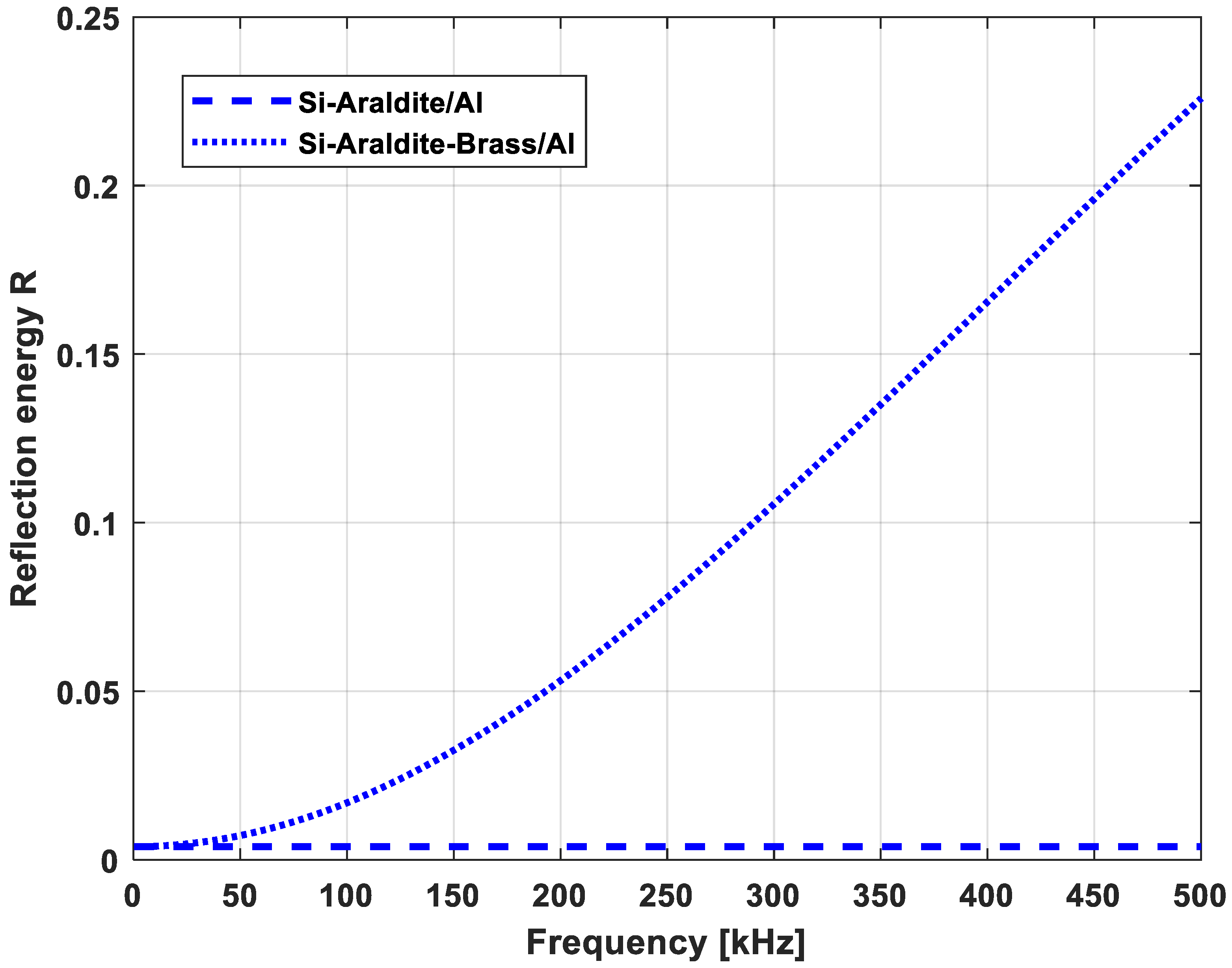
The working frequency band included the bandwidth of the CMUT-R100 (310–420 kHz) and the properties of each material used in the simulations are presented in
Table 2 [
23]. The evolution of the reflection coefficients as a function of frequency for Cases 1 and 2 is proposed in
Figure 10. Case 1 showed a very low reflection coefficient consistent with the micrometer thickness of the araldite and the acoustic impedances of silicon and aluminum of the same order of magnitude. However, the brass layer characterized by a millimeter thickness and an impedance mismatch with other layers implied significant losses increasing with the working frequency.
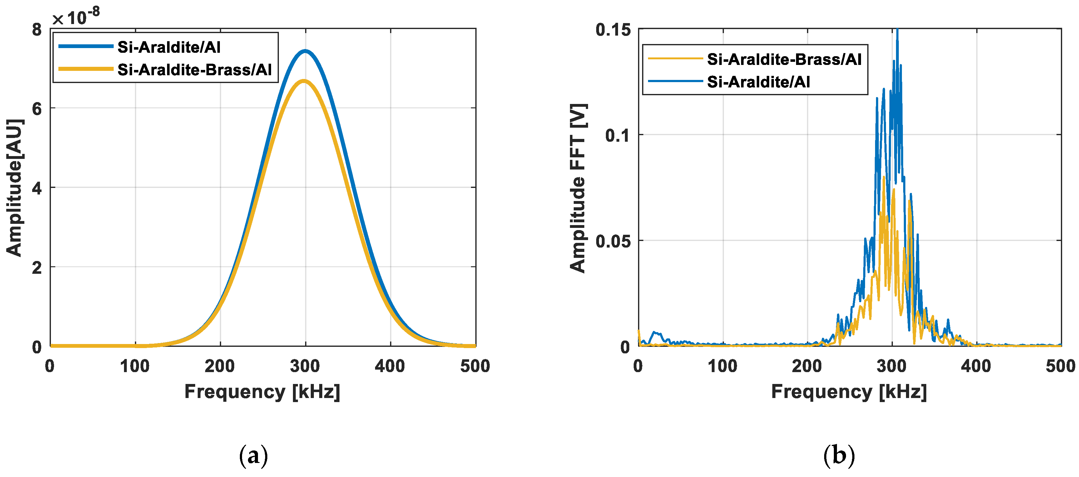
The amplitude of the transmitted as a function of frequency is shown in
Figure 11. In
Figure 11a, a virtual windowed sinusoid centered at 300 kHz with an arbitrary bandwidth was affected by the calculated transmission coefficient and in
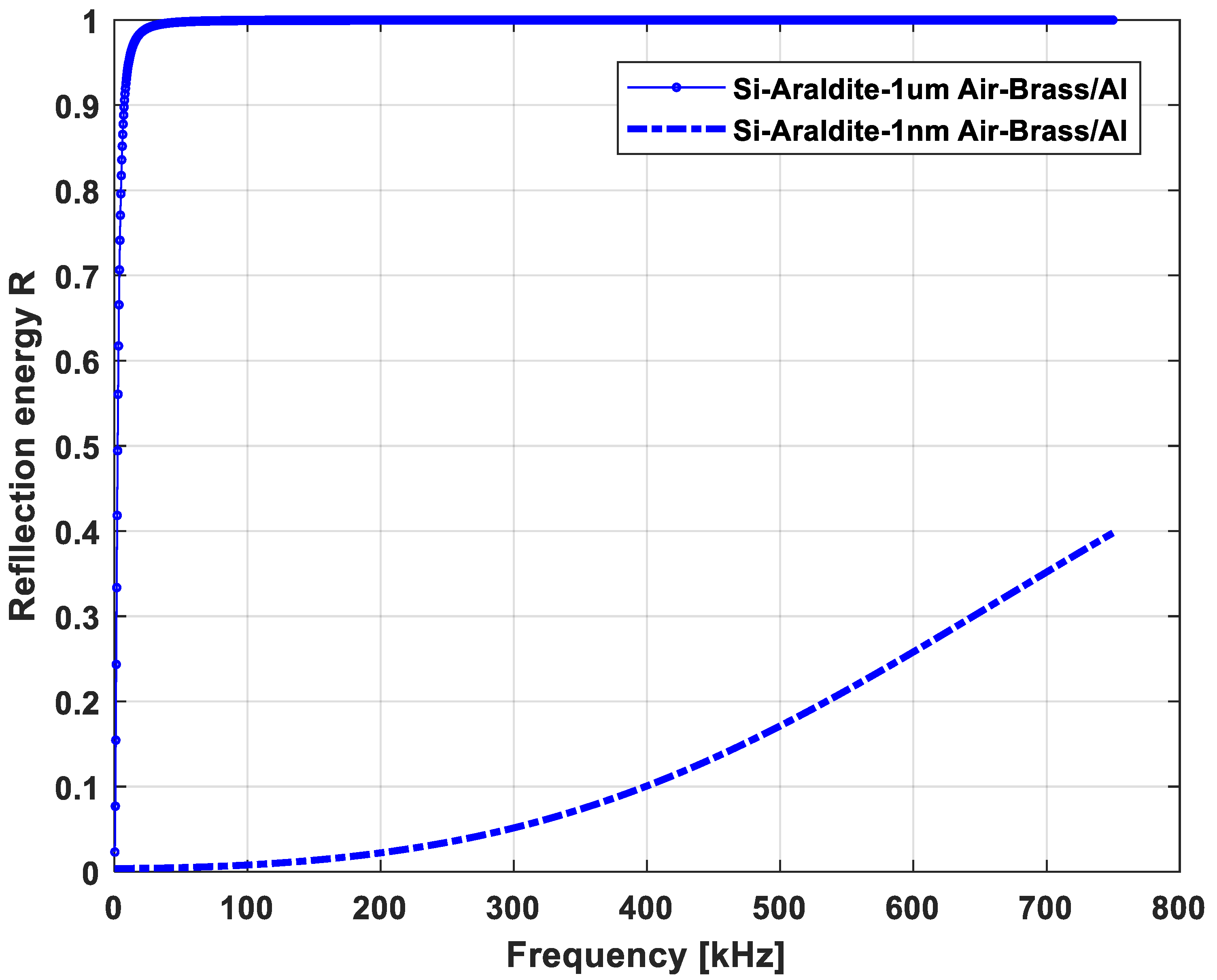
Figure 11b, the experimental data are reported. The attenuation between Case 1 and Case 2 of the detected signal was much greater for experimental data than for the theoretical evaluations, i.e., about 53% against 13%. The difference between the simulation and experimental results could be explained by the introduction of other defects such as material attenuation, air defect, and so on. In order to explain the influence of an air layer for example, Case 3 was considered with two air layer thicknesses of 1 nm and 1 µm. The simulation results presented in
Figure 12 show that even the thinnest air layers could cause significant losses at the interfaces. Surely, an air layer of 1 µm characterized by an almost total reflection of the propagating wave was overestimated. However, air layers of 1 nm or 10 nm are quite realistic and cause energy losses.
Thus, control of the acoustic coupling between each material is important to reduce insertion losses and to maximize the amplitude of the transmitted signal. Special attention must be paid to the bonding of the components of the CMUT-R100 sensor and its coupling with the monitored structure by minimizing air layers as much as possible.
3.2. Mechanical-Electrical Sensitivity
The mechanical-electrical contribution is related to the capacity of the elementary cell to convert the mechanical vibration of the suspended membrane into electrical charges and thus into electrical current. This is the subject of the following analytical developments.
3.2.1. Modeling
The capacitance
of the elementary cell can be expressed in terms of the initial electrostatic gap
and the total deflection
including a DC part
and an AC part
according to [
24]:
with
and where
and
are, respectively, the permittivity of vacuum or air, and the radius of the electrode (the radius of the electrode refers to the orange lower electrode in
Figure 1b,c). The DC part
is caused by the application of the DC bias voltage and the AC part
is the vibration amplitude induced by the incident elastic waves.
Considering that
, the total capacitance
for
Nc cells is expanded to the first order in
, i.e.,:
The electrical current
generated by the mechanical vibration is:
and thus,
A harmonic form of the AC part is assumed: with as a fit in accordance with the actual boundary conditions; i.e., clamped at the membrane radius with a vibration amplitude at the membrane center
Thus, the electric current becomes:
and finally, the mechanical-electrical sensitivity
can be written:
According to Equation (10), the mechanical-electrical sensitivity is mainly controlled by the electrode and membrane radii, the electrostatic gap between the upper and lower electrodes, and the VDC bias voltage.
The sensitivity of the Cooknell CA7 charge amplifier used, i.e., 250 mV/pC, defines the theoretical amplitude of the output voltage as follows:
Thus, the amplitude of the detected signal will preferentially be studied afterwards instead of the mechanical-electrical sensitivity considering one cell and a vibration amplitude of 1 nm, i.e., A(mV/nm/Nc).
3.2.2. Influence of the Surface Electrode on the Amplitude of the Detected Signal
In the studied configuration, the upper electrode consisted of the entire membrane made of a conductive layer “poly 2”. Only the bottom electrode deposited on the substrate and made of a conductive layer “poly 0” could be structured according to different radii. The electrode surface was given by the square of the ratio of the radius of the bottom electrode to that of the membrane. Based on the analytical developments of Nikoozadeh et al. [
25], the pull-in voltage and the static deflection
for a given
bias voltage were calculated with the dimensions and material properties described at
Section 2.1. The chosen
bias voltage, referred to as the corresponding DC voltage in the following, was considered to be equal to 60% of the pull-in voltage, i.e.,
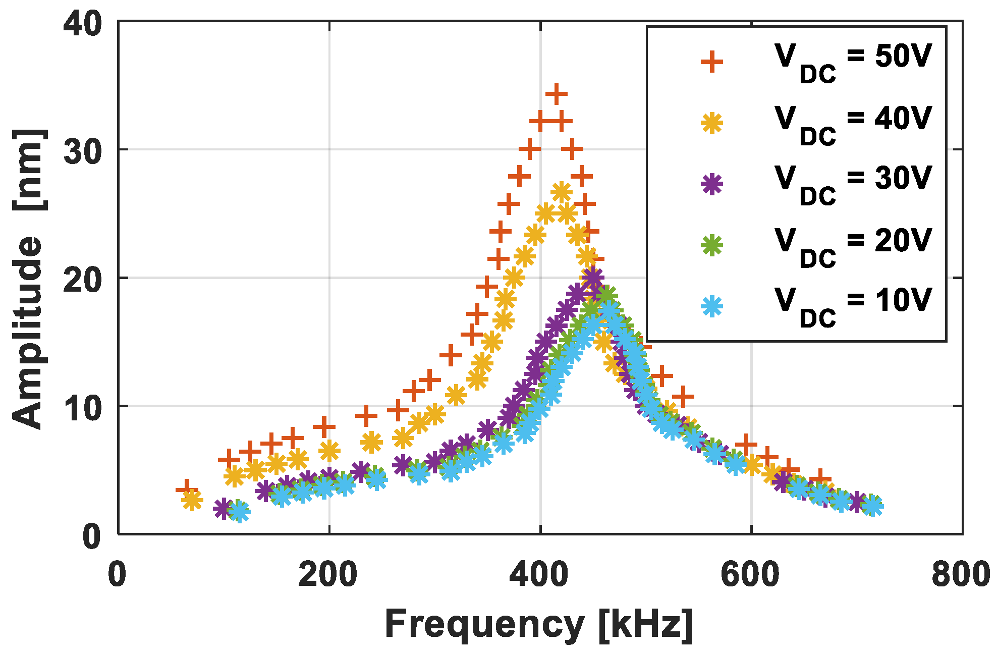
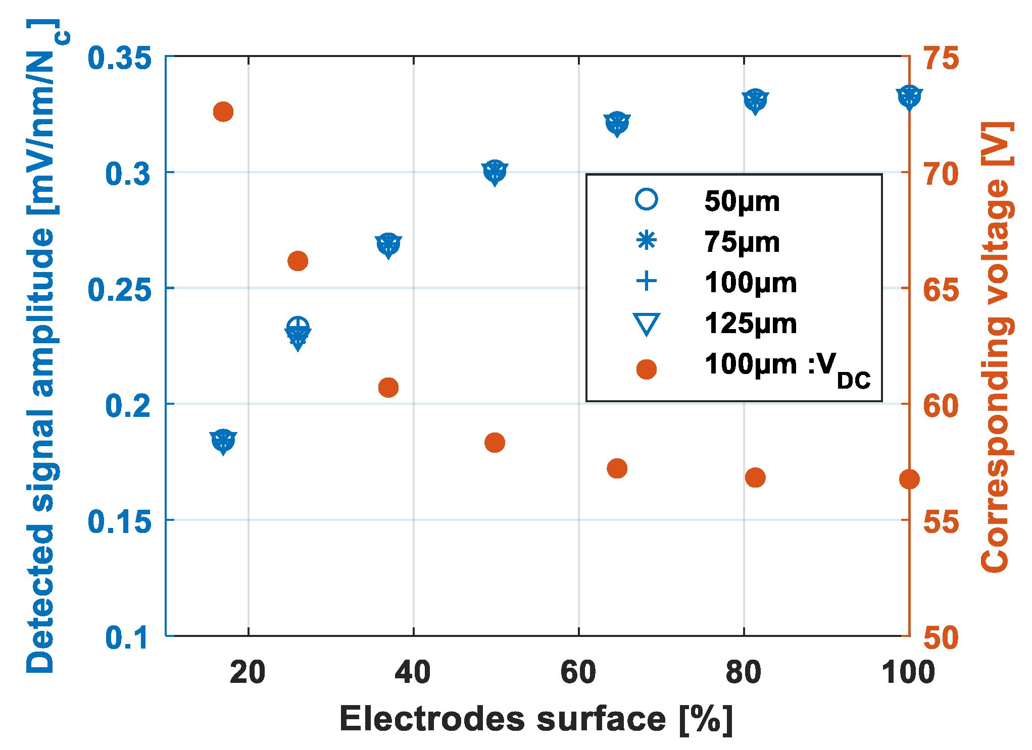
. Numerical simulations were performed with different membrane radii 50 µm, 75 µm, 100 µm and 125 µm.
Figure 13 shows that the evolution of the amplitude of the detected signal, which is to be read on the left-hand ordinate axis, did not depend on the membrane radius for a given electrode surface. This condition was not satisfied by the corresponding voltage. In
Figure 13, referring to the right-hand ordinate axis, the corresponding DC voltage is shown only for the 100 µm radius membranes which were the components of the CMUT-R100 sensor. Thus, for the 100 µm radius membranes, the amplitude of the detected signal and the corresponding voltage increased and respectively decreased to asymptotic values around 0.33 mV and 57 V, respectively, from electrode surface values of the order of 65%, i.e., an electrode radius around 80% of that of the membrane. It can already be deduced that an electrode radius of 80% can be considered as the optimum value [
26], because beyond this, only the parasitic capacitances increased. Considering the asymptotic value of the detected signal and that
, the amplitude of the detected signal can be evaluated for an electrodes surface of 100% by integration of Equation (11):
with
α the fraction of the pull-in voltage
3.2.3. Influence of the DC Bias Voltage on the Amplitude of the Detected Signal
Considering the DC bias voltage as a fraction of the pull-in voltage, the first step is to determine the pull-in voltage according to the mechanical and geometrical parameters. Zhang et al. [
27] developed an analytical model to calculate the pull-in voltage of a flat circular CMUT cell with a sealed cavity. In the present case, the CMUT cell is perforated, resulting in a pressure balance between the cavity and the surrounding medium. The formula (considering a pressure difference
) gives the voltage for the ratio
as follows:
with
The pull-in voltage is obtained when
V is maximal and hence when
f(x) is maximal. As
Equation (14) has been validated by a very good correlation, i.e., a maximum relative error of 1.2%, with numerical simulations taking into account various mechanical properties and geometrical parameters (gap, thickness and membrane radius). Combining Equations (12) and (14), the amplitude of the detected signal for 1 nm of center vibration amplitude
of the membrane can be written as:
Equation (15) is based on the assumption that the static deflection
is small relative to the electrostatic gap
g. However, this assumption is even less valid the closer the DC voltage is to the pull-in one; which is the case for the optimization of the sensor sensitivity.
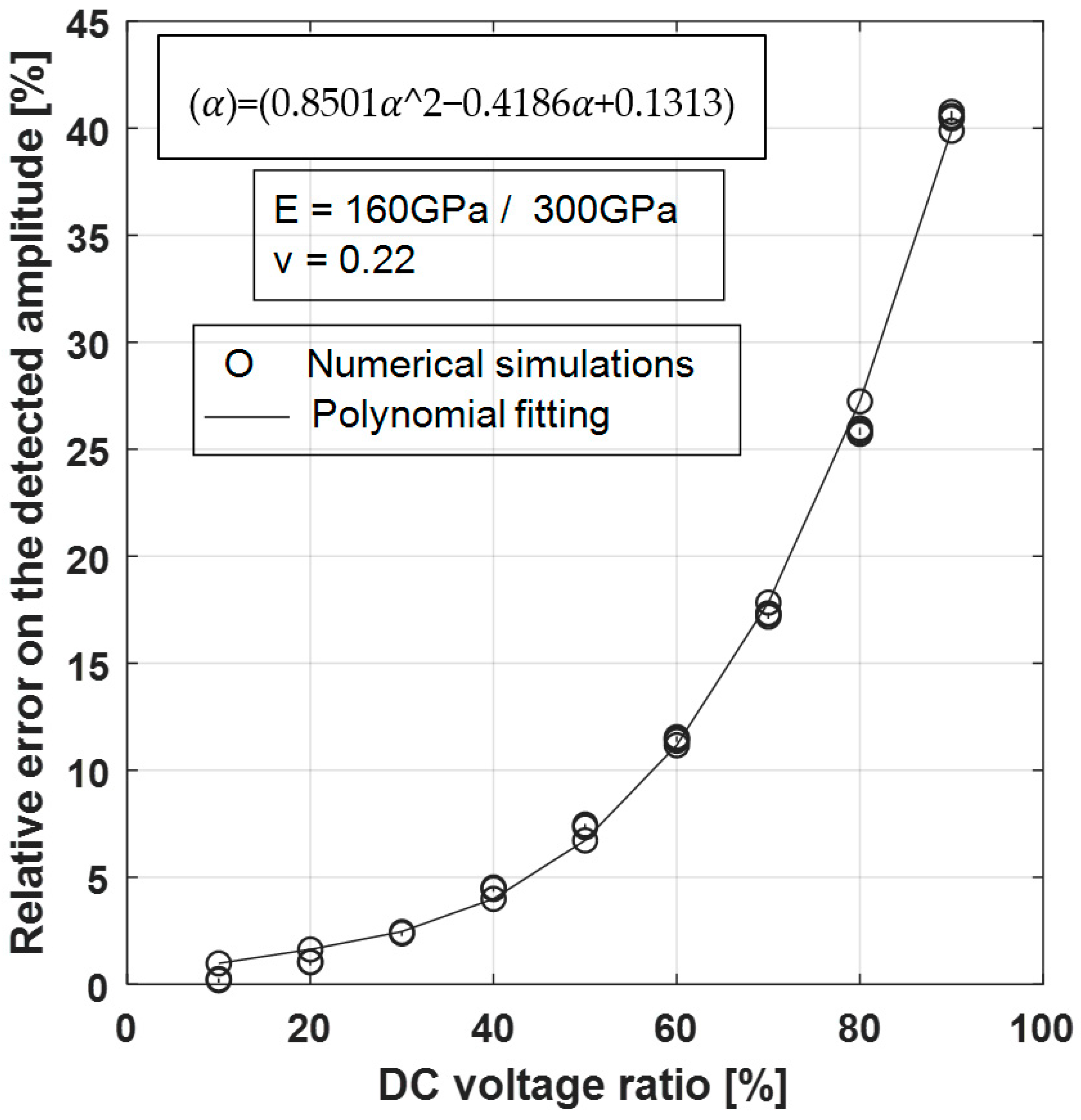
Figure 14 shows that the relative error on the amplitude of the detected signal exceeded 10% from a DC voltage ratio
of 60%, reached 25% for 80% ratio and then 40% for 90% ratio.
A large set of points (i.e., 600 points per DC voltage ratio) was considered to scan the material properties (160 GPa for polysilicon and 300 GPa for silicon nitride) and geometrical parameters (gap from 0.5 µm to 5 µm, thickness from 0.5 µm to 3 µm and membrane radius from 30 µm to 120 µm) within a “realistic” range. It can be seen that the relative errors seemed to only depend on the DC voltage ratio; which made it possible to envisage a third-degree polynomial fitting. Thus, the amplitude of the detected signal can be accessed accurately with a relative error of less than 1.2% by the following analytical expression:
with
,
α representing the DC voltage ratio.
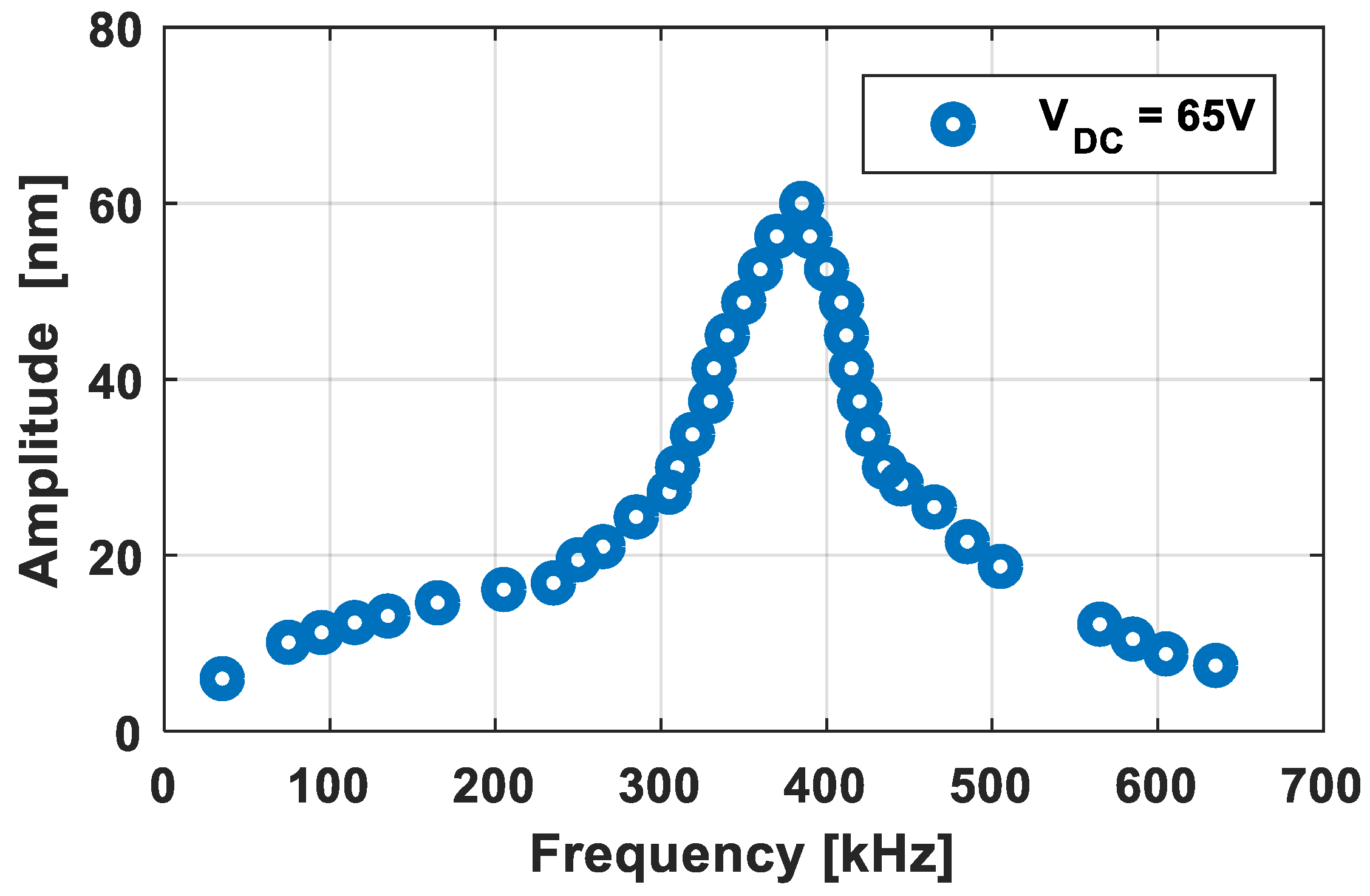
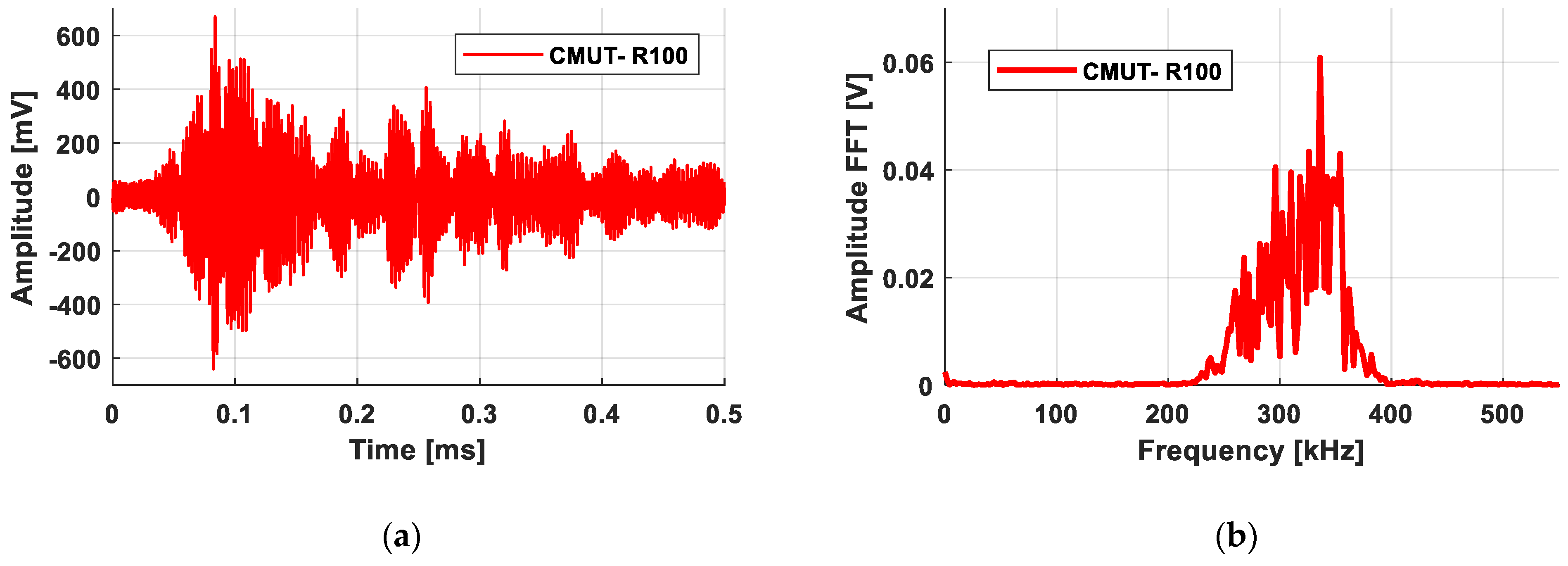
A numerical application of Equation (16) considering 65 VDC (80% of VPI), 40 elementary cells, geometrical parameters and material properties of the manufactured membranes gives for the acoustic emission test an amplitude of the detected signal about 20 mV for a vibration amplitude of 1 nm. Thus, the measured signal amplitude of about 700 mV leads by Equation (16) to about 35 nm vibration amplitude, which is a realistic value in this context.
3.2.4. Optimization Ways: Trends for Future Works
According to Equation (16), the amplitude of the detected signal and thus the sensitivity of the sensor can be estimated in the dimensioning phase and some ways of optimization are highlighted as follows: smaller electrostatic gaps g, larger thicknesses t, a stiffener membrane material E/(1−ν2) and a higher DC voltage ratio α.
If the electrical parameter α was already studied for the CMUT-R100 sensor, the geometrical and material parameters cannot be modified so easily from a given micromanufacturing process. One the one hand, there is a small technological capacity for change: in the case of MUMPS process, the constituent material is polysilicon, with two possible polysilicon layers Poly 1 (2 µm) and Poly 2 (1.5 μm) and two possible oxide layers defining the gaps Oxide 1 (2 µm) and Oxide 2 (0.75 μm). On the other hand, each technological change in thickness or gap requires a new fabrication run. Only the in-plane dimensions, mainly the membrane radius, can be directly scanned by the modification of the mask design.
Thus, the optimization of sensitivity should be thought about comprehensively by investigating new manufacturing processes that can be the subject of future work in the longer term. These should aim at simultaneously optimizing material, geometrical and electrical parameters.
Concerning the material properties, silicon nitride is a good candidate to replace polysilicon. Silicon nitride is already involved in CMUT fabrication [
28] and its material properties (similar Poisson’s ratio and higher Young modulus: around 0.25 and 300 GPa, respectively, [
29]) could improve, according to Equation (16), the amplitude of the detected signal by a factor of ≈1.4 compared to polysilicon.
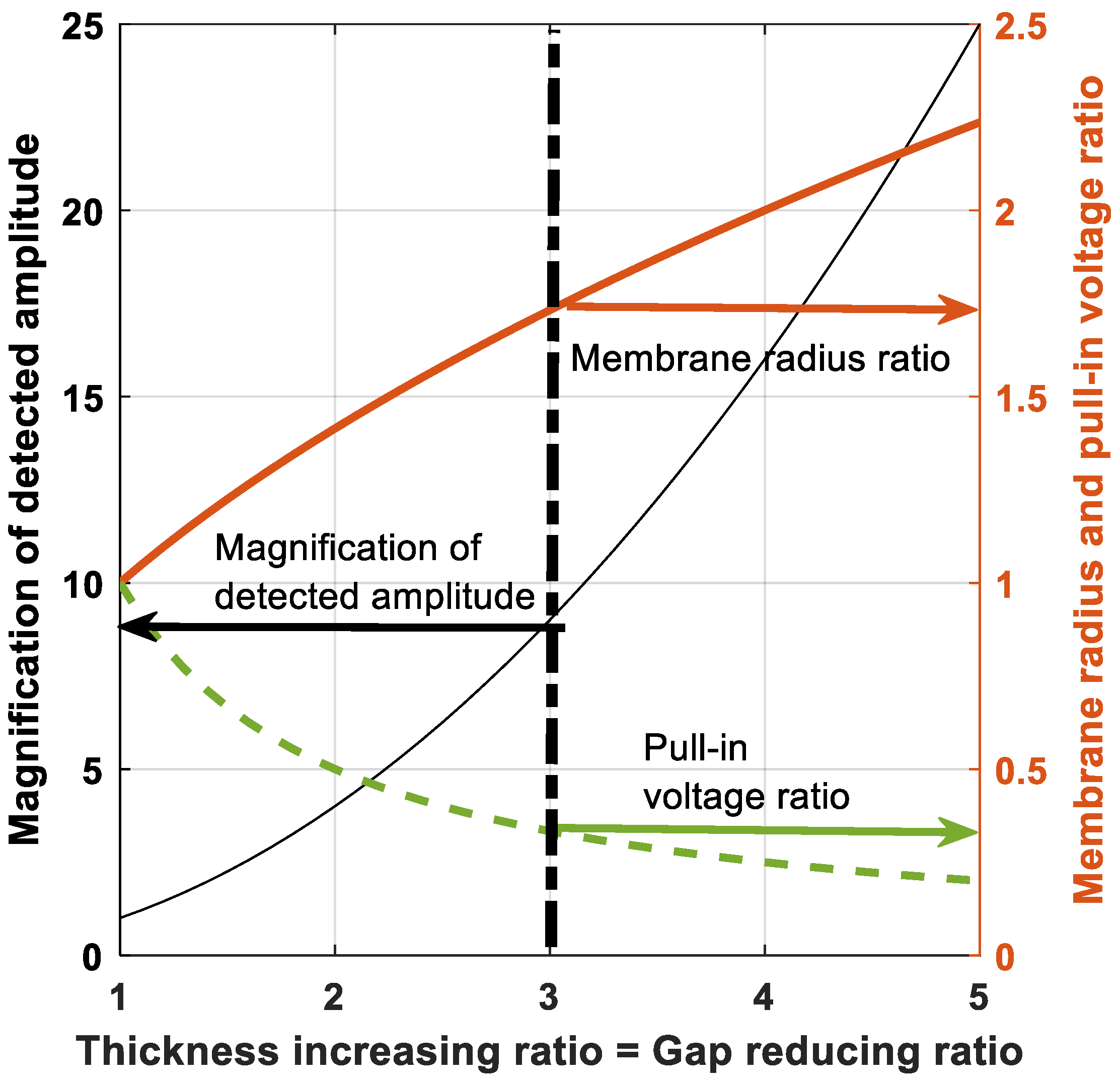
To illustrate the possible magnification of the detected amplitude related to the geometrical parameters, it is assumed that the membrane thickness and the electrostatic gap can be affected by an inverse ratio; for example, the thickness is multiplied by
k (increasing ratio) and the gap is divided by
k (decreasing ratio). According to Equation (16), the magnification
M evolves like the square of
k (see
Figure 15).
Figure 15 highlights a realistic ratio of 3 (in this context, the thickness and the gap would be respectively about 4 µm and 0.7 µm) which leads to a detected amplitude 9 times higher. Furthermore, the resonant frequency
f of a circular membrane is proportional to the thickness and inversely proportional to the square of membrane radius (Equation (1) in [
7]). Thus, to maintain a given resonant frequency, the membrane radius must be modified according to the square root of the ratio
k.
Lastly, according to Equation (14), the pull-in voltage is proportional to the product of the thickness and gap and inversely proportional to the square of the membrane radius. Thus, changing the membrane radius results in a reduction of the pull-in voltage by a factor equal to the ratio
k. The evolutions discussed above and shown in
Figure 15 can be summarized as follows:
The parameters with “ref” in superscript correspond to the reference values of thickness, gap, detected amplitude, resonant frequency, membrane radius and pull-in voltage related to a given design and the resulting electromechanical characteristics.
4. Conclusions and Perspectives
In this paper, several lines of research have been undertaken to analyze and optimize the signal-to-noise ratio and especially the sensitivity of CMUT-based sensors dedicated to AE applications: the design, packaging and electrical connections of the sensor, the processing of the detected signal, the acoustic coupling conditions at the interfaces of the layered sensor structure and the design and operating conditions of the elementary cells.
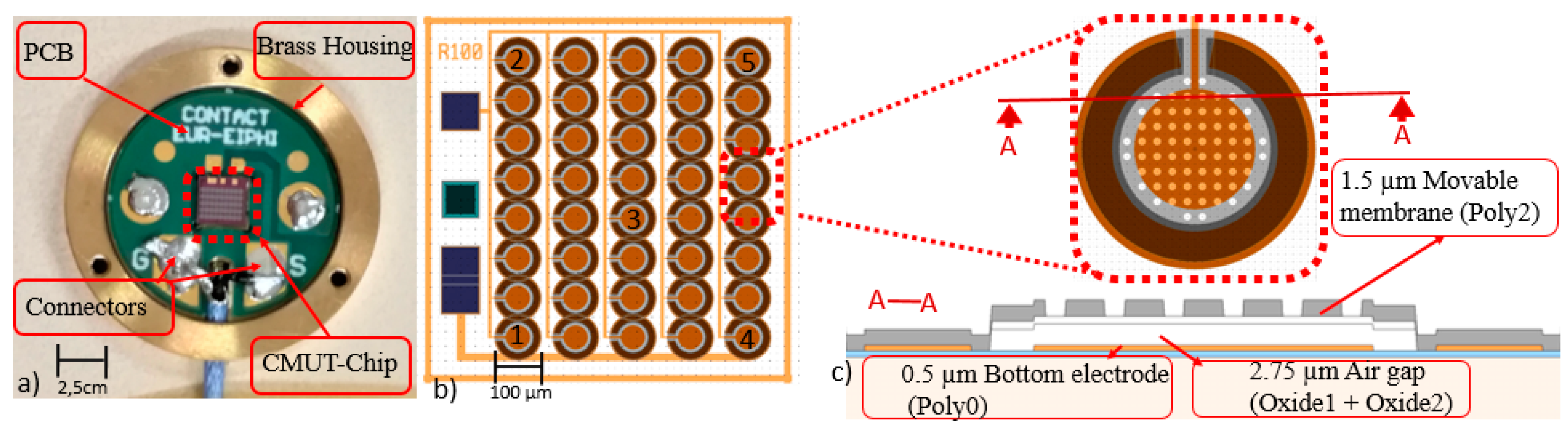
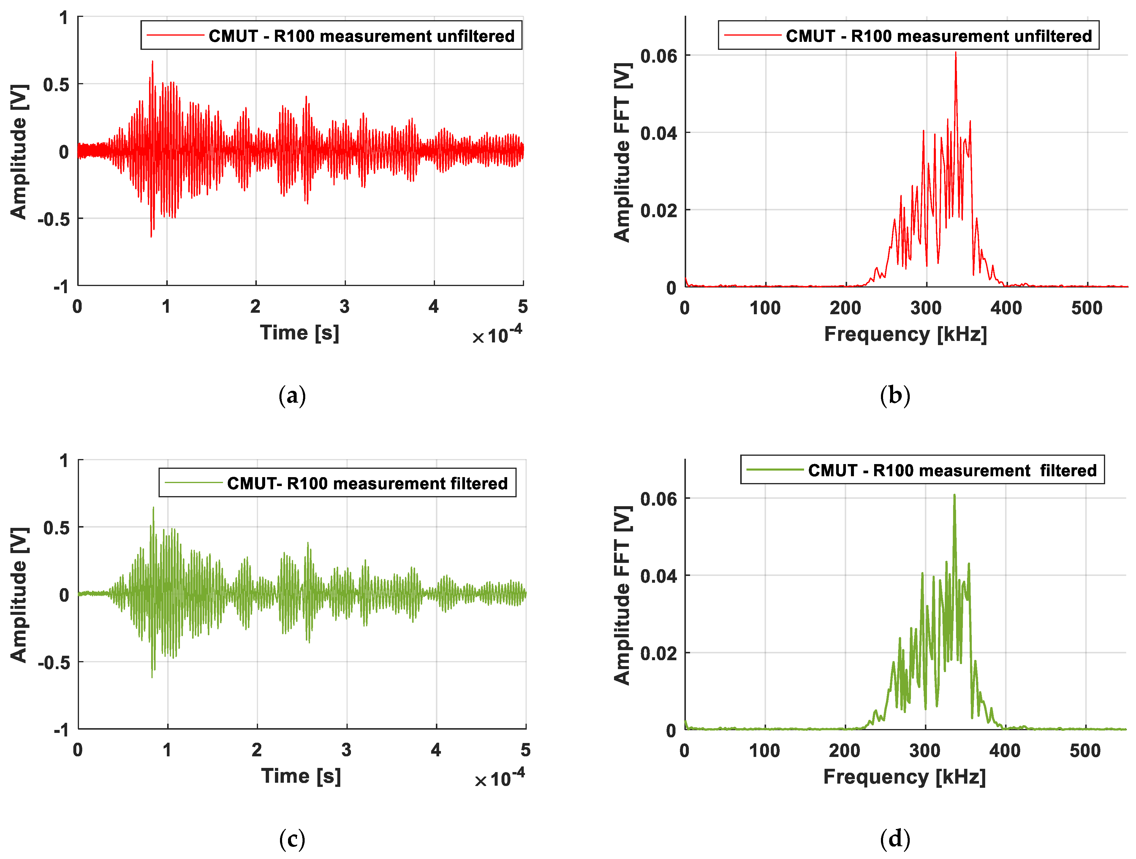
The CMUT-R100 sensor based on previous works was developed, considering reduced sizes of the chip (2.5 mm × 2.5 mm) and the overall sensor (16 mm in diameter and 1.6 mm in height) and a higher number of elementary cells (40). The operating conditions in terms of DC bias voltage and frequency range of the elementary cells were respectively determined around 65 V and 310 kHz–420 kHz. The CMUT-chip was wire bonded on a PCB which was implemented in a brass housing to be tested on an aluminum sample instrumented by a piezoelectric transmitter simulating acoustic emission. The new design and packaging, the care taken to the electrical connections and the simple processing of the detected signal have contributed to increase the signal-to-noise ratio from 17 dB to 37 dB.
To go further, the sensitivity of the sensor was then analyzed in two parts: one acoustic-mechanical and other mechanical-electrical. Concerning the acoustic-mechanical part, experimental tests and the calculation of the acoustical impedance of layered structures showed the influence of insertion losses at the different interfaces.
It is essential to reduce to a minimum the layer thicknesses characterized by a poor matching of the acoustic impedance to the adjacent layers. In particular, air layers should be thinned as much as possible for example by exerting sufficient bonding pressure when bonding cannot be avoided.
The study of the mechanical-electrical part allowed the analytical definition of the amplitude of the detected signal from the geometrical parameters, the material properties, the operating conditions and the charge amplifier used. A first attempt to correlate the experimental amplitude of the detected signal and the closed-form solution gave a vibration amplitude of the CMUT cell of about 35 nm, where tens of nanometers were usually expected.
From Equation (16), the key elements of the design should be noted: the independence of the cell radius, design of a membrane with a large thickness and a small electrostatic gap, choice of a membrane material with a high Young modulus and operation at DC bias voltage as close as possible to the pull-in voltage. Membrane thickness, electrostatic gap and membrane material are parameters, which depend on the selected manufacturing process. For example, the MUMPS process has predefined steps with specific material layers and a too limited range of thicknesses and gaps. Thus, the study of a wider range of parameters leads to challenging work in the longer term as it requires the use of clean room microfabrication facilities to develop or codevelop inhouse manufacturing processes.
Future shorter-term work on this aspect will rather aim at extending the study of the mechanical-electrical sensitivity to other geometrical forms of membranes and possibly to other structures and/or boundary conditions. An aspect not treated in this context, the quality factor of vibrating membranes, is also a working perspective since it conditions the acoustic-mechanical sensitivity. The quality factor could depend on the geometrical shapes of membranes, the boundary conditions but also on geometrical parameters such as the radius and thickness of the membranes. Finally, regarding the practical aspects, the signal processing could be handled by a hardware solution for the CMUT-R100. On the other hand, other sensors as CMUT-R50, CMUT-R75 and CMUT-R150 could be designed and manufactured in the near future to cover a wider bandwidth from 150 kHz to 2000 kHz which is of practical interest for structural health monitoring.


