A Preliminary Study on Non Contact Thermal Monitoring of Microwave Photonic Systems †
by
 , and
, and
Bushra Jalil
*, 
Bilal Hussain
,
Maria Antonietta Pascali
,
Giovanni Serafino
,
Davide Moroni
 and
and
Paolo Ghelfi
Istituto di Scienza e Tecnologie dell’Informazione “Alessandro Faedo” CNR, 56124 Pisa, Italy
*
Author to whom correspondence should be addressed.
†
Presented at the 15th International Workshop on Advanced Infrared Technology and Applications (AITA 2019), Florence, Italy, 17–19 September 2019.
Proceedings 2019, 27(1), 19; https://doi.org/10.3390/proceedings2019027019
Published: 23 September 2019
(This article belongs to the Proceedings of The 15th International Workshop on Advanced Infrared Technology and Applications)
Abstract
:Microwave photonic systems are more susceptible to thermal fluctuations due to thermo-optic effect. In order to stabilize the performance of photonic components, thermal monitoring is achieved by using thermistors placed at any arbitrary location along the component. This work presents non contact thermography of a fully functional microwave photonic system. The temperature profile of printed circuit board (PCB) and photonic integrated circuit (PIC) is obtained using Fluke FLIR (A65) camera. We performed Otsu’s thresholding to segment heat centers located across PCB as well as PIC. The infrared and visible cameras used in this work have different field of view, therefore, after applying morphological methods, we performed image registration to synchronize both visible and thermal images. We demonstrate this method on the circuit board with active electrical/photonic elements and were able to observe thermal profile of these components.
1. Introduction
Microwave photonic systems are increasingly used for communication and sensing applications. The ever-increasing demand of speed and high frequency (beyond 60GHz) usage for communication has sparked the interest in utilizing photonic techniques for radio frequency (RF) applications. Recent introduction of silicon photonics has provided the opportunity to integrate electronic and photonic systems using a common material. Heating from different signals can cause an increase in the temperature of the electronic and photonic circuits which can have significant impact on the performance and reliability of the photonic chip. As the photonics systems operate at 100 s of THz, their performance remains stable over whole RF band (0.3–100 GHz). Most photonic components such as phase shifters, modulators and filters rely on the use of thermo-optic effect. In order to tune the device for desired specification, the temperature profile is strictly measured and stabilized using thermo-electric coolers (TECs). Conventionally, temperature is monitored using miniaturized thermistors. Though, the modern thermistors can accurately measure the temperature locally of a device under test (DUT), yet a complete thermal profile cannot be obtained due to the fact that placement of thermistor is not strictly controlled. Moreover, the heat dissipation in silicon devices is dependent on the number of devices and metal across the PIC. Non contact thermal imaging has gained recognition in the field of electronic and power systems during the last two decade [1,2,3]. It has been widely used for fault monitoring of different electronic circuits and also for the preventive maintenance work. Infrared imaging uses infrared sensors to estimate heat emissivity of objects based on black body radiation. The IR-camera records the detected IR wavelengths radiated from the objects in its field-of-view. The recorded IR wavelengths correspond to various temperatures based on the Planck’s law of black body radiation. In general, thermal imaging is considered as a robust, non-destructive and contact less methodology as images are visualized directly on the camera’s display. Furthermore, for the automated board inspection, the camera can be controlled by a remote PC via different standard interfaces.
In this work, we study the heat profile of electronic and photonic components using Infrared (IR) camera by Fluke (FLIR A65). An RF beam-steering system based on microwave photonic techniques [4] is monitored. The beam-steering system is comprised of PIC and various discrete electronic components such as amplifiers, filters, current sources and comparators mounted on a multilayer PCB. Using innovative image processing techniques, various heat centers across the PIC and PCB are observed. Moreover, the heat profile of PIC is obtained separately using the zoom of FLIR camera. In the next coming section, we will explain the experimental setup, methods and obtained results.
2. Methods
Thermal and Infrared imaging is a technique commonly used to test and inspect electronic components. The thermal effects are one of the main limiting factors in electronic equipment operation and their thermal behavior is necessary to detect their possible failures and to enhance their reliability. In this work, we performed thermal imaging to identify and monitor heat centers/traps on princted circuit boards. In order to know the component type from visible image, we decided to apply multi-modal image processing, and to perform image fusion by registering both visible and IR images prior to segmentation. Image registration is a mapping between two or more images both spatially (geometrically) and with respect to intensity. Kim et al., presents a description and methods to perform registration [5]. Mathematically, registration is expressed as [6]:
where and are two-dimensional images (indexed by ), ↦ maps the indices of the distorted frame to match those of the reference frame, and g is intensity or radiometric transform. Various techniques have been used to classify anomalies in the infrared image of electrical equipment, and among those, the qualitative measurement is widely used. This qualitative measurement is based on the relative threshold criteria termed as comparative analysis. In order to extract the heat source within the IR image, we segment the image based on Otsu’s thresholding [7].
where, T represents the threshold value and represent the segmented image.
3. Results
3.1. Data Acquisition
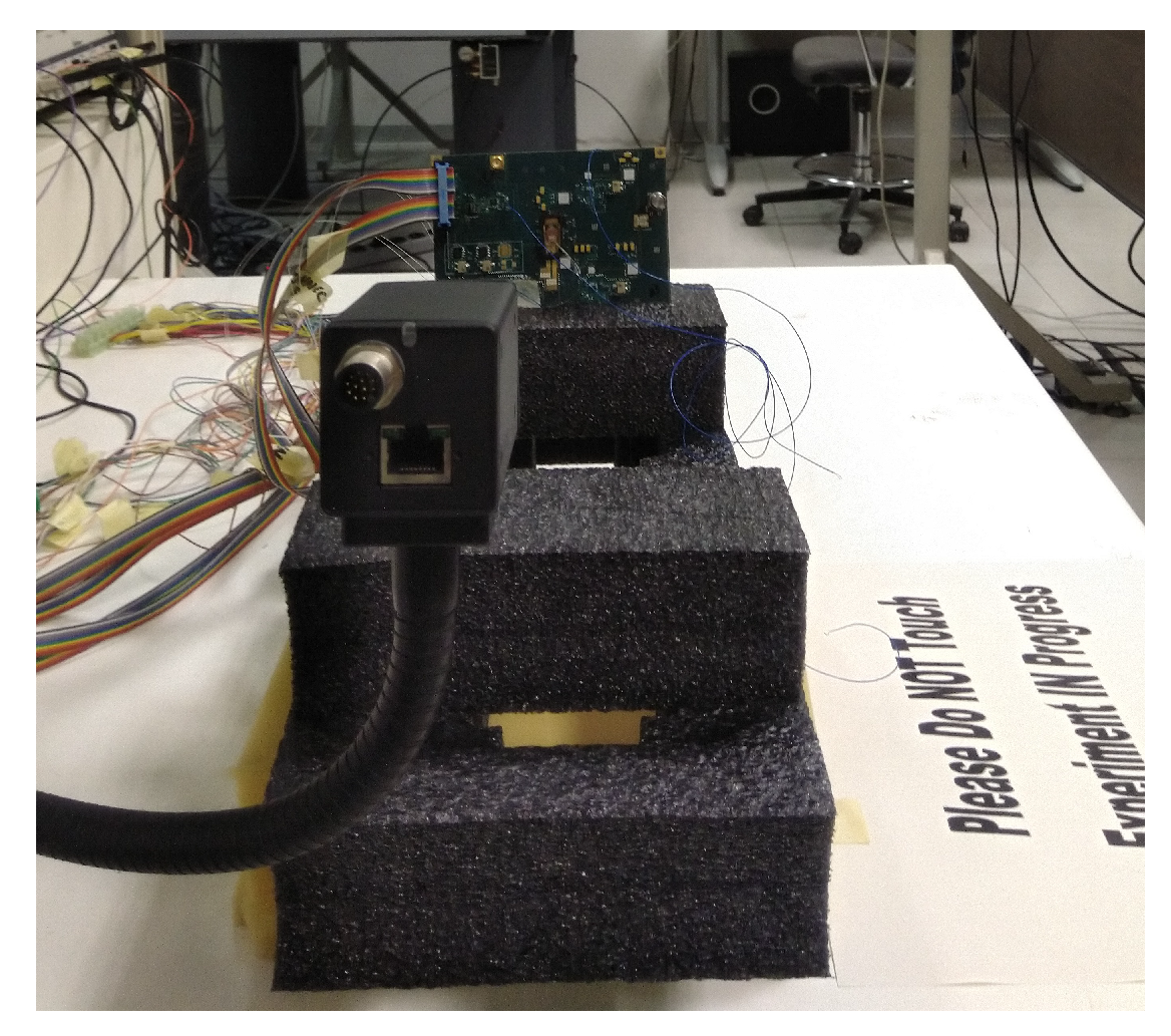
The experimental setup is shown in Figure 1. Infrared data and images in the visible spectrum have been acquired under different conditions as shown in Table 1. The data was acquired at the frame rate (about 5 f/s) with the infrared camera: FLIR A65sc with the standard lens (25 mm focal length H-FOV × V-FOV = 25× 20). In order to map the heat profile of 4-layer Rogers 4350 b PCB (size 8 × 11.5 cm) containing electronic as well as photonic components, the FLIR camera is mounted at a distance of 0.384 m while keeping the whole system in a thermally insulated container (to avoid external heat sources). The experiments were performed on both sides of PCB and total of 15 sequences (SEQ) of images were acquired at first. At the second stage of experiment, we provide external heat source and study the thermal behaviour of PIC only.
3.2. Experimental Results
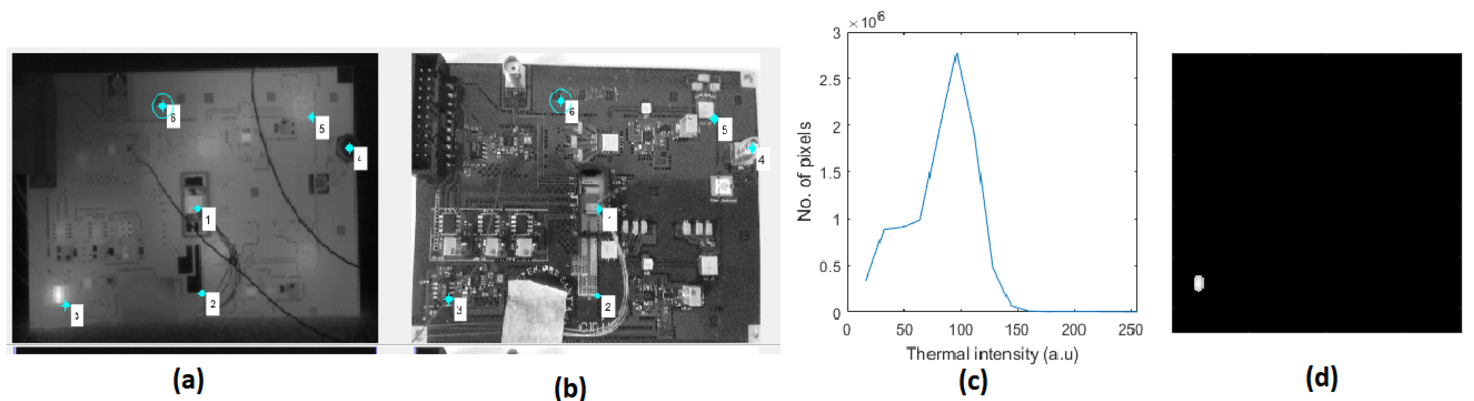
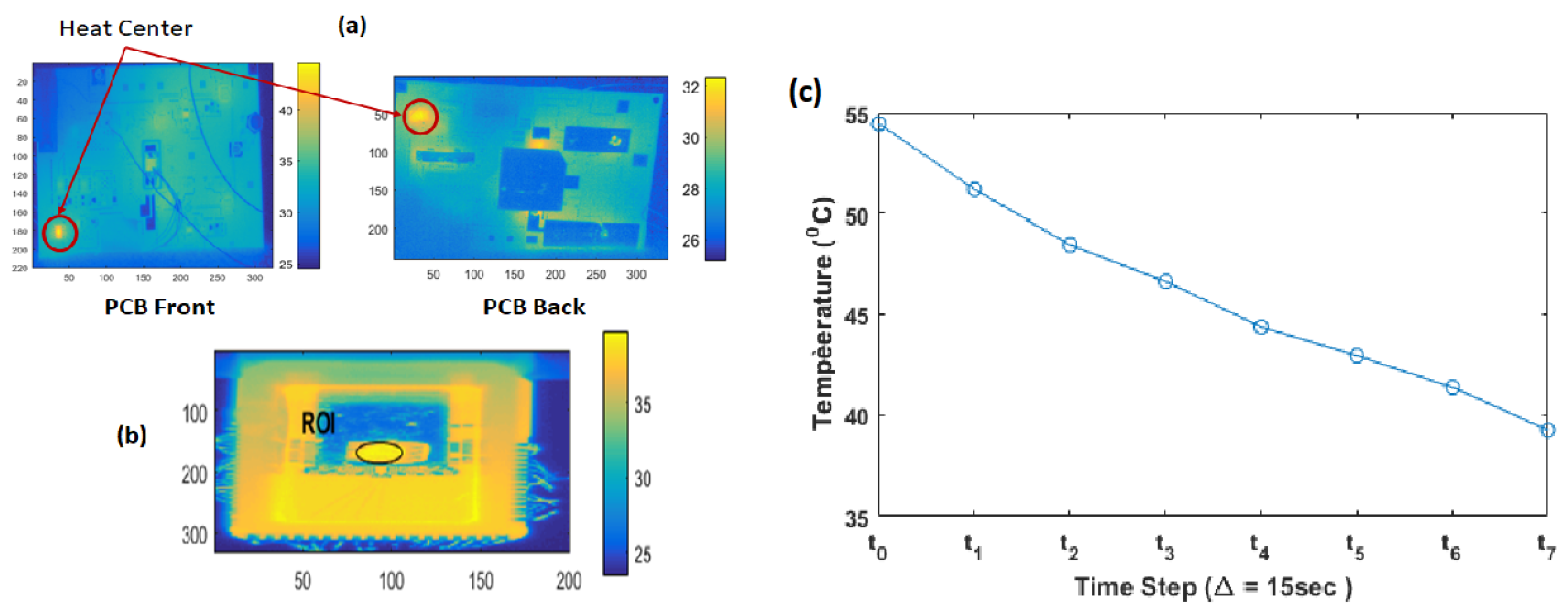
We applied histogram based thresholding on the recorded IR image as shown in Figure 2a. As both visible and infrared images are registered, therefore the spatial placement of different electronic and photonic components are known. By using the Otsu’s threshold based segmentation on the histogram of thermal profile, we were able to highlight the temperature profile of PIC as shown in Figure 2c,d. Using image processing, a color-coded thermal profile is obtained in Figure 3a. It can be observed that there exist heat centers with temperature in the range of 60 C. Upon comparing with the layout of PCB, it was observed that similar device was used in another location of PCB. The absence of other heat center owes to the fact that heat transfer is provided by a wide metal strip in the bottom layer of PCB. Presence of such heat centers can reduce the life-time of electronic device by almost 25%. This kind of heat traps can be avoided by using a careful PCB layout. Moreover, for obtaining the heat profile of silicon-based PIC, an external uniform heat source was applied to the bottom of the PIC. The obtained color-coded heat profile Figure 3b shows that heat transfer across PIC is non-uniform. By using a TEC, it is not possible to stabilize the temperature across the silicon die uniformly in a short-span. This in-turn provides the ability to predict the tunability speed of various photonic components on the chip. Such information is vital for speed critical applications. At the second stage, we increase the temperature of PIC to some extent by using external heat source and observed the decline of temperature with different steps of time. The curve in Figure 3c shows the behaviour with an approximate time step of 15 s.
4. Conclusions
This work presents the preliminary study to investigate the thermal profile of photonic integrated circuits. The acquired visible and IR images were analyzed through computer vision methods to segment heat sources and critical overheating components on the circuit board. We observed that the temperature profile of photonic components were linearly declined during a period of time. In conclusion, the IR testing of photonic chip temperature is the only method for non-destructive testing. Furthermore, for the automated board inspection by generating thermal map, the camera can be controlled by a remote PC via different standard interfaces. The temperature monitoring of RF amplifiers can also help in determining dynamic noise figure.
Conflicts of Interest
The authors declare no conflict of interest.
References
- Wagh, C.R.; Baru, M.V.B. Detection of Faulty Region on Printed Circuit Board With IR Thermography. Int. J. Sci. Eng. Res. 2013, 4, 4. [Google Scholar]
- Petrosyants, K.; Kharitonov, I. Non-destructive testing of electronic components overheating using infrared thermography. Proceedings of The VIII-th International Workshop on NonDestructive Test (NDT) in Progress 2015, Prague, Czech Republic, 12–14 October 2015; Brno University of Technology: Brno, Czech Republic, 2015; Volume 3. [Google Scholar]
- Breitenstein, O. Lock-in IR Thermography for Functional Testing of Electronic Devices. In Proceedings of the Vortrag 7th Int. Conf. on Quantitative Infrared Thermography, Sint-Genesius-Rode, Belgium, 5–8 July 2004; pp. 1–6. [Google Scholar]
- Amato, F.; Serafino, G.; Hussain, B.; Toccafondo, V.; Chiesa, M.; Scotti, F.; Porzi, C.; Bogoni, A.; Ghelfi, P. Ultra-Fast Beam Steering of a Phased-Array Antenna Based on Packaged Photonic Integrated Circuits. In Proceedings of the 2018 European Conference on Optical Communication (ECOC), Rome, Italy, 23–27 September 2018. [Google Scholar]
- Kim, K. Survey on Registration Techniques of Visible and Infrared Images. IT Converg. Ractice (INPRA) 2015, 3, 25–35. [Google Scholar]
- Hines, G. Multi-Image Registration for an Enhanced Vision System; NASA Langley Research Center: Hampton, VA, USA, 2003.
- Otsu, N. A threshold selection method from gray-level histograms. IEEE Trans. Syst. Man Cybern. 1979, 9, 62–66. [Google Scholar] [CrossRef]
Figure 1.
Experimental Setup.

Figure 2.
(a) Thermal profile of circuit board front (b) Obtained image with visible camera to understand the spatial position of different components, (c) Histogram of thermal profile, (d) Segmented high heat area.
Figure 2.
(a) Thermal profile of circuit board front (b) Obtained image with visible camera to understand the spatial position of different components, (c) Histogram of thermal profile, (d) Segmented high heat area.

Figure 3.
(a) color-coded thermal profile of circuit board, front and back, (b)Region of Interest (ROI), photonic component., (c) Obtained Graph of Photonic chip, Distance Camera to target = 8 cm, emissivity= 1 and with time step of 15 s.
Figure 3.
(a) color-coded thermal profile of circuit board, front and back, (b)Region of Interest (ROI), photonic component., (c) Obtained Graph of Photonic chip, Distance Camera to target = 8 cm, emissivity= 1 and with time step of 15 s.


Table 1.
Different conditions to observe thermal profile of PCB and associated components.
| SEQ | Board | Temperature | Switch |
|---|---|---|---|
| 1–3 | Front | decreasing | OFF |
| 4–5 | Front | stable | OFF |
| 6 | Back | stable | OFF |
| 7–10 | Back | increasing | ON |
| 11–12 | Front | stable | ON |
| 13–15 | Front | decreasing | OFF |
Publisher’s Note: MDPI stays neutral with regard to jurisdictional claims in published maps and institutional affiliations. |
© 2019 by the authors. Licensee MDPI, Basel, Switzerland. This article is an open access article distributed under the terms and conditions of the Creative Commons Attribution (CC BY) license (https://creativecommons.org/licenses/by/4.0/).
Share and Cite
MDPI and ACS Style
Jalil, B.; Hussain, B.; Pascali, M.A.; Serafino, G.; Moroni, D.; Ghelfi, P. A Preliminary Study on Non Contact Thermal Monitoring of Microwave Photonic Systems. Proceedings 2019, 27, 19. https://doi.org/10.3390/proceedings2019027019
AMA Style
Jalil B, Hussain B, Pascali MA, Serafino G, Moroni D, Ghelfi P. A Preliminary Study on Non Contact Thermal Monitoring of Microwave Photonic Systems. Proceedings. 2019; 27(1):19. https://doi.org/10.3390/proceedings2019027019
Chicago/Turabian StyleJalil, Bushra, Bilal Hussain, Maria Antonietta Pascali, Giovanni Serafino, Davide Moroni, and Paolo Ghelfi. 2019. "A Preliminary Study on Non Contact Thermal Monitoring of Microwave Photonic Systems" Proceedings 27, no. 1: 19. https://doi.org/10.3390/proceedings2019027019