3DInkPack—Inkjet Printing of Discrete Sensor Packages for Advanced Rapid Prototyping †


CTR Carinthian Tech Research AG, Europastrasse 12, A-9524 Villach, Austria
*
Author to whom correspondence should be addressed.
†
Presented at the Eurosensors 2017 Conference, Paris, France, 3–6 September 2017.
Proceedings 2017, 1(4), 609; https://doi.org/10.3390/proceedings1040609
Published: 29 August 2017
(This article belongs to the Proceedings of Proceedings of Eurosensors 2017, Paris, France, 3–6 September 2017)
Abstract
:A rapid advanced packaging concept, consisting of inkjet photopolymer printing and Ag nanoparticles printing, was investigated for the construction of a pressure sensor package. Acrylate-type 3D package housing with 7 through-holes was printed with a polyjet printer and the through-vias and connection pads were manufactured via Ag glue dispensing and inkjet printing of Ag nanoparticle ink. The flip-chip packaging concept was pursued for the electrical connection between the package and the pressure sensor dye.
1. Introduction
Recent advances and development of microelectromechanical systems (MEMS), micro-opto-electro-mechanical systems (MOEMS), microelectronic products, and their tendency toward miniaturization has led to an urgent need for improvement in the micro- and/or nanofabrication technologies [1]. In this context, multi-layered structuring has become an important research focus for the manufacturing of small electronic devices, such as smart cards, antennas, flexible driver circuits and sensors [2,3]. Conventional methods that fabricate these micro-devices waste a lot of material and require many working steps in terms of photolithography and etching and are therefore not the primary choice for R&D and prototyping purposes [4]. A purely additive manufacturing technique such as inkjet printing enables a sequential deposition and curing of several materials on top of each other, presenting itself as a very attractive technology for the multilayer structuring of micro-electronic devices.
Inkjet printing is a well-established technique known for more than 30 years. The most common processing mode, the drop-on-demand (DOD) method, enables the generation of the droplet only when needed and can be nowadays used for the deposition of several functional materials for many different application branches, such as electronics/optics (liquid metals, photoresists, organometallics, etc.), biology (DNA, cells, proteins, etc.) and 3D printing (photopolymers, ceramic nanoparticle suspensions, etc.). Hybrid prototypes, composed from several materials with specific function, can be therefore manufactured with minimal material loss, low failure costs and fast customization [5].
In the last decade, the concept of electronic packaging has changed dramatically; the packages were in the past referred as standardized parts without any trace of customization requirement. Rapid development of multifunctional semiconductor chips has brought the traditional packaging to a point, where packages have to be adaptive, versatile and ready for fast customization [6]. In order to fulfil the demands of the market, a novel advanced packaging technology has to be identified for fast prototyping of new package designs. The novel packaging concept, i.e., rapid advanced packaging (RAP), exploits the flexibility of the DOD process, where the 3D package scaffold is manufactured using the photopolymer printing and the functional parts (conductive lines, pads, electrodes) are deposited using the same technology without any masks. The concept of RAP consists of the build-up of the prototype using the combination of inkjet photopolymer and metal nanoparticle printing in step one, reviewing the prototype’s functionality with embedded chip in step two and refining and re-designing a new prototype in step three [7].
In our study, a simple pressure sensor package with 3D-printed scaffold and connection pads was designed and manufactured using the proposed RAP concept. The package housing was printed in an extreme-high-definition mode using a multi-jet photopolymer printer. The vias-holes were filled with the low-temperature curable Ag glue and the connections and the package-to-chip connection pads were printed with the Ag nanoparticle ink using a R&D inkjet printer. The electrical connections between the “3DInkPack” and the pressure sensor dye were done with the flip-chip method using a low-temperature anisotropic conductive glue.
2. Materials and Methods
2.1. Polymer 3D Printing, Ag Dispensing and Inkjet Ag-Nanoparticle Printing
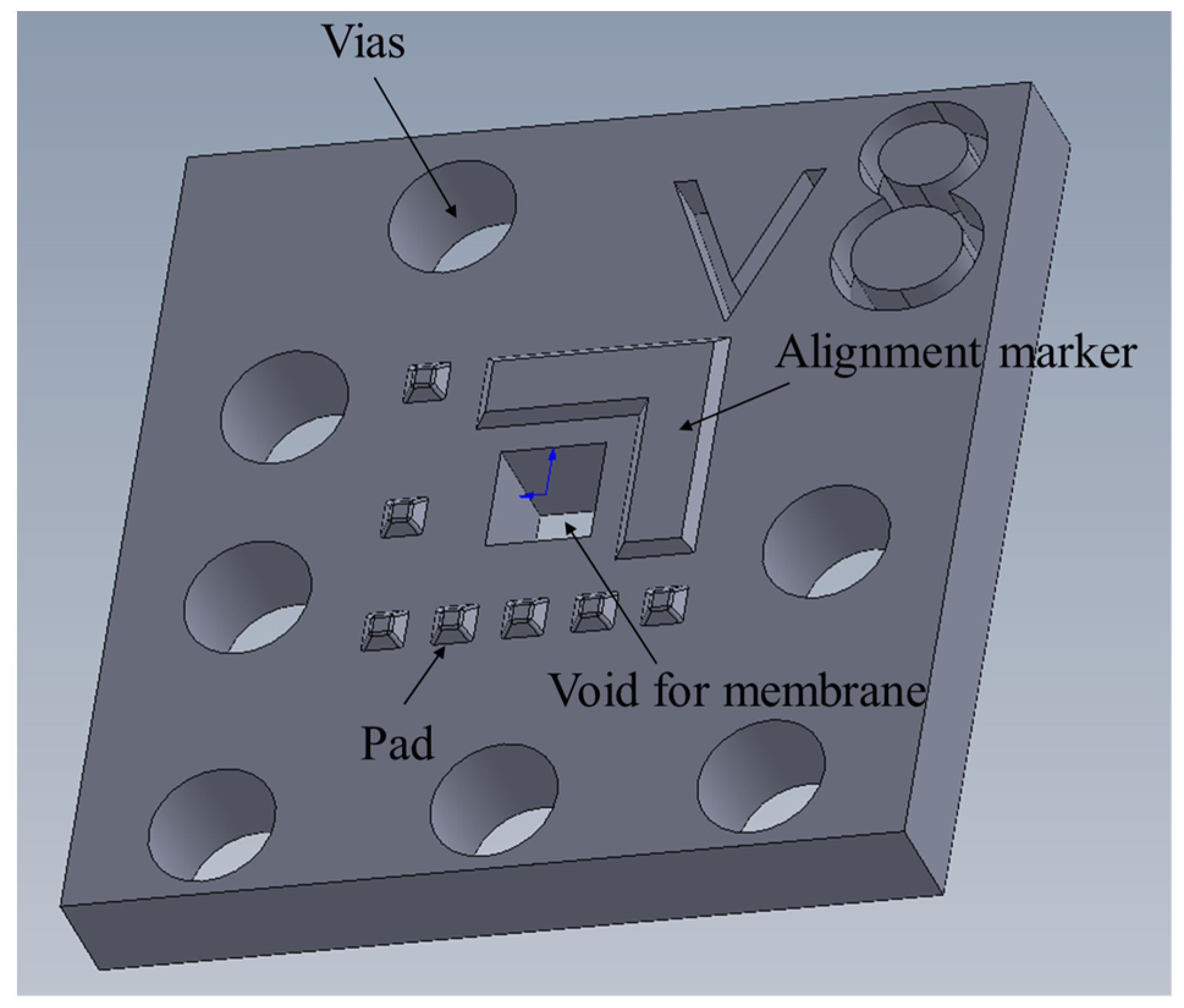
The housing of the package was printed using a high-performance multi-jet 3D printer (ProJet 3510 HDPlus, 3D Systems). The package housing (Figure 1) with dimensions of 8 × 8 × 1 mm, 7 through-holes for electrical vias, central void for gas sensitive membrane and 7 pyramide-like pad structures (150 × 150 µm, 100 µm hight) was printed using a translucent acrylate-type polymer (VisiJet M3 Crystal) in an extreme-high-definition mode with the 750 × 750 × 16,000 dpi resolution. The printing was performed face up and the surface of the print was treated with distilled water and isopropanol.
The vias holes were filled with the silver-filled conductive paste (Polytech PT) using a manual dispensing station (ML-5000 xII, Musashi Engineering, Inc., Tokyo, Japan) and dried/cured at room temperature. The vias-to-pad connections and pads were inkjet printed on the surface of the housing in a single pass using an advanced R&D inkjet printer (PiXDRO LP50, Meyer Burger Technology AG, Thun, Switzerland) equipped with an industrial inkjet print-head (SM-128 Spectra S-class, Fujifilm Dimatix, Inc., Santa Clara, CA, USA) with a 50 µm nozzle dimeter and 50 pL calibrated drop size. The nanoparticle Ag ink (Sycris I50TM-119, PV Nanocell, Migdal Haemek, Israel) with 50 wt. % metal loading and average particle size of 120 nm (d90) was deposited at the carefully adjusted jetting profile.
2.2. Photonic Sintering
The inkjet-printed Ag structures were sintered using a photonic sintering device (PulseForge 1200, Novacentrix, TX, USA). A photonic processing consisting of 4 µ-pulses with overall length of 2800 µs at 250 V with relatively low amount of energy (728 mJ·cm−2) was used for the sintering of the printed structures; the average sheet resistance of around 200 mΩ·sq−1 was measured with the four-point probe technique (C4S, Cascade Microtech GmbH, Beaverton, OR, USA).
2.3. Flip-Chip Fine Placing
The bonding process was carried out by means of a micro-assembly station (FINEPLACER® lambda, Finetech GmbH & Co. KG, Berlin, Germany). As mentioned before, for mounting the chip (C27 absolute pressure sensor dye, TDK) in the 3D-printed housing, a flip-chip approach has been pursued. In this technique, a silver-filled conductive paste (Polytec PT) was firstly dispensed on the housing pads. Thereafter, the chip was flipped over so that its top side faces down, and the chip pads align with the corresponding housing pads. The silver-filled paste, which acts as the interconnector, was then cured for 4 h at room temperature. Throughout the curing process, the electrical resistivity of the conductive paste dropped to 320 mΩ·sq−l. The second approach which was pursued in the current study was to exploit anisotropic conductive pastes (ACP) as an interconnector. Accordingly, a low temperature curable ACP paste (DELO-adhesives) was dispensed in the similar manner and cured at 60 °C. However, a low bonding pressure (4N) was employed during ACP bonding process.
3. Results and Discussion
3.1. 3D Microfabrication
The inkjet-printed Ag contacts and pads are shown in Figure 2a. The integrated alignment system of the printer’s software allowed the exact alignment on the edge of the 3D printed housing; the circular structures were printed on the Ag-filled vias and they were connected to the pad positions, which were 100 µm higher than the overall printed surface. The reason for the different height is the flip-chip connection of the pressure sensor dye in the next step: the sensor dye did not have the standard flip-chip bumps: this was creatively solved with the 3D pads on the package itself. The pads printed on the pyramide-like structures were much larger (400 µm) than the flat surface of the 3D structures (150 µm): the idea was to completely cover the 3D structures with conductive layer to improve the contact between the chip dye and the printed package.
3.2. Chip-to-Package Contact
The sensor dye was placed on the printed package and aligned according to the contact pads on the dye. Two different contacting methods were pursued: the first one exploited only the physical contact between the sensor pad and the printed package pad. In this case, the alignment marker was covered with the UV glue and the dye was aligned, pressed and subsequently UV cured from the side. Although the system itself showed a sufficient physical stability, the electrical connection between the two pads did not suffice. The surface of the UV glue around the chip was enhanced in the second prototype; the electrical connection did not improve most probably due to the insulation of some pads with the UV glue as well as the softness and bendability of the printed substrate.
The second method exploits the unique properties of the anisotropic conductive glue (ACP). While the thermal stability of the package is quite limited (low distortion temperature of the printed polymer, 56 °C), a thorough compatibility study of different low-temperature ACPs with the printed system will be conducted as the next step. The electrical connection measurements and the validation measurements of the pressure sensor package will be performed in a customized pressure sensor chamber with a controlled pressure function.
Acknowledgments
This project has received funding from the Electronic Component Systems for European Leadership Joint Undertaking under grant agreement No. 692480. This Joint Undertaking receives support from the European Union's Horizon 2020 research and innovation programme and Germany, Saxony, Spain, Austria, Belgium, Slovakia. The project IoSense is co-funded by Austrian Research Promotion Agency (FFG).
Conflicts of Interest
The authors declare no conflict of interest.
References
- Vaezi, M.; Seitz, H.; Yang, S. A review on 3D micro-additive manufacturing technologies. Int. J. Adv. Manuf. Technol. 2013, 67, 1721–1754. [Google Scholar] [CrossRef]
- Kim, D.; Lee, S.H.; Jeong, S.; Moon, J. All-Ink-Jet printed flexible organic thin-film transistors on plastic substrates. Electrochem. Solid St. 2009, 12, H195–H197. [Google Scholar] [CrossRef]
- Cook, B.S.; Mariotti, C.; Cooper, J.R.; Revier, D.; Tehrani, B.K.; Aluigi, L.; Roselli, L.; Tentzeris, M.M. Inkjet-printed, vertically-integrated, high-performance inductors and transformers on flexible LCP substrate. IEEE MTT-S Int. Microw. Symp. 2014, 1–4. [Google Scholar] [CrossRef]
- Cook, B.S.; Cooper, J.R.; Tentzeris, M.M. Multi-Layer RF capacitors on flexible substrates utilizing inkjet-printed dielectric polymers. IEEE Microw. Compon. Lett. 2013, 23, 1531–1309. [Google Scholar] [CrossRef]
- Korvnik, J.G.; Smith, P.J.; Shin, D.-Y. Overview of Inkjet-Based Micromanufacturing. In Inkjet-Based Micromanufacturing; Wiley-VCH Verlag GmbH & Co. KGaA: Weinheim, Germany, 2012. [Google Scholar]
- Szendiuch, I. Development in Electronic Packaging—Moving to 3D System Configuration. Radioengineering 2011, 20, 214–220. [Google Scholar]
- Krivec, M.; Roshanghias, A.; Abram, A.; Binder, A. Exploiting the combination of 3D polymer printing and inkjet Ag-nanoparticle printing for advanced packaging. Microelectron. Eng. 2017, 176, 1–5. [Google Scholar] [CrossRef]
Figure 1.
3D sketch of the package housing printed with the multi-jet polymer printer.

Figure 2.
(a) 3D- and inkjet-printed package with conductive paths, pads and through-via contacts (without sensor dye); (b) Optical image of the alignment and fine placing of the pressure sensor dye on the printed package.
Figure 2.
(a) 3D- and inkjet-printed package with conductive paths, pads and through-via contacts (without sensor dye); (b) Optical image of the alignment and fine placing of the pressure sensor dye on the printed package.

Publisher’s Note: MDPI stays neutral with regard to jurisdictional claims in published maps and institutional affiliations. |
© 2017 by the authors. Licensee MDPI, Basel, Switzerland. This article is an open access article distributed under the terms and conditions of the Creative Commons Attribution (CC BY) license (https://creativecommons.org/licenses/by/4.0/).
Share and Cite
MDPI and ACS Style
Krivec, M.; Roshanghias, A.; Binder, A. 3DInkPack—Inkjet Printing of Discrete Sensor Packages for Advanced Rapid Prototyping. Proceedings 2017, 1, 609. https://doi.org/10.3390/proceedings1040609
AMA Style
Krivec M, Roshanghias A, Binder A. 3DInkPack—Inkjet Printing of Discrete Sensor Packages for Advanced Rapid Prototyping. Proceedings. 2017; 1(4):609. https://doi.org/10.3390/proceedings1040609
Chicago/Turabian StyleKrivec, Matic, Ali Roshanghias, and Alfred Binder. 2017. "3DInkPack—Inkjet Printing of Discrete Sensor Packages for Advanced Rapid Prototyping" Proceedings 1, no. 4: 609. https://doi.org/10.3390/proceedings1040609