Fabrication of Planar Copper Microcoils for Telemetric Orthodontic Applications †
by
Julian Hafner
1, 
Matthias Kuhl
2,
Michael Schwaerzle
1,
Thorsten Hehn
3,
Daniel Rossbach
3 and
Oliver Paul
1,* 1
Laboratory for Microsystem Materials, Departement of Microsystems Engineering (IMTEK) & Cluster of Excellence Brainlinks-Brain-Tools, University of Freiburg, D-79110 Freiburg, Germany
2
Fritz-Huettinger-Chair for Microelectronics, Departement of Microsystems Engineering (IMTEK) & Cluster of Excellence Brainlinks-Brain-Tools, University of Freiburg, D-79110 Freiburg, Germany
3
Hahn-Schickard, Wilhelm-Schickard-Str. 10, 78052 Villingen-Schwenningen, Germany
*
Author to whom correspondence should be addressed.
†
Presented at the Eurosensors 2017 Conference, Paris, France, 3–6 September 2017.
Proceedings 2017, 1(4), 571; https://doi.org/10.3390/proceedings1040571
Published: 9 August 2017
(This article belongs to the Proceedings of Proceedings of Eurosensors 2017, Paris, France, 3–6 September 2017)
Abstract
:The fabrication of electroplated planar copper microcoils for telemetric orthodontic applications is presented. A set of microcoils with overall dimensions of 2 × 2.5 × 0.5 mm3, track widths down to 5 μm and turn numbers up to 35 were fabricated on glass substrates. The coils were electrically characterized and assembled via flip-chip bonding onto a stress-mapping CMOS chip for smart orthodontic brackets. The passive system was successfully read out telemetrically with a reader microcoil for a coil-coil distance of 1 mm at 13.56 MHz. The digital signal representing the measured stress values was extracted telemetrically using a commercially available RFID reader.
1. Introduction
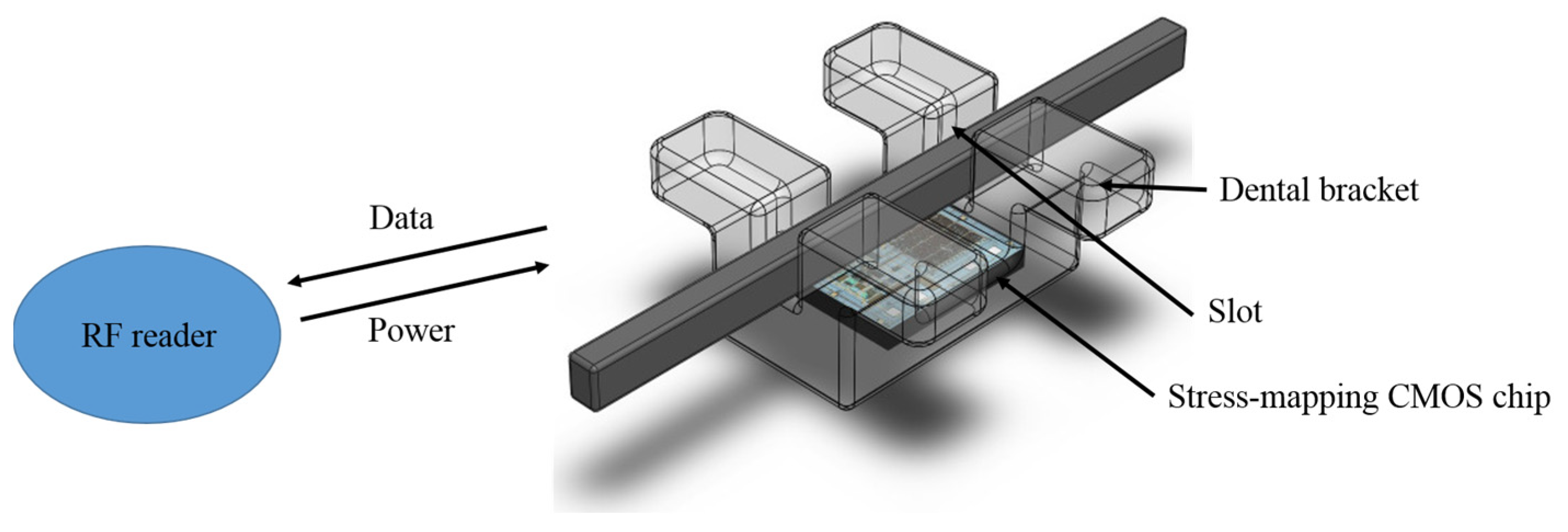
In orthodontics, the forces and moments applied to the teeth are of utmost importance for the duration and effectiveness of the therapy. Excessive loads lead to irreparable root damage, while subcritical forces unnecessarily extend therapy duration. For in situ force and moment measurements, a stress-mapping CMOS chip has been proposed [1]. It includes several piezoresistive stress sensors and an RF interface. It is designed to be implanted between bracket base and slot as illustrated in Figure 1. The telemetric link can be realized inductively with a hybridly integrated planar microcoil.
Microfabrication of planar microcoils using electroplated Cu has been heavily discussed in the past [3,4]. Fabrication approaches based on a uniform seed layer for coil electroplating have revealed a number of problems during wet seed layer removal after electroplating: Structural delamination and seed layer residues between adjacent coil lines, among others. These issues become particularly critical at line and space dimensions below 10 μm and aspect ratios larger than 2. Structured seed layers as proposed in [3] potentially solve this problem, but most likely result in inhomogeneous plating of high-density structures due to inhomogeneous plating potential. Seed layer removal by ion-beam etching as proposed in [4] is usually avoided in the case of Cu substrates, due to the increased risk of cross-contamination during semiconductor manufacturing. This work presents an approach in which these challenges are addressed using an additional process step. The accordingly processed coils were electrically characterized and assembled onto a stress-mapping CMOS chip via flip-chip bonding. Finally, the telemetric link was tested and the digital sensor information was extracted telemetrically.
2. Microcoil Fabrication
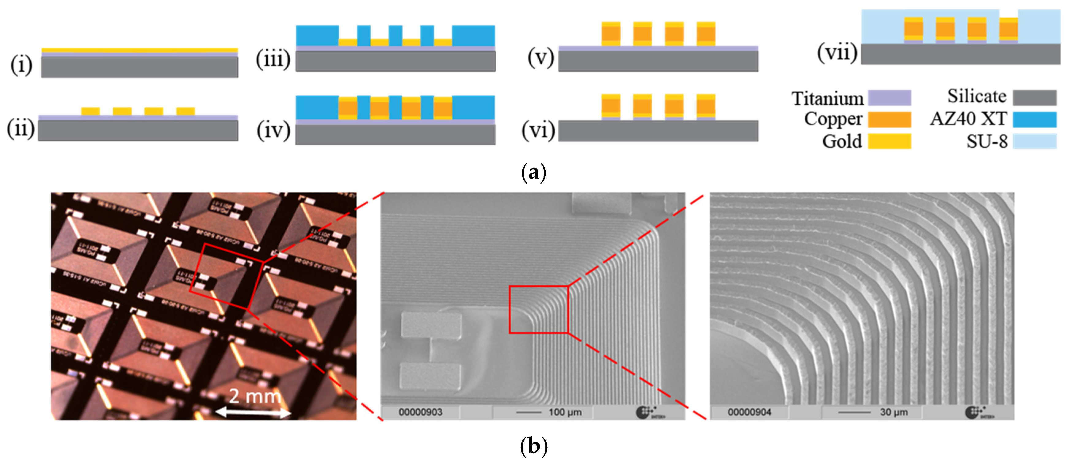
The process sequence for microcoil fabrication on silicate-glass substrates is illustrated in Figure 2a. It starts by sputtering a seed layer metallization {50 nm titanium (Ti), 100 nm gold (Au)} onto 300 to 500-μm-thick glass substrates. This is followed by a first photolithography step applying a thin-film resist as a masking layer for the subsequent dry etching. The Au layer is then structured by ion beam etching while the Ti layer is left intact. The result is a half-structured metal layer, where Ti serves as a conductive path and Au as a seed layer for electroplating. Au was found to show reliable plating adhesion to the electroplated Cu structures whereas Ti is preferred due to its capability of being wet-etched selectively against Cu. After the second photolithography step using the 30-μm-thick resist AZ40XT, Cu is electroplated up to a height of about 22 μm. In addition, a 2–3 μm thick layer of Au is electroplated to improve bonding adhesion to the coil top surface. The resist is stripped and the exposed Ti is etched selectively using a 1% hydrofluoric acid solution in combination with the non-ionic surfactant Triton X-100 agitated in a megasonic bath. This results in free-standing copper microcoils as illustrated in Figure 2b. Encapsulation is performed by spin coating a 50-μm-thick SU-8 resist followed by a photolithographic opening of the contact pads. After encapsulation, the diced microcoils can be contacted via wire or flip-chip bonding.
3. Electrical Characterization
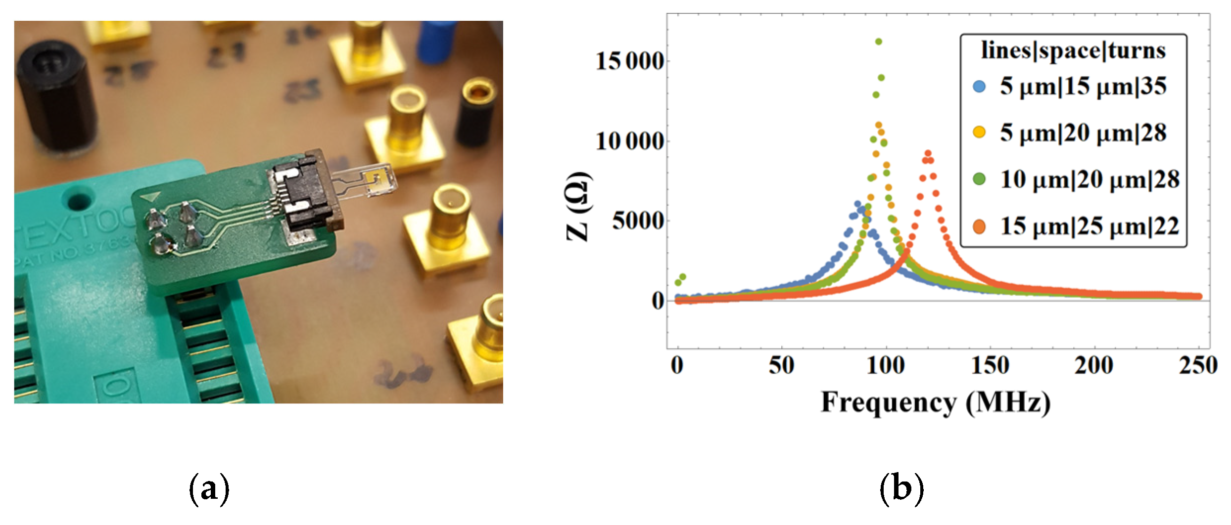
For electrical characterization, the microcoils were connected to a glass rewiring chip by flip-chip bonding. Furthermore, the measurement setup comprises a ZIF connector for the insertion of different microcoils and the network analyzer Agilent 4395A (Keysight Technologies, 71034 Böblingen, Germany). After calibration, the impedance curves were measured and the inductance, (parasitic) capacitance and DC resistance were extracted applying a simple RLC model. The impedance curves were measured for a set of four different microcoils with 22–35 windings, track widths of 5–15 μm and track spaces of 15–25 μm. The measured curves are illustrated in Figure 3b). The extracted inductance values were then compared to numerical simulation results obtained with the freeware tool Fastfieldsolvers (FastFieldSolvers S.R.L, 20871 Vimercate (MB), Italy) [5]. The results are illustrated in Table 1. In summary, the microcoils show inductance values of 1.4–2 μH, parasitic capacitances of about 2 pF, DC resistances of 7–30 Ω and self-resonance frequencies of 80–120 MHz. The coil with the highest inductance of about 2 μH was identified to be the most promising candidate for the system assembly with the stress-mapping CMOS chip in view of its resonant operation at 13.56 MHz.
4. System Assembly and Telemetric Link
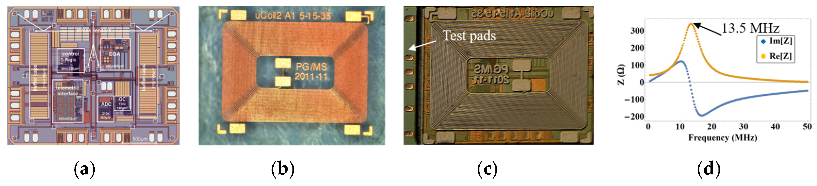
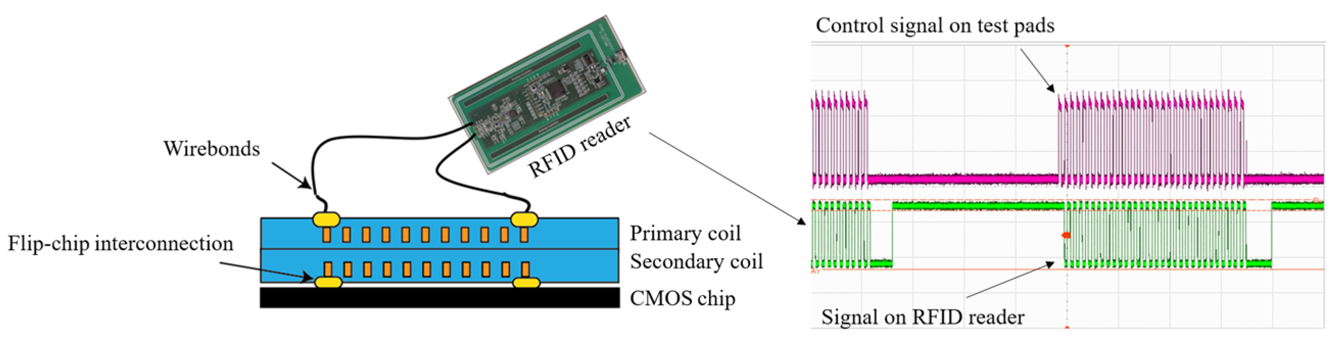
The assembly of the microcoil with the stress-mapping CMOS chip is illustrated in Figure 4. The interconnection was performed by flip-chip bonding. By connecting the indicated test pads using wire-bonding the input impedance of the assembly was measured. The measured impedance curve is illustrated in Figure 4d. The system resonates near the target frequency of 13.56 MHz. The test pads also provide the opportunity to test the functionality of the stress-mapping CMOS chip.
A second microcoil serving as the reader antenna was attached adhesively to the assembly. This reader coil was then connected to the RFID Reader ST25R3911B-DISCO (STMicroelectronics, Geneva, Switzerland) which was controlled via a graphical user interface. The reader is equipped with an automatic tuning feature which tunes the antenna to resonate at 13.56 MHz. The RFID reader can be set to the so-called transparent mode, which allows to read out the raw digital signals. The data packages containing the digital sensor information were extracted at the pins of the RFID reader. The measured digital signal is illustrated in Figure 5.
5. Conclusions
In this paper, we presented a fabrication and assembly approach for planar copper microcoils together with a telemetric microsystem assembly consisting of a stress-mapping CMOS chip and a microcoil. It was shown that the coil design meets the requirements of the assembly to resonate near 13.56 MHz. The digital sensor data were extracted telemetrically using a second microcoil acting as a reader antenna. The assembly of the telemetric device in Figure 4 represents a dramatically miniaturized passive RFID tag with dimensions of only 2 × 2.5 × 0.8 mm3 with an integrated stress sensor system. It paves the way to the telemetric extraction of stress sensor data in highly compact application scenarios such as orthodontics.
Acknowledgments
The research leading to these results has received funding from the BrainLinks-BrainTools Cluster of Excellence (grant number EXC 1086) and projects MA 2193/7-1 & PA 792/5-1, all funded by the German Research Foundation DFG. The authors gratefully acknowledge technical support by Michael Reichel and Armin Baur (both IMTEK-RSC) during cleanroom fabrication.
Conflicts of Interest
The authors declare no conflict of interest. The founding sponsors had no role in the design of the study; in the collection, analyses, or interpretation of data; in the writing of the manuscript, and in the decision to publish the results.
References
- Kuhl, M.; Gieschke, P.; Rossbach, D. A telemetric stress-mapping CMOS chip with 24 FET-based stress sensors for smart orthodontic brackets. In Proceedings of the 2011 IEEE International Solid-State Circuits Conference Digest of Technical Papers (ISSCC), San Francisco, CA, USA, 20–24 February 2011; pp. 108–110. [Google Scholar]
- Bartholomeyczik, J. Advanced CMOS-Based Stress Sensing. Ph.D. Thesis, Department of Microsystems Engineering (IMTEK), University of Freiburg, Freiburg im Breisgau, Germany, 30 April 2006. [Google Scholar]
- Moulin, J.; Woytasik, M.; Martincic, E.; Dufour-Gergam, E. Copper planar microcoils applied to magnetic actuation. In Proceedings of the DTIP; HAL: Stresa, Lago Maggiore, Italy, 2007; hal-00257693; pp. 225–229. [Google Scholar]
- Neagu, C.R.; Jansen, H.V.; Smith, A.; Gardeniers, J.G.E.; Elwenspoek, M.C. Characterization of a planar microcoil for implantable microsystems. Sens. Actuators A Phys. 1997, 62, 599–611. [Google Scholar] [CrossRef]
- Fastfieldsolvers. Available online: http://www.fastfieldsolvers.com (accessed on 28 June 2017).
Figure 1.
Dental bracket with stress-mapping CMOS chip for telemetric stress measurement during orthodontic therapy (adapted from [2]).
Figure 1.
Dental bracket with stress-mapping CMOS chip for telemetric stress measurement during orthodontic therapy (adapted from [2]).

Figure 2.
(a) Microcoil fabrication sequence; (i) Seed layer sputter deposition; (ii) Ion beam etching; (iii) 30 μm AZ40XT photolithography; (iv) Cu + Au electroplating; (v) Resist strip in megasonic bath; (vi) Wet selective seed layer etching; (vii) SU-8 encapsulation; (b) 22-μm-high free-standing microcoils with 5 μm linewidth and 15 μm spacing after etching. Vertical layer dimensions in (a) are not to scale.

Figure 3.
(a) Measurement setup for electrical microcoil characterization; (b) Real part of impedance curves measured for four different microcoils.
Figure 3.
(a) Measurement setup for electrical microcoil characterization; (b) Real part of impedance curves measured for four different microcoils.

Figure 4.
(a) Stress-mapping CMOS chip; (b) Microcoil with 35 windings; (c) Flip-chip assembly; (d) Measured assembly input impedance (real and imaginary parts) with resonance peak near 13.56 MHz.
Figure 4.
(a) Stress-mapping CMOS chip; (b) Microcoil with 35 windings; (c) Flip-chip assembly; (d) Measured assembly input impedance (real and imaginary parts) with resonance peak near 13.56 MHz.

Figure 5.
Schematic of telemetric readout setup with microcoil acting as primary coil (reader antenna), RFID reader and telemetrically extracted digitized signal representing the sensor data.
Figure 5.
Schematic of telemetric readout setup with microcoil acting as primary coil (reader antenna), RFID reader and telemetrically extracted digitized signal representing the sensor data.


Table 1.
Extracted electrical characteristics of four different microcoils compared to simulation.
| Lines | Space | Turns | Measurement | Simulation |
|---|---|---|
| 5 μm | 15 μm | 35 | 2.09 μH | 30 Ω | 1.9 pF | 3.3 μH | 38 Ω | 0.29 pF |
| 5 μm | 20 μm | 28 | 1.58 μH | 23 Ω | 1.9 pF | 2.0 μH | 30 Ω | 0.29 pF |
| 10 μm | 20 μm | 28 | 1.42 μH | 14 Ω | 1.6 pF | 2.0 μH | 15 Ω | 0.29 pF |
| 15 μm | 25 μm | 22 | 1.03 μH | 7 Ω | 1.7 pF | 1.3 μH | 8 Ω | 0.29 pF |
Publisher’s Note: MDPI stays neutral with regard to jurisdictional claims in published maps and institutional affiliations. |
© 2017 by the authors. Licensee MDPI, Basel, Switzerland. This article is an open access article distributed under the terms and conditions of the Creative Commons Attribution (CC BY) license (https://creativecommons.org/licenses/by/4.0/).
Share and Cite
MDPI and ACS Style
Hafner, J.; Kuhl, M.; Schwaerzle, M.; Hehn, T.; Rossbach, D.; Paul, O. Fabrication of Planar Copper Microcoils for Telemetric Orthodontic Applications. Proceedings 2017, 1, 571. https://doi.org/10.3390/proceedings1040571
AMA Style
Hafner J, Kuhl M, Schwaerzle M, Hehn T, Rossbach D, Paul O. Fabrication of Planar Copper Microcoils for Telemetric Orthodontic Applications. Proceedings. 2017; 1(4):571. https://doi.org/10.3390/proceedings1040571
Chicago/Turabian StyleHafner, Julian, Matthias Kuhl, Michael Schwaerzle, Thorsten Hehn, Daniel Rossbach, and Oliver Paul. 2017. "Fabrication of Planar Copper Microcoils for Telemetric Orthodontic Applications" Proceedings 1, no. 4: 571. https://doi.org/10.3390/proceedings1040571