A Tunable Multi-Port Fano Resonator Based on Mach-Zehnder Interferometers Coupling with Micro-Ring Resonators
by
 , and
, and
Yingjie Xu
1 ,
,
Lidan Lu
1,*,
Guang Chen
1,
Jie Liao
1,
Xiaofeng Xu
1,
Jianzhen Ou
2 and
Lianqing Zhu
1,* 1
School of Instrument Science and Opto-Electronics Engineering, Beijing Information Science and Technology University, Beijing 100029, China
2
School of Engineering, RMIT University, Melbourne 3000, Australia
*
Authors to whom correspondence should be addressed.
Photonics 2022, 9(10), 725; https://doi.org/10.3390/photonics9100725
Submission received: 17 August 2022
/
Revised: 28 September 2022
/
Accepted: 1 October 2022
/
Published: 5 October 2022
Abstract
:Fano resonance has an asymmetric and sharp resonance peak near the resonance wavelength, which can effectively enhance the all-optical signal processing capability and realize silicon photonic switches, sensors, and modulators. In this paper, a silicon photonic Fano resonator with Mach-Zehnder interferometer (MZI) structure coupling with micro-ring resonators (MRR) is designed. Two MRRs with different quality factors are coupled with two arms of an MZI, and the coupling zone is composed of two half-ring waveguides. Based on the transfer matrix method, the intrinsic and modulated transfer characteristics of the component are analyzed. By adjusting the optical amplitude and phase of MZIs and tuning the resonance wavelength of two MRRs, Fano resonance spectra are simulated at four output ports with the highest extinction ratios of 56.19 dB and maximum slope rates at 2175.74 dB/nm, and the transmission spectra of Fano resonance at the four output ports are experimentally demonstrated. As the four Fano resonance ports of the designed component have different performances, they can be used for various functions simultaneously. The advantage of the proposed scheme is the improvement of the multiplexing capacity and simultaneous utilization of the muti-port for the Fano resonator. Our four-port Fano resonator can be employed in the fields of optical switching, optical computing, and optical interconnect in the future.
1. Introduction
Fano resonance is generated by the mutual coupling of discrete and continuous states, and its spectrum shows sharp asymmetric lines. Fano resonance can effectively enhance the ability of all-optical signal processing. Moreover, it has been applied to high-sensitivity sensing [1], optical switches [2], and silicon modulators [3]. The high integration of silicon photonic components and their compatibility with Complementary Metal Oxide Semiconductor (CMOS) techniques have prompted them replacing traditional optical components. Silicon photonic crystal nanobeam cavities (PCNC) [4,5], micro-ring resonators (MRRs) [6,7], and Mach-Zehnder interferometers (MZIs) [8,9,10] have been reported to achieve Fano resonance. Herein, the PCNC structure [11] has a strong confinement effect on photonics, so the discrete light mode is laterally coupled with the continuous mode, quasi-continuous mode, and photonic crystal bandgap edge mode [12]. Thus, Fano resonance can be obtained by PCNC. However, the photon lifetime of PCNC is low [13] due to its periodic holes. The extinction ratio (ER) and slope rate (SR) are two essential parameters to characterize the transmission spectrum of Fano resonance. ER refers to the light intensity difference between the valley and peak of the Fano spectrum, and SR (also called spectral resolution) refers to the change rate of the light intensity with respect to the wavelength between the valley and peak of the Fano resonance. Generally, Fano resonance with high ER and SR is effectively helpful for improving the component performance, such as the response rate and sensitivity for the optical switcher, silicon modulator, optical sensor, and so on. In addition, the machining process of PCNC is comparatively challenged, and the slope rate (SR) and extinction ratio (ER) of the Fano spectra are also low—the ER of the reported Fano resonance produced by PCNC is around 20 dB [4,14,15]. However, as a silicon photonic classical structure, MRR has a high photon lifetime and compact structure. The resonance mode of this MRR structure is usually regarded as the discrete mode so that this discrete mode coupled with continuum/quasi-continuous modes of other silicon waveguide structures can achieve various Fano resonances [8].
Many scholars have studied the single-port output Fano resonator. A single-port Fano resonator composed of a silicon add-drop micro-ring with two integrated tunable reflectors inside has been demonstrated, forming an embedded Fabry-Perot cavity, which can achieve a Fano resonance with a maximum ER of 40 dB and a slope rate of 700 dB/nm [16]. In addition, a Fano-like resonator with a high SR is proposed, whose scheme is based on a symmetrical 2 × 2 multimode interferometer (MMI), and two parallel micro-ring resonators (MRRs) are sandwiched between the two branches of the MMI. The SR of the scheme can vary from −115.04 dB/nm to −247.54 dB/nm [17]. Additionally, a single-port Fano resonator with the highest ER at 56.8 dB and SR at 3388.1 dB/nm based on the silicon waveguide is also achieved [18]. Although the Fano resonator with a single-port output has been investigated widely and deeply [16,17,18,19,20,21], the multiplexing capacity and output signal varieties are always the drawback factors that limit the performance of Fano resonators. Because there is only one output port for Fano resonance, it cannot be applied to scenarios where multi-ports are required. In order to solve this bottleneck issue, a four-output port Fano resonator based on a coupling structure of dual-MRR and MZIs is proposed in this paper, which considerably improves the signal multiplexing capability and realizes the multi-functional integration of the component. Moreover, a multi-port signal output of Fano resonance with a high-performance lineshape is obtained.
This paper is organized as follows. In Section 2, a photonic integrated circuit with a structure of dual-MRR coupling with MZIs is designed and explained by the transmission matrix method (TMM). Furthermore, a simulation model of the Fano resonator based on the silicon waveguide is built and analyzed in Section 3. By adjusting the controlling voltages of MRRs and MZIs, the optimized ER and SR of transmission spectra at the four output ports of the Fano resonator are obtained. In addition, Section 4 shows the fabricated passive silicon component whose features are measured and tested, and the Fano resonance at the four output ports of the component is experimentally verified. In the last section, the characteristics, advantages, and potential applications for our Fano resonator are summarized.
2. Photonic Integrated Circuit Design
These parameters are determined by the coupled-mode theory (CMT) and the transfer matrix method (TMM). The component structure is shown in Figure 1, and the structure is composed of two MRR-coupled MZIs. The green dashed area of the component is MZI1. MZI1 is composed of two multimode interferometers (MMI) and two arms. The optical signal is from a continuous wave laser coupled with the chip via a grating coupler (GC0) and split into the two arms of MZI1 by a multi-mode interferometer (MMI1). After a direct bias voltage V1 is applied to the upper arm of the MZI1, the phase of the optical signal in MZI1′s upper arm and the amplitude of the combined optical signal can be adjusted. Later, the optical signals from the upper and lower arms of MZI1 are combined in MMI2 and are then divided again into two signals that separately enter the two arms of MZI2 The orange dashed area of the component is akin to MZI2. MZI2 comprises two couplers, two arms in the middle, and two MRRs. The low Q-factor MRR is used as a continuous mode. The high Q-factor MRR is used as a discrete mode. The two arms of MZI2 have a high Q-factor (MRR1) and low Q-factor (MRR2) resonator. The discrete state for MRR1 and continuous state for MRR2 light are coupled in the coupling region, and the Fano resonance can be obtained at the four ports from GC1 to GC4. The coupling region is composed of two half-rings. MRR1 with a high Q-factor and MRR2 with a low Q-factor are embedded in the two arms of MZI2, respectively, and their resonance wavelengths are modulated by tuning the direct bias voltages V3 and V4, respectively. The direct bias voltage V2 in MZI2 can tune the coupling phase difference coupled in the two MRRs.
The component can realize a four-port output tunable Fano resonance with a high ER and SR. Fano resonance is achieved by coupling two resonances generated by the MRRs of two different coupling gaps. The component can achieve the function, which involves simultaneously tuning the optical amplitude, phase, ER, SR, and resonance wavelength. By appropriately tuning the direct bias voltages V1 and V2, the amplitude and phase of the optical signal can be changed. The direct bias voltages V3 and V4 tuned the resonance wavelengths of MRR1 and MRR2, respectively. By adjusting the electric power, a Fano resonance with a high ER and SR can be achieved at the output, and the resonance wavelength can also be tuned.
As for the transfer matrix method (TMM), the complex component structure can be disassembled into basic silicon photonic components, and each fundamental component has its unique transmission matrix. We adopt TMM to analyze the designed structure.
The transmission function of the component via the output of GC1 and GC4 can be expressed as:
The transmission function of the component via the output of GC2 and GC3 can be expressed as:
where and are phase shifts adjusted by V1 and V2, respectively. and are amplitude responses of MRR1 and MRR2, respectively. Each matrix represents the corresponding components, which are illustrated in Figure 2. At the right end of Equation (1), represents the two optical signals from the output port of MMI1. Next, represents the phase shifts of MZI1 adjusted by V1. Then, represents the transmission matrix of MMI2, and represents the transmission matrix of the MRR1 and MRR2. At the left end, represents the transmission matrix of the coupling region in MRR1 and MRR2. Similarly, the only difference in Equation (2) is that there is an added matrix , which represents another coupling region between the ring waveguide and bus waveguide. This method’s theoretical derivation provides a basis for subsequent photonic integrated circuit simulation.
3. Simulation Results and Analysis
In the simulation model of the component, the results have an optimal performance when the following structural parameters are selected. The length of both arms of MZI1 is 325 μm, and the radiuses of two MMRs are both selected as 40 μm. The coupling gaps of MRR1 and MRR2 are 0.3 μm and 0.2 μm, respectively. The coupling coefficient of MMR1 is 0.155508, and the coupling coefficient of MMR2 is 0.321836. In the coupling region between MRR1 and MRR2, the radius of the half-ring for the MZI2 is 80 μm. The input signal is from a continuous wave laser with broadband from 1500 nm to 1600 nm in the simulation.
Herein, a simulation tool that can design, simulate, and analyze integrated optical circuits, silicon photonic components, and optical interconnect systems is utilized. Based on the transfer matrix method via system-level simulation for the photonic integrated circuit, it can effectively guide us in designing silicon photonic components. These papers [22,23] show that the simulation results from Lumerical INTERCONNECT are consistent with the experimental results. Thus, we use this tool for simulation verification. The modulation of the component can be achieved by both the thermo-optic effect [24] and carrier dispersion effect [25]. Therefore, these two effects can be used to adjust the refractive index by changing the voltages. The plasma dispersion effect can cause a greater change in the refractive index than the thermo-optical effect. Thus, the carrier dispersion effect is used to change the refractive index in this paper. The change in the refractive index through different voltages is shown in Figure 3.
As seen from Figure 4a to Figure 4d, all four ports (from GC1 to GC4) can output corresponding Fano resonance spectra, and the spectral performances of the Fano resonance output from the four ports are different. Since the performance of each port is different, the optimal ER and SR of each port are at different wavelength ranges. The port at GC1 can output a high ER for Fano resonance, and the ports at GC2 and GC3 can output high SR for Fano resonance. The ER and SR of each port are different, and we can choose the port according to the needs. At the GC1 port, the ER and SR are 23.73 dB and 65.09 dB/nm. At the GC2 port, the ER and SR are 19.49 dB and 974.39 dB/nm. At the GC3 port, the ER and SR are 15.71 dB and 1989.86 dB/nm. At the GC4 port, the ER and SR are 16.48 dB and 55.33 dB/nm.
The free spectral range (FSR) is an important performance parameter for the signal multiplexing capability. The FSRs of different Q-factors for MRR1,2 are shown in Table 1. When the Q-factors of MRR1,2 are determined, the FSRs of the four ports are fixed as the same value. Herein, for simplification, only the FSRs of the GC3 port are illustrated in Figure 5. Obviously, the higher the Q-factor is, the lower the FSR is. Therefore, the FSR can be adjusted by changing the Q-factor. The Q-factor is mainly related to the radius of the MRR and to the coupling gap between the ring waveguide and the bus waveguide.
The optical amplitude can be adjusted by V1 on one arm of MZI1. After the voltage is applied, the effective refractive index of the waveguide is changed. Then, the phase difference has occurred in the two arms of MZI1, and it is converted into light intensity changes through the action of the Multimode interferometer (MMI), thereby completing the optical intensity modulation. The four-port output of GC1, GC2, GC3, and GC4 is shown by applying different voltages of V1 in Figure 6. The optimal spectrum for each port is at a different wavelength. Thus, depending on the application wavelength, we can apply the four ports to different places.
ER and SR of four ports are shown from Figure 7a to Figure 7d, respectively, with different V1. At the GC1, the ER can tune from 23.73 dB to 54.86 dB, and the SR can tune from 65.09 dB/nm to 182.85 dB/nm. At the GC2, the ER can tune from 18.40 dB to 32.92 dB, and the SR can tune from 919.94 dB/nm to 1172.36 dB/nm. At the GC3, the ER can tune from 14.71 dB to 47.08 dB, and the SR can tune from −941.62 dB/nm to 2037.95 dB/nm. The switch between positive SR and negative SR can be realized at the GC3 port. At the GC4, the ER can tune from 17.98 dB to 20.06 dB, and the SR can tune from 57.89 dB/nm to 64.72 dB/nm. The four ports have different performances. Moreover, each port has a different spectral performance after applying voltage.
After adjusting V1 to output the optimal ER and SR state, it can adjust V2. V2 tuned the phase difference between the high Q-factor MRR and the low Q-factor MRR. The phase cannot be observed in the spectrum. However, the phase that is adjusted can also change the light intensity amplitude. Thus, the transmission spectra resulting from adjusting V2 are shown in Figure 8. Therefore, the spectrum can also be optimized by adjusting V2 to obtain a higher ER and SR. The highest ER of the GC1 port is 56.19 dB, and the highest SR of the GC1 port is 184.27 dB/nm. The highest ER of the GC2 port is 32.92 dB, and the highest SR of the GC2 port is 2175.74 dB/nm. The highest ER of the GC3 port is 16.61 dB, and the highest SR of the GC3 port is 2102.39 dB/nm. The highest ER of the GC4 port is 18.37 dB, and the highest SR of the GC4 port is 64.72 dB/nm.
After adjusting V1 and V2 to obtain the optimal ER and SR, we adjust V3. V3 tuned the Fano resonance wavelength. Output transmission spectra with different V3 are shown in Figure 9. Since the four ports have different performances, we apply different voltages. The resonance wavelength is blue-shifted after the V3 voltage is applied. We can observe that the higher the voltage is applied, the more the wavelength shifts, because the effective refractive index decreases.
After adjusting V1, V2, and V3, V4 is adjusted. The function of regulating V4 is similar to that of regulating V3. V4 tuned the Fano resonance wavelength. The transmission spectra with different V4 are shown in Figure 10. The observed results are similar to those of different V3. We can observe that the higher the voltage is applied, the more the wavelength shifts.
4. Experimental Results
We fabricate the designed silicon photonics component to verify the above theoretical simulation. Figure 11 displays its optical microscope image. The waveguide is a silicon-on-insulator (SOI), whose top silicon layer has a thickness of 220 nm and a width of 0.45 μm, and whose buried dioxide layer (silica) has a thickness of 2 μm. The total size of this component is 780 um × 520 um. The fabricated size was consistent with the above simulation size. Electron beam lithography and inductively coupled plasma etching are employed to define the components. The grating is zoomed in on in the scanning electron microscope (SEM) image shown in Figure 11a. The coupling region of the MRR is zoomed in on in the SEM image shown in Figure 11b.
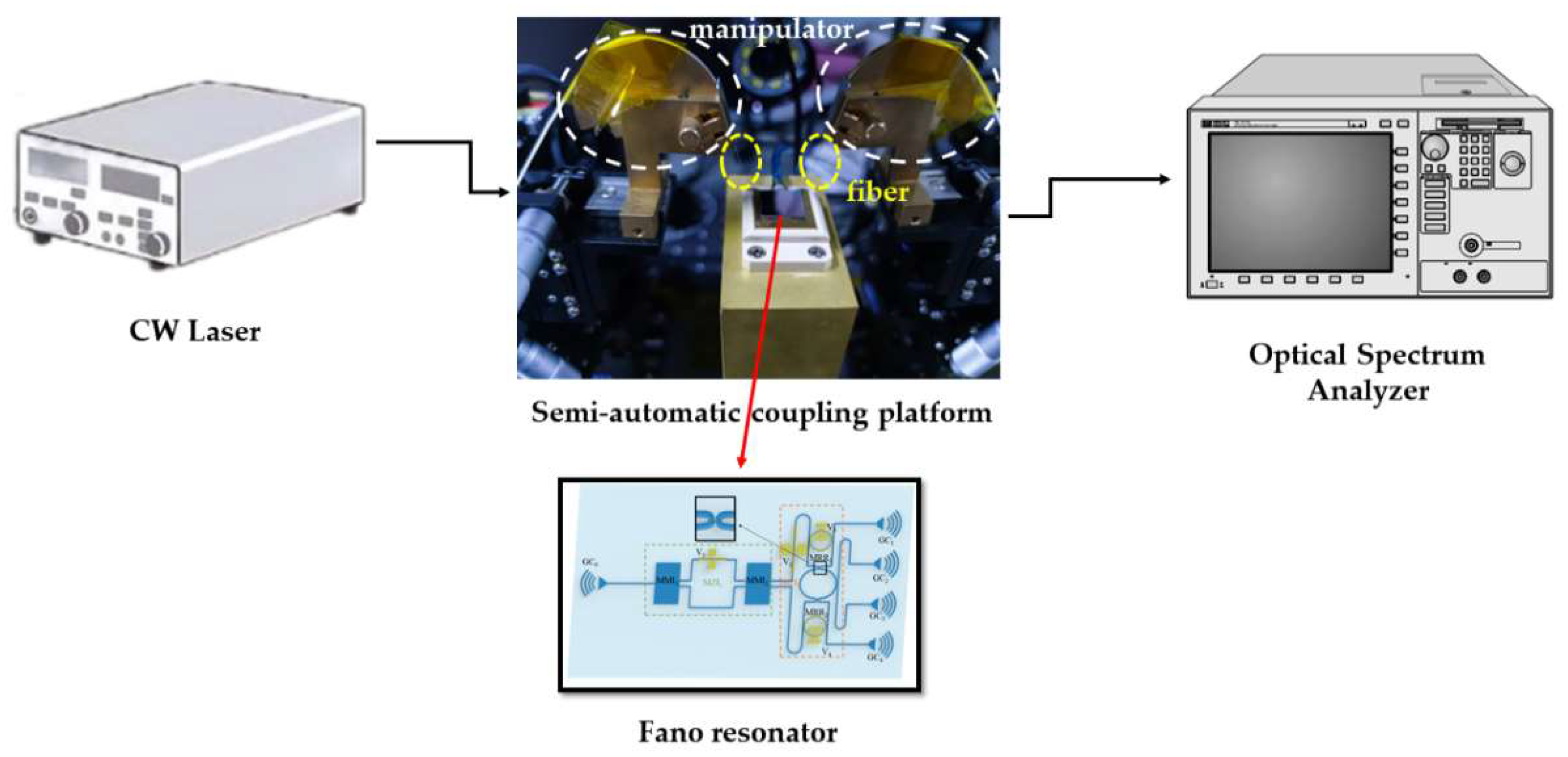
The measurement system of the component is shown in Figure 12. The measurement setup is the optical source, semi-automatic coupling platform, and optical spectrum analyzer (OSA). The optical source is a continuous wave (CW) laser with a broadband from 1500 nm to 1600 nm, where the loss is comparatively low. The light from the CW laser is coupled to the component at the GC0 port through the optical fiber, and the spectra at the four output ports (GC1-GC4) are observed in the OSA. The component is placed on a semi-automatic coupling platform, and the optical fiber is aligned with the grating coupler of the component by the manipulator. The wavelength of the grating coupler also ranges from 1500 nm to 1600 nm, where the loss is comparatively low. In addition, the incident angle between the grating coupler and fiber is around 10°.
As seen in Figure 13, all four ports (GC1, GC2, GC3, GC4) can output Fano resonance spectra in the experiment. At the GC1 port, the ER and SR are 3.60 dB and 9.47 dB/nm. At the GC2 port, the ER and SR are 15.10 dB and 23.59 dB/nm. At the GC3 port, the ER and SR are 16.60 dB and 29.64 dB/nm. At the GC4 port, the ER and SR are 6.85 dB and 21.41 dB/nm. The experiments show that all four ports of this component can output Fano resonance. The measured ER and SR are optimized in the optimal band for each port. If some averaging method is used, the ER and SR will be degraded. Although the feasibility of this component has been experimentally verified, there are some degradations of ER and SR compared with simulation results due to manufacturing and fabrication deviation.
The comparison of the transmission spectra between the simulation and experiment is shown in Figure 14. The positions of the resonance peaks for ports GC1 and GC4 are approximative between the simulation and experiment, but there are obvious differences in ER and SR. At GC2 and GC3, the position of the resonance peaks is also similar along the wavelength between the simulation and experiment. However, the wavelength of the resonance peak is slightly shifted in the experiment compared with the simulation, and the ER and SR of the experiment are also lower than those of the simulation. Moreover, the fabrication process procedures include photoresist-coating, photoresist-baking, electron beam exposure, development, etching, and photoresist-removing. We can hardly obtain high-performance components when not all the processing parameters of these procedures are precisely controlled. In addition, the limitation of our fabrication equipment is that the accuracy of the alignment of the writing field for the electron beam lithography system (EBL) is not high enough. Based on the above reasons, the components have some fabrication mismatches, such as the waveguide length, waveguide width, coupling gap, etching depth of coupling gratings, and so on. Although there are some mismatches between the simulation and experimental results, the functions of the component—improved multiplexing capacity and simultaneous utilization of multi-port for Fano resonator—have also been realized to a certain extent.
5. Conclusions
In this paper, a four-output port Fano resonator with a MZI structure coupling with silicon waveguide MRRs is designed and fabricated. This four-port Fano resonator can be tuned by adjusting the bias voltages of MZIs and MRRs, and the maximum ER and SR of the component are 56.19 dB and 2175.74 dB/nm, respectively. Our demonstrated multi-port Fano resonator has various advantages, such as a higher parallelizability, lower power consumption, higher integration, and versatility. Therefore, it can be employed in the fields of optical interconnects in data centers, optical switching in optical networks, and components’ integration in optical computing, and it has broad potential applications in the future.
Author Contributions
Conceptualization, L.L.; methodology, Y.X.; software, X.X.; validation, J.L. and J.O.; formal analysis, Y.X. and G.C.; writing—original draft preparation, Y.X.; writing—review and editing, G.C., L.L. and L.Z. All authors have read and agreed to the published version of the manuscript.
Funding
This research was funded by the Information & Communication Branch of State Grid Zhejiang Electric Power Co., Ltd., Hangzhou, China, (B311XT21004G); the 111 Project of China (D17021).
Institutional Review Board Statement
Not applicable.
Informed Consent Statement
Not applicable.
Data Availability Statement
The data that supports the findings of this study are available within the article.
Conflicts of Interest
The authors declare no conflict of interest.
References
- Deng, Y.; Cao, G.; Yang, H.; Li, G.; Chen, X.; Lu, W. Tunable and high-sensitivity sensing based on Fano resonance with coupled plasmonic cavi-ties. Sci. Rep. 2017, 7, 1–8. [Google Scholar] [CrossRef] [PubMed] [Green Version]
- Nozaki, K.; Shinya, A.; Matsuo, S.; Sato, T.; Kuramochi, E.; Notomi, M. Ultralow-energy and high-contrast all-optical switch involving Fano resonance based on coupled photonic crystal nanocavities. Opt. Express 2013, 21, 11877–11888. [Google Scholar] [CrossRef]
- Zhao, W.; Jiang, H.; Liu, B.; Jiang, Y.; Tang, C.; Li, J. Fano resonance based optical modulator reaching 85% modulation depth. App. Phy. Lett. 2015, 107, 171109. [Google Scholar] [CrossRef] [Green Version]
- Meng, Z.M.; Liang, A.; Li, Z.Y. Fano resonances in photonic crystal nanobeams side-coupled with nanobeam cavities. J. Appl. Phys. 2017, 121, 193102. [Google Scholar] [CrossRef]
- Lin, T.; Chau, F.S.; Deng, J.; Zhou, G. Dynamic control of the asymmetric Fano resonance in side-coupled Fabry–Pérot and photonic crystal nanobeam cavities. Appl. Phys. Lett. 2015, 107, 223105. [Google Scholar] [CrossRef]
- Gu, L.; Fang, L.; Fang, H.; Li, J.; Zheng, J.; Zhao, J.; Zhao, Q.; Gan, X. Fano resonance lineshapes in a waveguide-microring structure enabled by an air-hole. APL Photonics 2020, 5, 016108. [Google Scholar] [CrossRef] [Green Version]
- Zheng, S.; Ruan, Z.; Gao, S.; Long, Y.; Li, S.; He, M.; Zhou, N.; Du, J.; Shen, L.; Cai, X.; et al. Compact tunable electromagnetically induced transparency and Fano resonance on silicon platform. Opt. Express 2017, 25, 25655–25662. [Google Scholar] [CrossRef] [PubMed]
- Zhou, L.; Poon, A.W. Fano resonance-based electrically reconfigurable add-drop filters in silicon microring resonator-coupled Mach-Zehnder interferometers. Opt. Lett. 2007, 32, 781–783. [Google Scholar] [CrossRef]
- Troia, B.; Penades, J.S.; Qu, Z.; Khokhar, A.Z.; Osman, A.; Wu, Y.; Stirling, C.; Nedeljkovic, M.; Passaro, V.M.N.; Mashanovich, G.Z. Silicon ring resonator-coupled mach–zehnder interferometers for the fano resonance in the mid-ir. Appl. Opt. 2017, 56, 8769–8776. [Google Scholar] [CrossRef]
- Chen, S.; Zhou, G.; Zhou, L.; Lu, L.; Chen, J. High-linearity Fano resonance modulator using a microring-assisted Mach–Zehnder structure. J. Lightwave Technol. 2020, 38, 3395–3403. [Google Scholar] [CrossRef]
- Bekele, D.; Yu, Y.; Yvind, K.; Mork, J. In-Plane Photonic Crystal Components using Fano Resonances. Laser Photonics Rev. 2019, 13, 1900054. [Google Scholar] [CrossRef]
- Yang, D.; Liu, X.; Li, X.; Duan, B.; Wang, A.; Xiao, Y. Photoic crystal nanobeam cavity devices for on-chip integrated silicon photonics. J. Semicond. 2021, 42, 023103. [Google Scholar] [CrossRef]
- Yu, P.; Hu, T.; Qiu, H.; Ge, F.; Yu, H.; Jiang, X.; Yang, J. Fano resonances in ultracompact waveguide Fabry-Perot resonator side-coupled lossy nanobeam cavities. Appl. Phys. Lett. 2013, 103, 091104. [Google Scholar] [CrossRef]
- Cheng, Z.; Dong, J.; Zhang, X. Ultracompact optical switch using a single semisymmetric Fano nanobeam cavity. Opt. Lett. 2020, 45, 2363–2366. [Google Scholar] [CrossRef] [PubMed]
- Meng, Z.M.; Li, Z.Y. Control of Fano resonances in photonic crystal nanobeams side-coupled with nanobeam cavities and their applications to refractive index sensing. J. Phys. D Appl. Phys. 2018, 51, 095106. [Google Scholar] [CrossRef]
- Li, A.; Bogaerts, W. An actively controlled silicon ring resonator with a fully tunable Fano resonance. APL Photonics 2017, 2, 096101. [Google Scholar] [CrossRef]
- Liao, S.; Zhang, T.; Bao, H.; Liu, Y.; Liu, L. On-Chip Fano-Like Resonator with a High Slope and Low-Complexity Fabrication Processing. IEEE Photonics J. 2022, 14, 1–8. [Google Scholar] [CrossRef]
- Liu, X.; Yu, Y.; Zhang, X. Tunable Fano resonance with a high slope rate in a microring-resonator-coupled Mach–Zehnder interferometer. Opt. Lett. 2019, 44, 251–254. [Google Scholar] [CrossRef]
- Zhang, W.; Li, W.; Yao, J. Optically tunable Fano resonance in a grating-based Fabry–Perot cavity-coupled microring resonator on a silicon chip. Opt. Lett. 2016, 41, 2474–2477. [Google Scholar] [CrossRef] [Green Version]
- Hu, T.; Yu, P.; Qiu, C.; Qiu, H.; Wang, F.; Yang, M.; Jiang, X.; Yu, H.; Yang, J. Tunable Fano resonances based on two-beam interference in microring resonator. Appl. Phys. Lett. 2013, 102, 011112. [Google Scholar] [CrossRef]
- Zhou, L.; Wang, B.; Zheng, S.; Zhang, W. Fully Reconfigurable Fano Resonator on a Silicon Photonic Chip. IEEE Photonics J. 2022, 14, 1–5. [Google Scholar] [CrossRef]
- El Shamy, R.S.; Afifi, A.E.; Badr, M.M.; Swillam, M.A. Modelling, characterization, and applications of silicon on insulator loop terminated asymmetric Mach Zehnder interferometer. Sci. Rep. 2022, 12, 1–10. [Google Scholar] [CrossRef] [PubMed]
- Feng, C.; Ying, Z.; Zhao, Z.; Mital, R.; Pan, D.Z.; Chen, R.T. Analysis of microresonator-based logic gate for high-speed optical computing in integrated photonics. IEEE J. Sel. Top. Quantum Electron. 2019, 26, 1–8. [Google Scholar] [CrossRef]
- Sun, J.; Kumar, R.; Sakib, M.; Driscoll, J.B.; Jayatilleka, H.; Rong, H. A 128 Gb/s PAM4 silicon microring modulator with integrated thermo-optic resonance tuning. J. Lightwave Technol. 2018, 37, 110–115. [Google Scholar] [CrossRef]
- Pérez-Galacho, D.; Marris-Morini, D.; Stoffer, R.; Cassan, E.; Baudot, C.; Korthorst, T.; Boeuf, F.; Vivien, L. Simplified modeling and optimization of silicon modulators based on free-carrier plasma dispersion effect. Opt. Express 2016, 24, 26332–26337. [Google Scholar] [CrossRef] [PubMed]
Figure 1.
Structure of the silicon waveguide-based Fano resonant component. GC: grating coupling, MMI: multimode interferometer, MZI: Mach-Zehnder interferometer, MRR: micro-ring resonator.
Figure 1.
Structure of the silicon waveguide-based Fano resonant component. GC: grating coupling, MMI: multimode interferometer, MZI: Mach-Zehnder interferometer, MRR: micro-ring resonator.

Figure 2.
Transmission matrix of the corresponding components.

Figure 3.
Changing effective refractive indexes by applied voltages.

Figure 4.
Transmission spectra of four ports. (a) GC1, (b) GC2, (c) GC3, (d) GC4.

Figure 5.
The FSR of different Q-factors at the GC3. (a) Group 1; (b) Group 2; (c) Group 3; (d) Group 4; (e) Group 5.
Figure 5.
The FSR of different Q-factors at the GC3. (a) Group 1; (b) Group 2; (c) Group 3; (d) Group 4; (e) Group 5.

Figure 6.
The transmission spectra with different V1.


Figure 7.
ER and SR of port (a) GC1, (b) GC2, (c) GC3, and (d) GC4 with different V1.


Figure 8.
The transmission spectra with different V2.


Figure 9.
The transmission spectra with different V3.

Figure 10.
The transmission spectra with different V4.

Figure 11.
Optical microscope image. (a) The zoomed SEM of the coupled grating. (b) The zoomed SEM of the coupling region of MRR.
Figure 11.
Optical microscope image. (a) The zoomed SEM of the coupled grating. (b) The zoomed SEM of the coupling region of MRR.

Figure 12.
Experimental measurement platform for the Fano resonator.

Figure 13.
Transmission spectra of four ports in the experiment: (a) GC1 port, (b) GC2 port, (c) GC3 port, and (d) GC4 port.
Figure 13.
Transmission spectra of four ports in the experiment: (a) GC1 port, (b) GC2 port, (c) GC3 port, and (d) GC4 port.


Figure 14.
The comparison of transmission spectra between simulation and experiment at (a) GC1, (b) GC2, (c) GC3, and (d) GC4.
Figure 14.
The comparison of transmission spectra between simulation and experiment at (a) GC1, (b) GC2, (c) GC3, and (d) GC4.


Table 1.
FSR with different Q factors.
| Group | MRR1 Q-Factor | MRR2 Q-Factor | FSR |
|---|---|---|---|
| 1 | 62,009 | 38,756 | 3.1 nm |
| 2 | 67,421 | 39,060 | 2.8 nm |
| 3 | 73,859 | 43,084 | 2.4 nm |
| 4 | 77,565 | 44,323 | 2.2 nm |
| 5 | 81,558 | 45,576 | 1.9 nm |
Publisher’s Note: MDPI stays neutral with regard to jurisdictional claims in published maps and institutional affiliations. |
© 2022 by the authors. Licensee MDPI, Basel, Switzerland. This article is an open access article distributed under the terms and conditions of the Creative Commons Attribution (CC BY) license (https://creativecommons.org/licenses/by/4.0/).
Share and Cite
MDPI and ACS Style
Xu, Y.; Lu, L.; Chen, G.; Liao, J.; Xu, X.; Ou, J.; Zhu, L. A Tunable Multi-Port Fano Resonator Based on Mach-Zehnder Interferometers Coupling with Micro-Ring Resonators. Photonics 2022, 9, 725. https://doi.org/10.3390/photonics9100725
AMA Style
Xu Y, Lu L, Chen G, Liao J, Xu X, Ou J, Zhu L. A Tunable Multi-Port Fano Resonator Based on Mach-Zehnder Interferometers Coupling with Micro-Ring Resonators. Photonics. 2022; 9(10):725. https://doi.org/10.3390/photonics9100725
Chicago/Turabian StyleXu, Yingjie, Lidan Lu, Guang Chen, Jie Liao, Xiaofeng Xu, Jianzhen Ou, and Lianqing Zhu. 2022. "A Tunable Multi-Port Fano Resonator Based on Mach-Zehnder Interferometers Coupling with Micro-Ring Resonators" Photonics 9, no. 10: 725. https://doi.org/10.3390/photonics9100725
Note that from the first issue of 2016, this journal uses article numbers instead of page numbers. See further details here.