Article

Optical Systems for Ultra-High-Speed TDM Networking

DTU Fotonik, Department of Photonics Engineering, Technical University of Denmark, Ørsteds Plads 343, Lyngby DK-2800 Kgs., Denmark
*
Author to whom correspondence should be addressed.
Photonics 2014, 1(2), 83-94; https://doi.org/10.3390/photonics1020083
Submission received: 13 February 2014 / Revised: 10 April 2014 / Accepted: 11 April 2014 / Published: 25 April 2014
(This article belongs to the Special Issue All Optical Networks for Communications)

Abstract

:
This paper discusses key results in the field of high speed optical networking with particular focus on packet-based systems. Schemes for optical packet labeling, packet switching and packet synchronization will be discussed, along with schemes for optical clock recovery, channel identification and detection of ultra-high-speed optical signals.

Graphical Abstract

1. Introduction

The ever-present demand for increased data bandwidth is pushing research and development in the field of optical communication in many different directions. One of the prevailing trends in the evolution of optical communication so far has been the gradual increase of the single-carrier symbol rate with is used to transport data. One of the main attractions of optical communication is that many optical components are practically agnostic to the bandwidth or speed of the optical signal. Huge amounts of optical data can be transported over long distances and distributed in complex reconfigurable circuits.
Ultra-high-speed interfaces that can aggregate traffic from a number of low-speed sources and transport it in a single channel will be desirable for a number of future ultra-fast communication networks. In data centers and super computer networks efficient aggregation and transport of large data volumes is essential. The use of optical technologies for this functionality could provide reduction in energy consumption [1,2] as well as unprecedented performance in terms of data speeds and network flexibility. Many network functionalities can be achieved at very high speeds using optical means. These functionalities include: wavelength conversion and wavelength multicasting, and switching including both on-off switching and directional switching; all essential functionalities for data networking.
In this paper we will focus on aspects of optical networking more specific to running a network at ultra-high data rates. In this case conversion between optical (o) and electrical (e) signals, i.e., e/o and o/e conversion, becomes non-trivial and should be avoided in the network except at the data origin and the data destination. This means that a number of tasks which are typically carried out by electronic circuits in more conventional optical transmission will be implemented optically. The key functionalities for high-speed optical networking which will be discussed in this paper are listed below:
  • Optical labeling of data packets
  • Optical labeling of TDM data channels
  • Optical switching of data packets
  • Optical synchronization of data packets
  • Ultra-high-speed clock recovery
  • Efficient detection of ultra-high-speed data signals
These six topics will be discussed in the following sections and the paper will be concluded with a general discussion of the achieved results for ultra-high-speed optical networking.

2. Optical Labeling

In optical circuits where o/e conversion of data is to be reduced or avoided, optical labeling of data is an attractive alternative in combination with optical switching. Depending on the network architecture labeling of data packets or data channels may be required. In this section we will discuss systems for labeling of high speed data packets as well as labeling to identify individual high-speed time division multiplexed (TDM) data channels.

2.1. Principle of in-Band Optical Packet Labeling

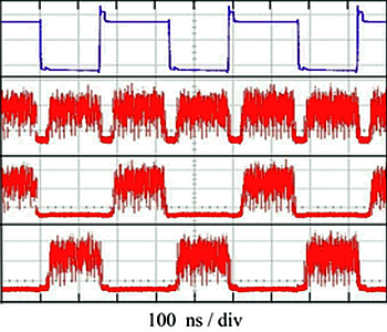
There are several attractive features of in-band optical labeling of high speed data packets. In this context in-band labeling describes the situation where the label is transmitted within the optical bandwidth of the data payload. The ability to route packets with imbedded labels in a single operation is attractive for keeping network complexity low. Imbedding the labels into the optical packet serves the purpose of reducing the bandwidth used for network signaling and eliminating the risk of label and data packet becoming de-correlated. In-band optical labeling in the schemes outlined here relies on modifying the spectrum of the optical data packet to accommodate the optical labels within the bandwidth otherwise occupied by the signal. As such, this kind of labeling is best suited for high-speed packet data where the perturbation of the optical signal spectrum caused by labeling will be small relative to the total extent of the signal spectrum. The minimum width of the labels (L1–L4 in Figure 1a) is limited by practical filtering schemes.
Figure 1. 
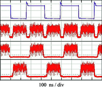
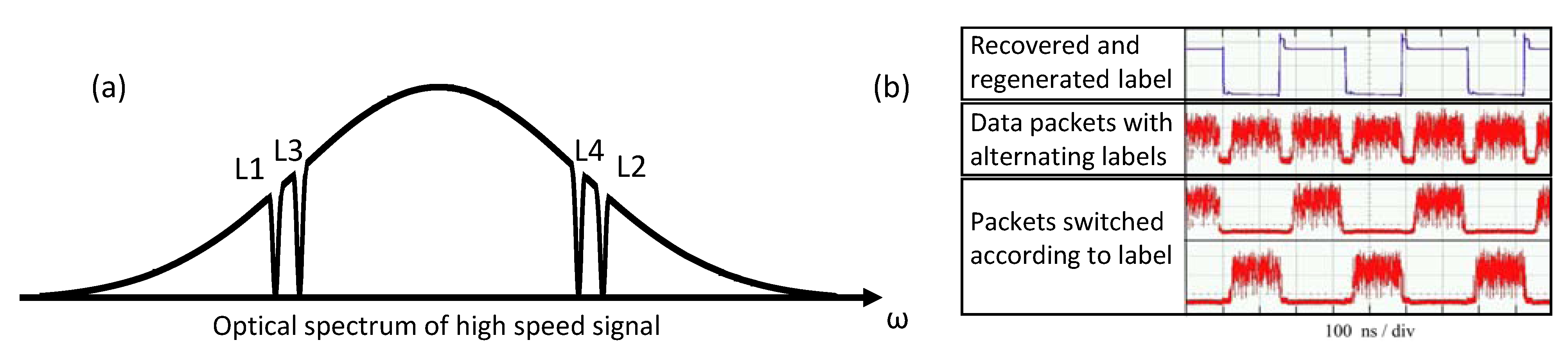
(a) Labeling of high speed data signals by spectral carving. L1–L4 indicate labeling positions where the presence or absence of power is interpreted as a digital label; (b) Results of labeling and switching 640 Gbit/s data packets.
Photonics 01 00083 g001
A simple scheme for in-band optical labeling is illustrated in Figure 1a. The labeling relies on frequency sub-bands inside the signal spectrum, where optical power can be suppressed to indicate a label “mark” or passed to indicate a “space”. In practice this is achieved by applying optical notch filters to shape the spectrum. As the labels encoded in this way rely on detecting small fractions of the actual signal spectrum, appropriate data scrambling is required to fulfill a mark-space ratio close to 50% in the data packet. This scheme has the clear advantage of keeping system complexity low since the labels are encoded by simple notch filtering and no extra signals are transmitted for labeling. In [3] it was verified that the scheme can be used to encode more than 60 logical labels while keeping the eye opening penalty less than 1 dB compared to the un-labeled data packet. The scheme has been shown in [4] to work for 640 Gbit/s data packets, where a single label was used to control a switch, separating labeled and unlabeled packets as shown in Figure 1b. As the scheme relies on detecting a fraction of the signal spectrum as a logical label, some regeneration of the amplitude of the detected label is required to extract a control signal suitable to drive an optical packet switch. This has been implemented using a simple electronic comparator circuit which regenerates the amplitude of the detected label and adds a fixed length to the label duration to ensure that stable and high-quality switching can be performed for every data bit in the packet. This fixed label padding is a few ns in this demonstration but can in principle be chosen freely according to the requirements of the label regenerator and switch. A packet guard interval of ~20 ns was used. In this demonstration the whole scheme could be implemented with a penalty of only 4 dB in receiver sensitivity of the labeled and switched data packet. Except for requiring slightly higher power into the receiver the signal could be detected with similar distribution in the performance of the 64 OTDM (optical TDM) channels compared with the un-labeled and un-switched signal.
It is expected that this labeling scheme could be particularly relevant in environments with high network complexity and relatively short transmission distances as is the case in e.g., data center networks.
A variation of the scheme mentioned above is demonstrated in [5] where narrow spectral bands in the broad data spectrum are allocated for transmission of optical labels. In this scheme optical labels are inserted into the assigned portions of the signal spectrum as low rate binary signals. Additionally, this scheme also allows for the insertion of a clock pilot signal which can be used for synchronizing the receiver to the incoming data packet relaxing the requirements for high-speed clock recovery circuits. High quality clock transmission does, however, require the optical spectrum of the data payload to be suppressed in the narrow spectral range where the clock is inserted. This scheme offers more freedom to adjust the duration and power of the optical labels. In this way the use of a regenerating circuit for the received labels can be avoided and the quality of the transmitted labels does not depend on scrambling of the data payload. This scheme does however require an optical transmitter for each optical label to be added. Consequently, complexity is moved from the receiver to the transmitter. One critical point in this labeling scheme is the relative stabilization of the filters used to extract the optical labels and the optical transmitters generating the labels. The wavelength stability of the label transmitters has to be carefully controlled.
This scheme has been demonstrated at 640 Gbit/s packet data rate with 50 km transmission to verify the performance of the transmitted pilot clock. Packet labeling and packet clock transmission was implemented in this demonstration. Only marginal phase noise was added by transmitting the clock as an in-band pilot clock increasing the total timing jitter (integrating the phase noise from 100 Hz to 10 MHz) from 80 fs to 90 fs. The quality of the transmitted labels allowed for switching the data packets with a penalty of ~1.5 dB in receiver sensitivity for achieving BER of 10−9, compared to the performance of unlabeled data packets.
Both packet labeling schemes mentioned above employ similar simple electronic circuits for detecting and processing the labels, imposing only a few ns of latency (<10 ns) when combined with the packet switching. Regarding dynamic allocation of labels to individual packets, both schemes require fast optical switching, similar to what is used for switching packets. This is used either to generate labels to be added to the signal in the case of the latter scheme or to switch the notch filters which the packet is subjected to in the case of the first scheme. In both cases the latency caused by label creation is expected to be even less than for label detection and processing.

2.2. Optical Labeling of TDM Data Channels

In very high speed TDM transmission it may be attractive to label the TDM channels in such a way that an optical receiver will be able to selectively receive only specific channels without having to have the capacity to receive the entire TDM data stream. In [
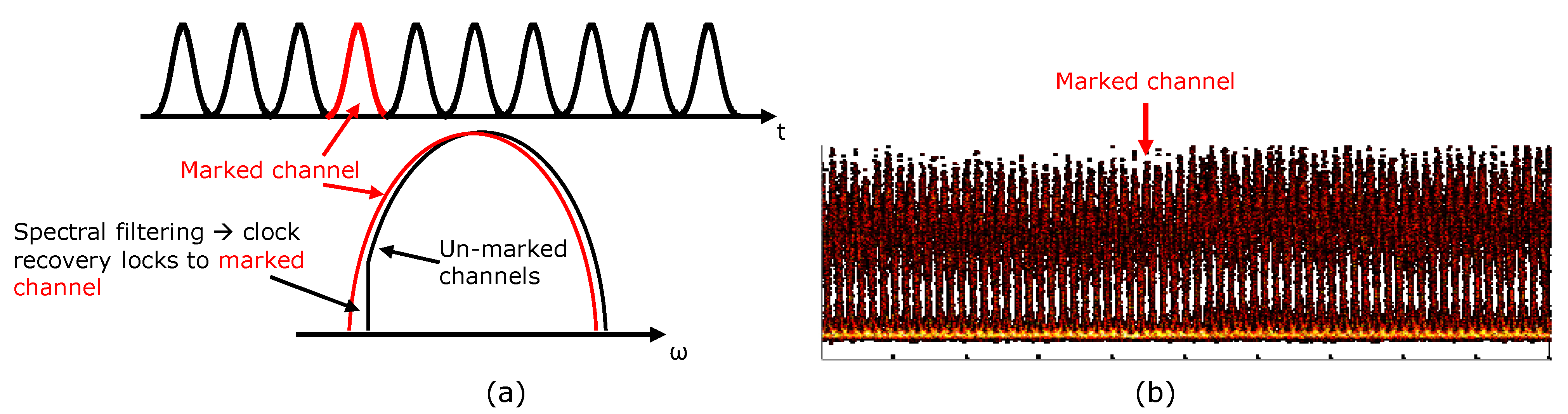
6] a scheme for labeling of a 650 Gbit/s OTDM data stream is proposed and demonstrated. In this scheme the optical spectrum of one of the OTDM tributary channels is slightly altered compared to the remaining channels, allowing a receiver to identify that channel and subsequently enumerate the remaining channels based on this reference channel. Also, detecting a single channel allows for a low rate (in this case 10 GHz) clock recovery circuit to be used to extract the base rate clock, which is required for extracting the tributary channels. This should be seen in contrast to the pre-scaled clock recovery discussed in Section 4. In this scheme no dedicated clock signal is transmitted alongside the data signal, eliminating the potential signal or clock degradation due to cross talk between several co-propagating signals. The clock signal, which is also used for channel identification, is extracted simply by tuning a band pass filter to one edge of the optical data spectrum as illustrated in Figure 2a.
Figure 2. (a) Principle of channel labeling by spectral shaping; (b) 650 Gbit/s data signal after 80 km transmission with marked channel indicated.
Photonics 01 00083 g002
The scheme is shown to work in an 80 km transmission demonstration of 650 Gbit/s data incorporating a fully polarization insensitive receiver. The transmitted 650 Gbit/s signal is shown in Figure 2b where the marked channel is also indicated. A slight penalty in receiver sensitivity of ~2 dB for achieving a BER of 10−9 is observed for the labeled channel compared to the remaining channels in back-to-back configuration. After 80 km transmission the labeled channel has similar performance to the remaining channels as Figure 2b would also indicate.
A main attraction of this labeling scheme is the low complexity of the setup in both generating and detecting the labels. Shaping the spectrum does alter the transmission properties of the channel slightly but it has been shown that this effect can be kept small while still achieving a detectable spectral change to the labeled channel.

2.3. Optical Switching of Data Packets

An attractive feature which is facilitated by the availability of optical packet labeling is optical packet switching. In optical packet switching data packets are switched and routed through a network without the need for o/e conversion of the entire data packet at every switching node. This is particularly attractive for high speed or very large data packets where detection and buffering requires significant resources. Significant benefit is expected if the data payload can be switched to the correct outlet port without requiring the switch to be able to process the full data payload. Optical packet switching has been realized in a number of different schemes. Two schemes will be briefly introduced in this section, having different properties and benefits.

2.4. Optical Packet Switching by Wavelength Conversion in a Si Waveguide

Optical packet switching can be combined with wavelength conversion in the scheme demonstrated in [
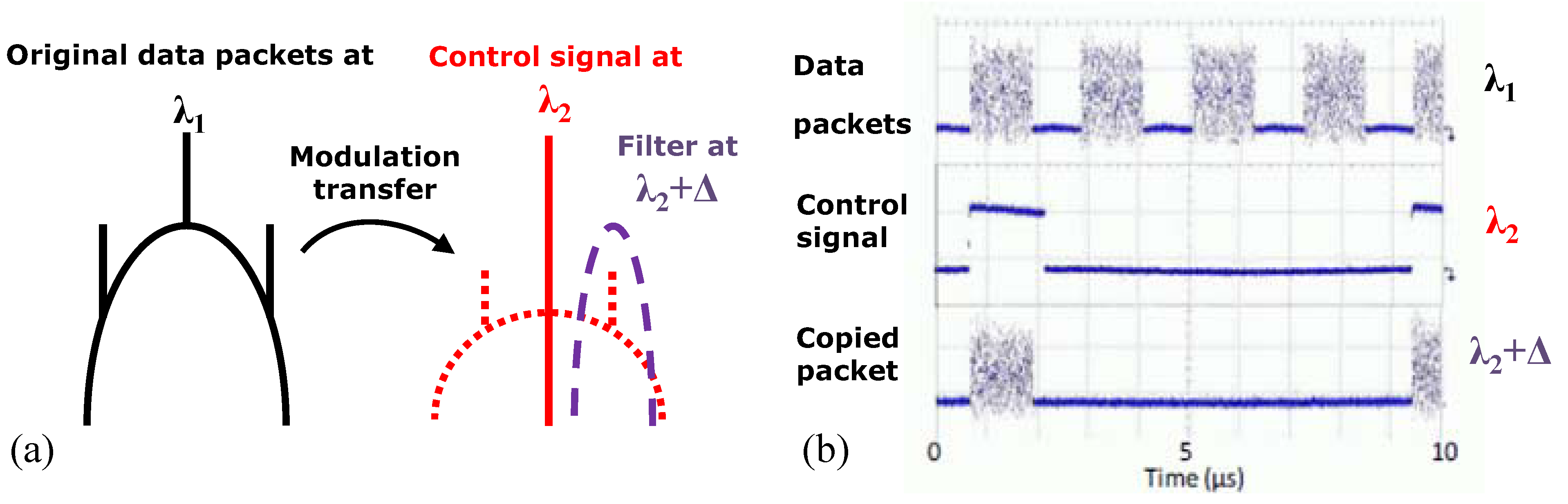
7]. In this scheme cross phase modulation (XPM) is used to transfer amplitude modulation between original data packets and a control signal. The presence of this control signal determines which data packets are switched to the wavelength of the control signal. It is important to note that the data packet is not erased at the original wavelength in this scheme. This adds a multicasting capability to the scheme, which may be desirable. Figure 3a shows the working principle of the packet switching by wavelength conversion. A control signal indicated at λ2 is selectively launched into a nonlinear device, in this case a silicon (Si) waveguide, to temporally overlap with the packet to be switched. The packet temporally aligned with the control signal is then wavelength converted by XPM and thus extracted from the original stream of packets as shown in Figure 3b. λ1 is the data packet stream before switching—acting as pump for the XPM. λ2 is the control signal used to select the packet to be switched—acting as probe for the XPM. λ2 + Δ is the filtered output copy of the selected data packet.
Figure 3. (a) Operating principle of packet switching by wavelength conversion and offset filtering; (b) Results of packet switching implementation in an 8 mm long Si nanowire.
Photonics 01 00083 g003
This scheme for optical packet switching has been shown to introduce ~2.5 dB of power penalty in the receiver sensitivity for a BER of 10−9 compared to the un-switched packets. The target wavelength of the switched packet can be chosen with some flexibility depending on the properties of the specific chosen nonlinear switching material.
Packet switching in this scheme is highly flexible. The nonlinear switching process is nearly instantaneous (based on Kerr nonlinearity) and the switching speed and the temporal resolution are limited only by the ability to generate appropriate optical control signals. One limitation of the packet switching scheme using wavelength conversion is the inability to remove the switched packet from the original packet flow. This prevents reusing time slots in the packet flow and may cause unnecessary traffic to be transmitted in parts of the network.

2.5. Optical Packet Switching in an Electro-Optic Switch

An alternate scheme for packet switching which has also been investigated and demonstrated, is switching of packets in an electro-optic switch [4]. In this scheme the packets remain at the same wavelength and switching is performed by transmitting or attenuating packets in the switch according to an applied electrical control signal. This scheme allows for reutilization of the cleared packet slots and is thus similar to packet routing based on o-e-o conversion. As electro-optic switches typically have limited modulation bandwidth, this scheme will require careful control of the guard interval between data packets and the electrical signal controlling the switch, as discussed below.
In [4], electro-optic packet switching is demonstrated in combination with the optical packet labeling scheme discussed in Section 2.1. The optical labels are detected for individual packets and used as control signal for the switch, which in this demonstration is a Lithium-Niobate (LN) Mach-Zehnder modulator (MZM) used as an on/off switch. The availability of high performance space switches would significantly improve the scaling potential of such optical switching schemes. Semiconductor-based circuits as e.g., [8] offer promising progress in this area in terms of switching speed and port count. In the current demonstration [4], scaling the scheme to a large number of outputs would incur a prohibitively large loss from splitting the signal to one switch for each output path. It is, however, clearly demonstrated that optical labels imbedded within data packets can be detected and used as control signals for an electro-optical switch achieving high-quality switching of the entire packet. This approach may offer attractive possibilities of combining control and transport layer infrastructure in optical networks.

3. Optical Synchronization of Data Packets

Optical synchronization of data packets to a master clock addresses a key limitation regarding global synchronization in complex optical networks. The key functionality of optical data synchronization is demonstrated in [9,10]. The scheme for optical data synchronization relies on carefully applying a timing-dependent phase modulation to the individual data bits and subsequently adjusting their relative timing using a dispersive element. Figure 4a illustrates the basic principle of the scheme.
Figure 4. (a) Illustration of the operating principle of optical data synchronization. Phase modulation (marked in blue) is applied to the data signal (marked in red) which is at a pulse rate slightly offset from the target clock frequency f. After propagation through a dispersive medium the data pulses acquire the pulse rate f (marked in black); (b) Result of multiplexing a synchronized data packet into a vacant time slot in a high speed data stream.
Photonics 01 00083 g004
This scheme has been demonstrated to work on data packets up to 12,144 bits for a frequency offset of 200 kHz. Data synchronization according to this scheme can correct the clock offset with such precision that the synchronized data can be TDM multiplexed into a data stream of pulses running at the reference frequency f, achieving a total aggregated pulse rate of 1.29 Tbit/s while still allowing for error free (BER < 10−9) detection of the synchronized data pulses. Figure 4b shows the multiplexing of the synchronized data packet into an empty time slot in a 1.29 Tbit/s OTDM signal. Precise synchronization and stable multiplexing is achieved.
It is important to notice that the data synchronization accomplished with this scheme is a localized phenomenon, meaning that the phase modulation transfers the frequency offset from the time domain to the frequency domain, allowing for synchronization to be achieved by adding a well-controlled amount of dispersion. Further dispersive propagation will cause the pulses to lose the synchronization to the clock f. In a larger optical network this synchronization scheme should ideally be combined with some means of canceling the spectral chirp caused by the phase modulation once synchronization is achieved. For amplitude modulated data this could e.g. be done by wavelength conversion by XPM as described in [11].

4. Ultra High Speed Clock Recovery

In network nodes where optical data aggregation and thus synchronization is not required a key functionality is the ability to recover a high fidelity clock, i.e., a clock signal with ultra-low phase noise, from a high speed data signal, which can be used in the optical TDM demultiplexing (equivalent to electrical de-serializing). In Section 2.2 a labeling scheme was discussed which circumvents this issue by embedding a label from which a clock signal can be directly extracted. However, for unlabeled data channels pre-scaled optical clock recovery is required in order to extract a sub-rate clock from a high speed data signal at bit rates beyond the bandwidth of electronic receivers. A few schemes have been demonstrated for clock recovery at bit rates as high as 640 Gbit/s. In [12] an injection locked loop containing a semiconductor optical amplifier (SOA) was demonstrated for 640 Gbit/s clock recovery. In [13] pre-scaled clock recovery is demonstrated for a data signal at 640 Gbit/s using nonlinear mixing in a periodically poled lithium niobate (PPLN) waveguide. An opto-electronic phase locked loop (PLL) is used to lock a local oscillator (LO) radio frequency (RF) clock source to a tributary channel in the high speed data signal. The optical mixing in the PPLN waveguide is used to achieve very high resolution phase comparison between pulses derived from the LO clock and pulses in the data signal. The mixing output is then detected and used for feedback control of the LO clock. The operating principle of the pre-scaled electro-optic PLL clock recovery is sketched in Figure 5.
Figure 5. Working principle of pre-scaled electro-optic clock recovery.
Photonics 01 00083 g005
This clock recovery scheme has been demonstrated in a transmission experiment in [14] to be able to recover a clock signal of sufficient high quality to enable detection of the transmitted 640 Gbit/s data signal with less than 1 dB penalty in receiver power to achieve a BER of 10−9. A recovered clock with timing jitter less than 100 fs could be derived from a transmitted 640 Gbit/s data signal using the clock recovery. This degree of synchronization is fully adequate even for bitrates as high as 640 Gbit/s.

5. Efficient Detection of Ultra-High-Speed Data Signals

A final functionality of vital importance to high speed optical networking is the ability to efficiently receive very high speed optical data signals. As mentioned earlier high speed data signals must be optically demultiplexed (or parallelized) before they can be handled by high speed electronic receivers. This optical demultiplexing of time interleaved signals has typically been addressed in the time domain by applying very short temporal gates which sample out single tributary channels at a significantly reduced rate. This approach has been demonstrated for pulse rates as high as 1.28 Tbaud using various optical switches like a nonlinear optical loop mirror (NOLM) [15]. An alternate scheme which has recently been investigated extensively relies on optical Fourier transformation (OFT) to convert the distinct data channels from the time domain into the frequency domain. This allows for conventional wavelength division multiplexing (WDM) receivers to be used for detection of high speed data signals. In the OFT scheme dispersion is used to broaden the short optical pulses and a following parabolic phase modulation compresses the spectrum of the individual short pulses at different central wavelengths determined by the temporal alignment between the pulse and the applied phase modulation. The concept of the OFT-based receiver is outlined in Figure 6.
Figure 6. Principle of optical Fourier transformation (OFT) for transferring short pulses in the time domain into separated spectra in the frequency domain.
Photonics 01 00083 g006
This scheme has been demonstrated mapping 10 Gbit/s tributary channels from a 640 Gbit/s data signal onto a 25 GHz WDM wavelength grid in [16]. A total of 40 channels could be converted simultaneously in a single OFT unit, however with significant performance penalty compared to conventional time gating of high speed signals. The OFT converted channels in this demonstration achieved a BER ~10−5. The main limitation in converting such a large number of channels from a high speed data signal is the requirements to the optical mixing platform which performs the phase modulation (PM) shown in Figure 6. In this demonstration phase modulation was achieved by four wave mixing (FWM) of the data signal with a chirped pump signal. In this way phase modulation with large modulation index can be achieved, however efficient FWM over a large wavelength range is required. To achieve the large FWM bandwidth a dispersion-engineered Si waveguide was used in this demonstration. These devices can achieve very large FWM bandwidth but suffer from low FWM efficiency. This is the main cause for the severe signal degradation observed in the serial-to-parallel conversion. The OFT-based scheme for serial-to-parallel conversion holds great potential compared to the time-domain gating approach since a large number of channels can be processed simultaneously by the use of a single optical control pulse and subsequently demultiplexed using WDM de-multiplexers. It has been shown numerically in [17] that there is not an inherent performance penalty associated with the OFT scheme compared to the time gating, whereas the total power spent on switching the cannels is significantly lower when using serial-to-parallel conversion. The implementation penalty associated with the use of OFT for serial-to-parallel conversion is continuously being improved and recently error free signal detection was achieved for converting 10 Gbit/s tributary channels from a 1.28 Tbit/s serial data signal into WDM channels [18]. This was achieved in highly nonlinear fiber by reducing the number of converted channels. In [19] extension of the OFT scheme to convert all channels in a data stream simultaneously has been investigated. It is shown that this is possible at 160 Gbit/s at the expense of additional performance penalties on certain tributary channels.

6. Discussion and Conclusions

In the previous sections some key functionalities and demonstrations relevant for achieving ultra-high-speed optical networking have been described and discussed. Significant advances have been made in this field and many key system elements are already demonstrated. At the pulse repetition rates addressed here, literally hundreds of GHz, many system functionalities rely strongly on nonlinear optical signals processing. This is enabled by the availability of very high quality platforms for optical signal processing including nonlinear waveguides and nonlinear optical fiber. Nonlinear optical signal processing has yet to experience any substantial market penetration but a number of schemes for high speed signal processing are available and are continuously being improved and expanded.
The schemes and functionalities outlined in this paper already enable fairly sophisticated high speed optical networking. In a packet based network packet labeling, packet synchronization and packet switching have been demonstrated. In a TDM based transmission system channel identification and clock recovery have been demonstrated. Relevant for both cases is the demonstrated ability to perform highly efficient detection of these very high data rates by serial-to-parallel conversion.

Acknowledgments

OFS Denmark is acknowledged for providing the optical fiber used in the demonstrations discussed in this paper. This work was supported by the European Research Council (ERC) Starter Grant project SOCRATES (ref. no. 240467). This work was supported by the Danish Research Council grant for Terabit Ethernet on Silicon Photonic Chips.

Author Contributions

Writing of paper: Michael Galili. Comments and feedback: Anders Clausen. Experimental investigations: Michael Galili, Hao Hu, Hans Christian Hansen Mulvad, Ashenafi Kiros Medhin. Schemes and design of investigations: Michael Galili, Hao Hu, Hans Christian Hansen Mulvad, Ashenafi Kiros Medhin, Leif Katsuo Oxenløwe.

Conflicts of Interest

The authors declare no conflict of interest.

References

  1. Namiki, S.; Hasama, T.; Ishikawa, H. Optical signal processing for energy-efficient dynamic optical path networks. In Proceedings of the 36th European Conference and Exhibition on Optical Communication (ECOC), Torino, Italy, 19–23 September 2010; pp. 1–6.
  2. Tucker, R.S. Optical packet-switched wdm networks—A cost and energy perspective. In Proceedings of the Optical Fiber Communication Conference (OFC), San Diego, CA, USA, 24–28 February 2008. paper OMG1.
  3. Mehdin, A.K.; Galili, M.; Oxenløwe, L.K. Novel Optical Labeling Scheme for Ultra-High Bit Rate Data Packets. In Proceedings of the OptoElectronics and Communications Conference (OECC), Kyoto, Japan, 30 June 2013–4 July 2013; pp. 1–2.
  4. Medhin, A.K.; Galili, M.; Oxenløwe, L.K. 640 Gbit/s optical packet switching using a novel in-band optical notch-filter labeling scheme. In Proceedings of the Optical Fiber Communication Conference (OFC), San Francisco, CA, USA, 9–13 March 2014.
  5. Gomez-Agis, F.; Hu, H.; Luo, J.; Hansen Mulvad, H.C.; Galili, M.; Calabretta, N.; Oxenløwe, L.K.; Dorren, H.; Jeppesen, P. Optical switching and detection of 640 Gbits/s optical time-division multiplexed data packets transmitted over 50 km of fiber. Opt. Lett. 2011, 36, 3473–3475. [Google Scholar] [CrossRef]
  6. Galili, M.; Hansen Mulvad, H.C.; Hu, H.; Oxenløwe, L.K.; Gomez-Agis, F.; Ware, C.; Erasme, D.; Clausen, A.; Jeppesen, P. 650 Gbit/s OTDM Transmission over 80 km SSMF Incorporating Clock Recovery, Channel Identification and Demultiplexing in a Polarisation Insensitive Receiver. In Proceedings of the Optical Fiber Communication Conference (OFC), San Diego, CA, USA, 21–25 March 2010; pp. 1–3.
  7. Hu, H.; Galili, M.; Pu, M.; Yvind, K.; Jeppesen, P.; Oxenløwe, L.K. 160 Gbit/s optical packet switching using a silicon chip. In Proceedings of the IEEE Photonics Conference, Burlingame, CA, USA, 23–27 September 2012; pp. 915–916.
  8. Varrazza, R.; Djordjevic, I.B.; Yu, S. Active Vertical-Coupler-Based Optical Crosspoint Switch Matrix for Optical Packet-Switching Applications. J. Lightw. Technol. 2004, 22, 2034–2042. [Google Scholar] [CrossRef]
  9. Hu, H.; Areal, J.L.; Hansen Mulvad, H.C.; Galili, M.; Dalgaard, K.; Palushani, E.; Clausen, A.; Berger, M.S.; Jeppesen, P.; Oxenløwe, L.K. Synchronization, retiming and time-division multiplexing of an asynchronous 10 Gigabit NRZ Ethernet packet to terabit Ethernet. Opt. Express 2011, 19, B931–B937. [Google Scholar] [CrossRef]
  10. Hu, H.; Areal, J.L.; Palushani, E.; Oxenløwe, L.K.; Clausen, A.; Berger, M.S.; Jeppesen, P. Optical Synchronization of a 10-G Ethernet Packet and Time-Division Multiplexing to a 50-Gb/s Signal Using an Optical Time Lens. IEEE Photonics Technol. Lett. 2010, 22, 1583–1585. [Google Scholar] [CrossRef]
  11. Galili, M.; Oxenløwe, L.K.; Hansen Mulvad, H.C.; Clausen, A.T.; Jeppesen, P. Optical wavelength conversion by cross-phase modulation of data signals up to 640 Gb/s. J. Sel. Top. Quantum Electron. 2008, 14, 573–578. [Google Scholar] [CrossRef]
  12. Hansen Mulvad, H.C.; Tangdiongga, E.; Waardt, H.d.; Dorren, H. 40 GHz clock recovery from 640 Gbit/s OTDM signal using SOA-based phase comparator. Electron. Lett. 2008, 44, 146–148. [Google Scholar] [CrossRef]
  13. Oxenløwe, L.K.; Gomez Agis, F.; Ware, C.; Kurimura, S.; Hansen Mulvad, H.C.; Galili, M.; Kitamura, K.; Nakajima, H.; Ichikawa, J.; Erasme, D.; et al. 640 Gbit/s clock recovery using periodically poled lithium niobate. Electron. Lett. 2008, 44, 370–372. [Google Scholar] [CrossRef]
  14. Oxenløwe, L.K.; Gómez-Agis, F.; Ware, C.; Kurimura, S.; Hansen Mulvad, H.C.; Galili, M.; Nakajima, H.; Ichikawa, J.; Erasme, D.; Clausen, A.T.; et al. 640-Gbit/s Data Transmission and Clock Recovery Using an Ultrafast Periodically Poled Lithium Niobate Device. J. Lightw. Technol. 2009, 27, 205–213. [Google Scholar] [CrossRef]
  15. Hansen Mulvad, H.C.; Oxenløwe, L.K.; Galili, M.; Grüner-Nielsen, L.; Jeppesen, P. 1.28 Tbit/s single-polarisation serial OOK optical data generation and demultiplexing. Electron. Lett. 2009, 45, 280–281. [Google Scholar] [CrossRef]
  16. Hansen Mulvad, H.C.; Palushani, E.; Hu, H.; Ji, H.; Lillieholm, M.; Galili, M.; Clausen, A.T.; Pu, M.; Yvind, K.; Hvam, J.M.; et al. Ultra-high-speed optical serial-to-parallel data conversion by time-domain optical Fourier transformation in a silicon nanowire. Opt. Express 2011, 19, B825–B835. [Google Scholar] [CrossRef]
  17. Lillieholm, M.; Hansen Mulvad, H.C.; Palushani, E.; Peucheret, C.; Jeppesen, P.; Oxenløwe, L.K. Numerical investigation of power requirements for ultra-high-speed serial-to-parallel conversion. In Proceedings of the IEEE Photonics Conference (IPC), Burlingame, CA, USA, 23–27 September 2012; pp. 110–111.
  18. Hu, H.; Kong, D.; Palushani, E.; Andersen, J.D.; Rasmussen, A.; Sørensen, B.M.; Galili, M.; Hansen Mulvad, H.C.; Larsen, K.J.; Forchhammer, S.; et al. 1.28 Tbaud Nyquist Signal Transmission using Time-Domain Optical Fourier Transformation based Receiver. In Proceedings of the Conference on Lasers and Electro-Optics (CLEO), San Jose, CA, USA, 9–14 June 2013.
  19. Petrillo, K.G.; Foster, M.A. Full 160-Gb/s OTDM to 16x10-Gb/s WDM conversion with a single nonlinear interaction. Opt. Express 2013, 21, 508–518. [Google Scholar] [CrossRef]

