Article

Tailoring Upconversion and Morphology of Yb/Eu Doped Y2O3 Nanostructures by Acid Composition Mediation

1
i3N/CENIMAT, Department of Materials Science, Faculty of Sciences and Technology, Universidade NOVA de Lisboa and CEMOP/UNINOVA, Campus de Caparica, 2829-516 Caparica, Portugal
2
INCM, Imprensa Nacional-Casa da Moeda, Av. António José de Almeida, 1000-042 Lisboa, Portugal
3
SINTEF Materials Physics, Forskningvein 1, 0373 Oslo, Norway
*
Authors to whom correspondence should be addressed.
Nanomaterials 2019, 9(2), 234; https://doi.org/10.3390/nano9020234
Submission received: 29 December 2018 / Revised: 23 January 2019 / Accepted: 4 February 2019 / Published: 9 February 2019

Abstract

:
The present study reports the production of upconverter nanostructures composed by a yttrium oxide host matrix co-doped with ytterbium and europium, i.e., Y2O3:Yb3+/Eu3+. These nanostructures were formed through the dissociation of yttrium, ytterbium and europium oxides using acetic, hydrochloric and nitric acids, followed by a fast hydrothermal method assisted by microwave irradiation and subsequent calcination process. Structural characterization has been carried out by X-ray diffraction (XRD), scanning transmission electron microscopy (STEM) and scanning electron microscopy (SEM) both coupled with energy dispersive X-ray spectroscopy (EDS). The acid used for dissociation of the primary oxides played a crucial role on the morphology of the nanostructures. The acetic-based nanostructures resulted in nanosheets in the micrometer range, with thickness of around 50 nm, while hydrochloric and nitric resulted in sphere-shaped nanostructures. The produced nanostructures revealed a homogeneous distribution of the doping elements. The thermal behaviour of the materials has been investigated with in situ X-Ray diffraction and differential scanning calorimetry (DSC) experiments. Moreover, the optical band gaps of all materials were determined from diffuse reflectance spectroscopy, and their photoluminescence behaviour has been accessed showing significant differences depending on the acid used, which can directly influence their upconversion performance.

Graphical Abstract

1. Introduction

Upconverter materials are characterized by having the ability to emit photons with higher energy than the photons that were absorbed [1]. The most studied upconverters use rare earth doped luminescent materials. Rare earth elements belong to the lanthanides group in the periodic table and typically are trivalent ions (Ln3+) in which the 4f inner shell is filled up to 14 electrons, presenting a 4fn5s25p6 electron configuration (with n = 0–14) [1]. The partial filled 4f shell is the responsible for the optical and magnetic properties presented by this type of materials, and for the generation of radiation of different wavelengths, depending on the dopants used [2]. The most common used lanthanides elements are: Eu2+ and Ce3+ (broad band emitting due to the 5d → 4f transition) and Eu3+, Tb3+, Gd3+, Yb3+, Dy3+, Sm3+, Tm3+, Er3+, and Nd3+ (narrow band emitting due to transitions between 4f levels) [3]. Most of them present visible emissions, and some are described in Table 1 [4,5,6].
In the past few years, these rare earth oxides have attracted an increasing attention due to their possible use in several applications such as luminescence devices [7,8], color displays [9,10], optical detectors [11,12], telecommunications [5], upconverter lasers and photonics [13,14,15], catalysis [16], biomedicine [17,18] and solar cells [1,19,20], mainly due to their chemical, electronic, and optical properties resulting from the 4f electronic shells [21]. These properties are greatly dependent on the crystal structure, morphology and also on the chemical composition (type of dopants used), which are very sensitive to the bonding states of rare earth ions [21].
Yttrium oxide, Y2O3, is a rare earth oxide with a relatively high band gap value, around 5.8 eV [22], low phonon frequency and ionic radii [2]. Y2O3 is considered to be one of the greatest luminescent oxide phosphor materials available, mainly due to its high luminescence efficiency, chemical, thermal and photochemical stabilities but also due to its high color purity [23,24,25], presenting a large dielectric constant and good infrared transmission [22].
Y2O3 is a host material (matrix) and its wide band gap makes it attractive for several optical applications in the visible and UV ranges. Doping Y2O3 with other rare earth elements can bring some advantages, since they can emit within its optical window and not suffer quenching effects [26].
Ytterbium, Yb3+ is often used as a sensitizer due to its higher absorption cross-section that corresponds to 980 nm excitation, which will excite other elements like europium, Eu3+ [2]. Europium, on the other hand, is a trivalent material that contains ions from the rare earth and from the transition-metal series [27]. Doping Y2O3 with Eu3+ is considered to be one of the best red oxide phosphors due to their chemical stabilities and luminescence efficiencies [21,23]. The visible emission spectrum of Eu3+ is composed by 5D07F2, 5D07F1 and 5D07F0 [4]. The ratio between transitions 5D07F2 and 5D07F1 intensities, is an indicative of the resulting emission color. The higher the ratio, the more intense into the orange color will be the luminescence [4].
Y2O3 nanoparticles doped with Yb3+ and Eu3+ ions are expected to possess the ability to absorb near-infrared radiations (NIR) and upconvert it into visible radiation [28]. Yb3+ will work as a sensitizer (possessing one energy level around 980 nm, with a lifetime of ~2 ms, ideal for infrared to visible upconvertion), that will transfer the NIR energy to the activator Eu3+, with an emission wavelength shorter than the NIR excitation [1,28].
In terms of nanostructure shape, the synthesis of nanosized spherical phosphors particles brings the advantage of enhanced brightness and high resolution in upconversion applications [29], but also high packing densities and low light scattering. Therefore, it is suggested that the ideal morphology for a phosphor nanoparticle is a perfect spherical shape, with a narrow size distribution [29]. Several methods have already been reported for the synthesis of phosphors Y2O3 nanostructures aiming to obtain spherical shaped particles with homogeneous sizes and distributions, such as spray pyrolysis [23], sol-gel [30,31], hydrothermal/solvothermal methods [29], solution combustion [32,33], precipitation [34,35,36] and template method. Microwave assisted synthesis has also been reported for the production of Y2O3 materials [24,37,38], having numerous advantages, such as its celerity, reproducibility and cost-efficiency, in such a way that in the last few years it has been widely used on the synthesis of this oxide and several other types of oxides [39,40,41].
The present work focuses on the dissociation of primary oxides using different acids and further microwave synthesis of nanostructures based on Y2O3 doped with Yb and Eu. This synthesis route required minimal time to effectively dope the nanostructured matrix (15 min), which makes this a fast approach to produce such materials. The obtained nanostructures were fully characterized by X-ray diffraction (XRD), scanning transmission electron microscopy (STEM) and scanning electron microscopy (SEM), differential scanning calorimetry (DSC), Ultra Violet- Visible – Near Infrared (UV-VIS-NIR) spectroscopy, and photoluminescence.

2. Synthesis and Characterization of Yb/Eu Doped Y2O3 Nanostructures

2.1. Materials

The influence of different acids on the production of upconverter nanostructures under microwave irradiation was studied. For all the materials produced, the microwave synthesis was repeated at least 3 times for each set of samples produced, showing that this technique is highly reproducible, and presenting, within each set, the same type of structure, morphology and composition.
Regardless of the chosen acid, the basis of this synthesis is composed by a host matrix of yttrium oxide (Y2O3, CAS: 1314-36-9, purity 99.99%, with a particle size < 50 nm, from Sigma Aldrich, (Sigma-Aldrich Chemie Gmbh, Munich, Germany), and the dopants coming from the ytterbium oxide (Yb2O3, CAS: 1314-37-0, purity 99.7%, with a particle size < 100 nm, from Sigma Aldrich) and europium oxide (Eu2O3, CAS: 1308-96-9, purity 99.5%, with a particle size < 150 nm, from Sigma Aldrich), here named as the primary oxides. Several different acids have been used to dissolve the primary oxides and convert them to the form of nitrates: acetic acid (CH3COOH, CAS: 64-19-7, from Fisher Chemical (Fisher Scientific GmbH, Schwerte, Germany), hydrochloric acid (HCl, CAS: 7647-01-0, 37%, from Fisher Chemical) and nitric acid (HNO3 CAS: 7697-37-2, 69%, from Labkem(Blanc-Labo SA, Lonay, Switzerland). All the initial chemicals were used without further purification.

2.2. Yb/Eu Doped Y2O3 Synthesis

Three solutions were prepared, each of them with a different acid, i.e., acetic, hydrochloric and nitric acids. In this way, it became possible to study the influence of different acids compositions in the final materials’ outcomes, resorting to a hydrothermal synthesis assisted by microwave irradiation.
In a typical synthesis, 0.05 M of Y2O3, 0.01 M of YbO3 and 0.0075 M of Eu2O3 were diluted in 5 mL of acid (CH3COOH, HCl or HNO3), resulting in the formation of a colorless solution. The solution was kept under stirring on a hot plate at 70 °C in ambient atmosphere, until complete evaporation. A white powder was then obtained.
Afterwards, 40 mL of H2O and a most common used catalyst [2,42,43,44,45] was added to this powder and left stir for 10 minutes until complete dissociation. The solution was then placed in a Pyrex vessel and placed into a microwave heating system, Discover SP, from CEM (CEM Corporation, Matthews, NC, USA), fixing the maximum power up to 100 W with a temperature of 130 °C and 15 min synthesis time.
The obtained powders were then washed with deionized water and isopropyl alcohol. Between each washing process, the powder was centrifuged at 3000 rpm for 3 min. The annealing of the obtained nanostructures was carried out in a Nabertherm furnace (Nabertherm GmbH, Lilienthal, Germany), at a temperature of 700 °C for 6 h, under atmospheric conditions, with a heating ramp of 1 h. Figure 1 shows a schematic of Yb/Eu doped Y2O3 nanostructures production steps.

2.3. Yb/Eu Doped Y2O3 Characterization

All the characterization measurements were carried out in the powder form. The crystallinity and phase purity of as-synthesized and annealed materials were characterized by X-ray diffraction, using a PANalytical’s X’Pert PRO MRD X-ray diffractometer (PANalytical B.V., Almero, The Netherlands), with a monochromatic CuKα, λ = 1.540598 Å, radiation source. The XRD measurements were carried out from 25° to 60°, with a scanning step size of 0.016°. The in situ diffractograms were collected in the same 2θ range and at temperatures in steps of 100 °C, from 300 °C to 1000 °C. The material was kept at each temperature step for at least half an hour to allow the stabilization and 5 consecutive scans were collected for inspection of structural modifications during this time. The temperature was increased with a rate of ~1.7 °C min−1.
Differential Scanning Calorimetry measurements were carried out to the obtained powder, before annealing. It was used a simultaneous thermogravimetric analyzer, TGA-DSC-STA 449 F3 Jupiter, from Netzsch (Netzsch-Geratebau GmnH, Selb, Germany). Approximately 5 mg of powder was loaded into an open PtRh crucible and heated from room temperature to 1100 °C, with a heating rate of 10 °C min−1 under atmospheric conditions.
The morphology of all materials was analyzed by using a Scanning Electron Microscope (SEM) Carl Zeiss AURIGA CrossBeam Workstation instrument (Carl Zeiss Microscopy GmbH, Oberkochen, Germany), equipped with an Oxford energy dispersive X-ray spectrometer (EDS, Oxford Instruments Nanoanalysis, High Wycombe, UK).
Scanning Transmission Electron Microscopy (STEM) analyses of the nanostructures were carried out at 300 kV with a FEI Titan G2 60-300 instrument (Thermo Fisher Scientific, Hillsboro, OR, USA) equipped with a DCOR probe Cs-aberration corrector and a Super-X Bruker energy dispersive spectrometer with 4 silicon drift detectors. The size of 40 individual nanocrystals was determined through STEM images using ImageJ software (version 1.52k) [46].
For band gap determination, diffuse reflectance measurements were carried out at room temperature, using a Perkin Elmer lambda 950 UV/VIS/NIR spectrophotometer (Perkin Elmer, Inc., Waltham, MA, USA), with a diffuse light detection module (150 mm diameter integrating sphere, internally coated with Spectralon). The calibration of the system was performed by using a standard reflector sample (reflectance, R, of 1.00 from Spectralon disk). The reflectance (R) spectra was acquired in the range between 175 and 1200 nm.
Photoluminescence were also examined with a 976 nm laser (Avantes NIR light, Iso-Tech power source 1 W, 5 nm resolution) between 500 and 750 nm. All measurements were carried out under identical excitation/detection conditions, and for properly comparison of the PL intensities, the powder was weighted and pressed under the same pressure to obtain the same powder density.

3. Results and Discussion

The reactions between the different acids and the host matrix oxide (Y2O3) can be described by the following Equations (from 1 to 3) [47,48]:
Acetic   acid : Y 2 O 3 + 2 C H 3 C O O H + H 2 O ( Y ( C H 3 C O O ) ( O H ) 2 ) 2
Hydrochloric   acid : Y 2 O 3 + 3 H C l Y C l 3 + Y ( O H ) 3
Nitric   acid : Y 2 O 3 + 6 H N O 3 2 Y ( N O 3 ) 3 + 3 H 2 O
By mixing the catalyst to the yttrium ions obtained from the previous reactions, yttrium hydroxycarbonate is formed (Equation (4)). After microwave irradiation, it is observed the formation of yttrium oxycarbonate (Equation (5)). The powder formed is thus subjected to the final calcination step, in which the yttrium oxide nanostructures are obtained (Equation (6)) [43,45]:
2 Y 3 + + 7 H 2 O + 3 C H 4 N 2 O 2 Y O H C O 3 + 4 N H 4 + + C O 2
2 Y O H C O 3 S y n t h e s i s Y 2 O 2 C O 3 + H 2 O + C O 2
Y 2 O 2 C O 3 a n n e a l i n g Y 2 O 3 + C O 2

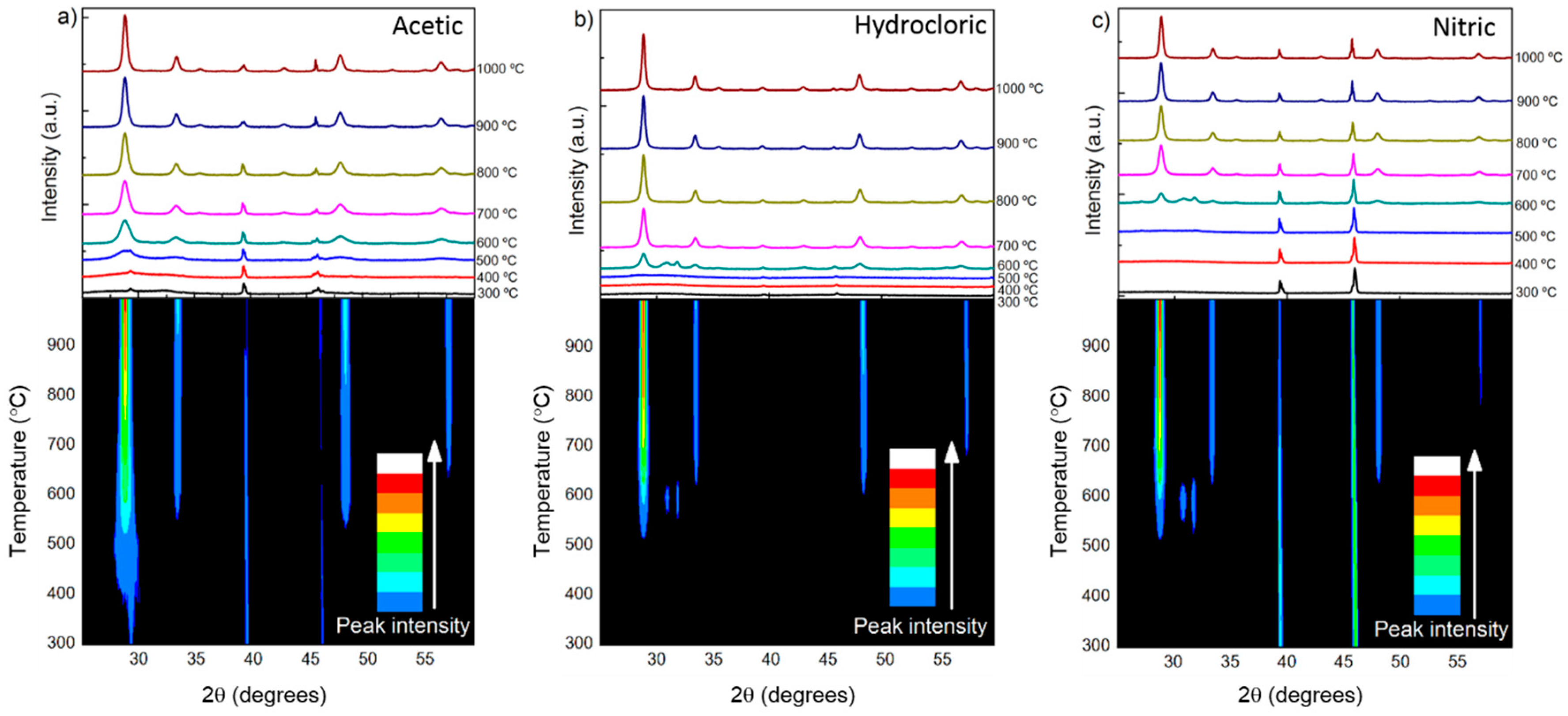
3.1. Structural Characterization of Yb/Eu Doped Y2O3 Nanostructures

Figure 2 shows the XRD diffractograms of the nanostructures obtained by microwave synthesis, when using different acids for the dissociations of the primary oxides, and before any heat treatment. It is possible to observe that the as-synthesized nanostructures are amorphous when using hydrochloric and nitric acid. Regarding the use of acetic acid, the synthesized nanostructures present some degree of crystallinity.
To find out the temperature at which there was an amorphous to crystalline phase transformation, in situ XRD analyses were carried out in the temperature range from 300 °C to 1000 °C. From the annealing process, in 100 °C steps, it is expected to complete the formation of crystalline Yb/Eu doped Y2O3 nanostructures from the intermediate products and sesquioxide phases of Y2−xO3−x [23], as the temperature is raised. On Figure 3, it is possible to observe the XRD diffractograms evolution with the increase of temperature and the respective contour plot, for the Yb/Eu doped Y2O3 nanostructures produced using all three acids. It can be observed that for all materials, the complete phase shift to crystalline Y2O3 occurs at 700 °C, without expressive changes up to 1000 °C.
Figure 4 shows the XRD diffractograms of Yb/Eu doped Y2O3 nanostructures, prepared with different types of acids, and annealed at 700 °C, for 6 h. For comparison, the XRD simulated Y2O3 powder pattern is also shown. It is possible to observe that regardless the used acid, after calcination, it was obtained crystalline Y2O3 nanostructures, having a cubic type structure, with the main reflections being (222), (400), (440) and (622), which is in accordance to the literature [23,42]. No peaks shift, or other impurity phases were detected, indicating that a high purity Yb/Eu doped Y2O3 nanostructures were obtained by annealing at 700 °C for 6 h.
The crystallite size, D, was estimated using the Scherrer’s equation and the most intense peak, corresponding to (222) plane [37]:
D = 0.9   λ B c o s θ
where λ is the X-ray wavelength (corresponding to Cu Kα radiation—1.540598 Å), B is the full width at half-maximum (FWHM) in radian and θ is the Bragg diffraction angle degrees. It was obtained a crystallite size of 16.12 nm, 21.88 and 19.86 nm for synthesis with acetic, hydrochloric and nitric acids, respectively.
In order to understand the different transformations that occur during Yb/Eu doped Y2O3 calcination, differential scanning calorimetric measurements were carried out for all materials. The results are shown in Figure 5. The microwave synthesized materials, which consist in yttrium oxycarbonates were analyzed and it is possible to observe a small mass loss before 110–200 °C, that corresponds to a possible vaporization of the sorbet water. The second weight loss step, below 400–510 °C can be attributed to a dehydration of the yttrium oxycarbotates. The complete conversion into Y2O3 occurs at temperatures between 400 and 800 °C corresponding to a mass loss step of 20% for hydrochloric and nitric acid and only 12% for acetic acid. This mass loss is accompanied by an endothermic peak centered at 611–650 °C. Above this temperature, no other weight loss steps or peaks are observed, indicating that the complete conversion of the yttrium oxycarbonate into Y2O3 has occurred. These results are in agreement to what is described in literature [45,48] and to what was observed on in situ XRD results (Figure 3). These results justify the selected calcination temperature used in the present study, since above 700 °C, no other phase transformation could be detected.
SEM and STEM analyses were carried out for all the materials produced. Figure 6 shows SEM images of the materials after microwave synthesis and before and after calcination. As can be seen, the shape of the nanostructures is maintained after calcination. Nevertheless, after heat exposure, the shape of such structures is better defined, especially for the nitric-based structures. When comparing the three acids used, it is evident that the acetic acid resulted in thin nanosheets, while both hydrochloric and nitric resulted in perfect sphere-like structures (Figure 6 and Figure 7). It is also clear that after calcination, it is observed a reduced diameter that can be explained by sintering, where small primary single crystals diffuse across the boundaries and coalescence to form a larger one. The total volume decreased because a densely packed with the elimination of pores was formed.
The nanosheets had an average size of ~2.5 μm and thickness of ~50 nm, while the size of the spheres varied with the acid used. For the hydrochloric acid, the structures had 192 ± 25 nm, and for the nitric, it has been measured an average size of 216 ± 37 nm. Nevertheless, both hydrochloric and nitric-based materials revealed heterogeneities in sphere sizes (this can be observed by the presence of smaller spheres). From Figure 7e,f, it can be observed that the spheres are composed by smaller primary grains, joined to form a compact/granular spherical structure [49]. These smaller grains may justify the crystallite sizes measured by XRD.
EDS measurements were also carried out on both nanostructures formed (see Figure 8). Both nanosheets and spheres showed the presence of Y, Yb, Eu, and O well distributed along the structures. This indicates that the doped Yb3+ and Eu3+ were successfully incorporated into the Y2O3 host matrix. Moreover, these results are in agreement to XRD, where no second phases were detected.
The possible reasons for these morphological differences in the nanostructures studied are expected to be due to a group of distinct factors. Indeed, the shape of Y2O3 nanostructures can be greatly influenced by factors such as intrinsic crystal/cluster structure configuration, precursors, catalysts, surfactants and also by synthesis temperature and time [50]. However, it is believed that the catalyst is responsible for the final nanostructures’ morphology. The decomposition of the catalyst into ammonia and carbonates ions (OH and CO32− ions) originates a homogeneous nucleation of Y2O3 nanostructures occurring a spontaneous aggregation process in order to minimize the surface energy, forming sphere-shaped nanostructures [50,51]. These spherical nanostructures are an intermediate step in the morphological evolution into nanosheets structures. By increasing the amount of catalyst or by increasing the synthesis time, the dissolution–recrystallization equilibrium will cause the dissolution of smaller particles and the anisotropically grow of larger particles (into sheets) during the Ostwald ripening period [50]. Liu et al. [52] synthesized Y2O3:Eu3+ nanospheres and by increasing synthesis time while keeping constant the catalyst concentration, they obtained nanoparticles with irregular shape. Khachatourian et al. [51] also studied the effect of catalyst on the morphology of Y2O3 nanoparticles. They observed that by increasing the catalyst into a critical point, the diameter nanosphere would decrease (a higher degree of supersaturation would lead into a burst formation of nuclei due to the presence of a higher quantity of OH and CO32− ions, originating a decrease on particle size). Above that point it would result in larger particles [51]. A higher concentration of catalyst will act both as hydrogen-bond donors and acceptors (through C=O groups), resulting in self-association into two-dimensional layered frameworks (sheets nanostructures) [50,53].
By using carboxylic acid (such as acetic acid), it is possible to synthesize a series of nanocrystals connected orthogonally by hydrogen-bonded NH chains and carboxylic acid dimers, and by this way design two-dimensional layered networks [53]. In the case of the other acids tested, hydrochloric and nitric acids resulted in sphere-like structures—but with differences in size—which can be expected since the dissociation reaction of primary oxides should be different regarding the acid used.

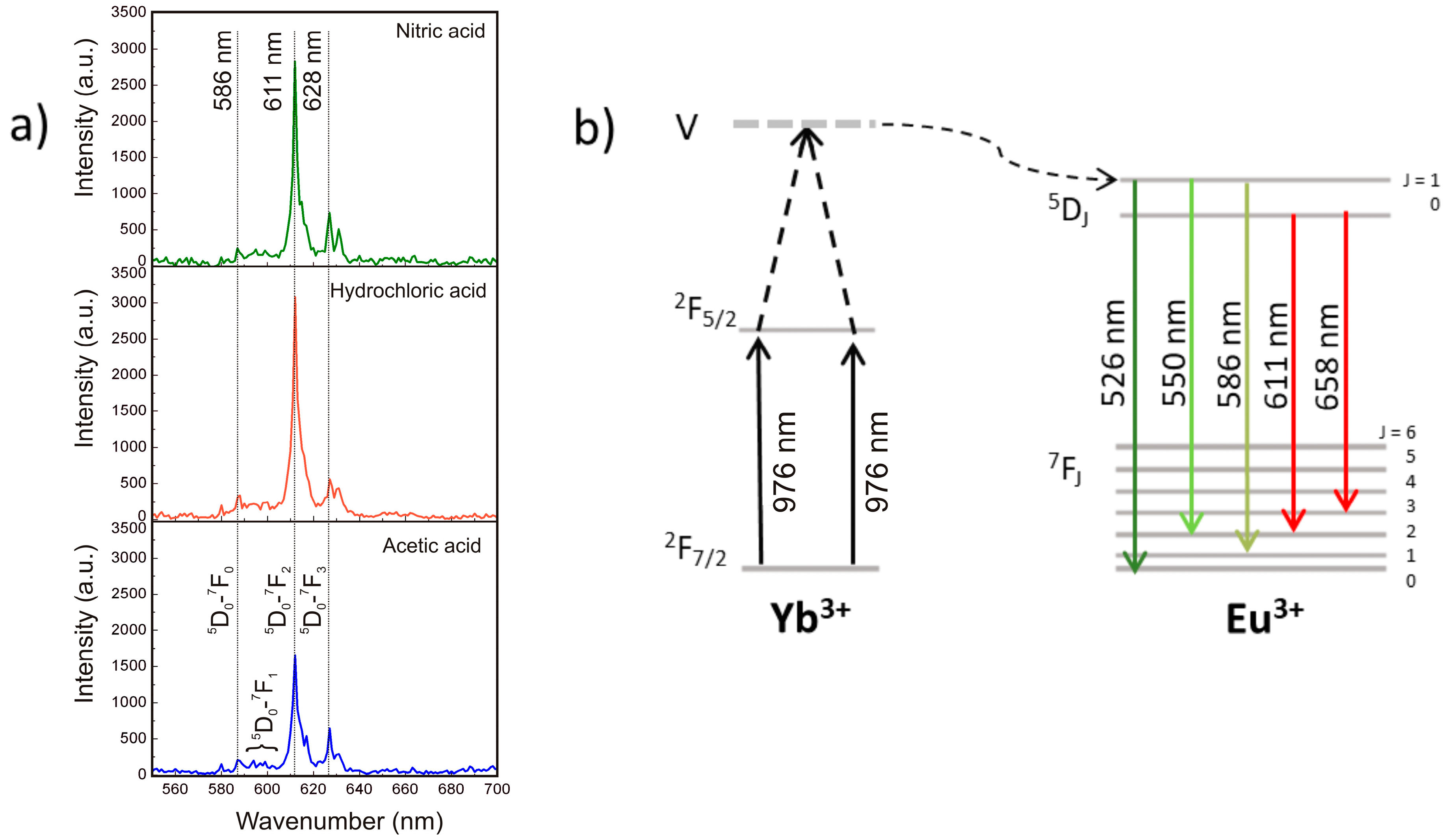
3.2. Optical Characterizations

The optical band gaps of Yb/Eu doped Y2O3 nanostructures were evaluated from diffuse reflectance data and through the Tauc relation using Equation (8):
( α h ν ) m = A ( h ν E g )
where α is the absorption coefficient, hν is the energy of photons impinging on the material, A is a constant of proportionality function of the matrix density of states and Eg is the optical band gap [54]. For such materials, it has been reported that they exhibit a direct allowed transition [55]. Few studies reported the optical band gaps for analogous materials, nevertheless Halappa et al. [55] described Eu3+ activated Y2O3 red nanophosphors with a band gap of 5.51 eV. In another study, Shivaramu et al. [56] demonstrated a band gap value of 5.7 eV also to Y2O3:Eu3+ nanophosphors. In the present study, the band gap values calculated were 4.56 eV, 4.36 eV and 4.53 eV for the materials produced with acetic, hydrochloric and nitric acids, respectively (Figure 9). The values are expressively low, when compared to the literature; however, it is known that adding dopants into the Y2O3 lattice causes energy levels in the energy gap between the conduction and valence bands (energy levels of donors or acceptors), which will lead to the decrease of the optical band gap [57]. In fact, Cabello-Guzmán et. al. [57] reported the progressive decrease of optical band gap by having two (Y2O3:Er –5.02 eV) or three dopants (Y2O3:Er-Yb –4.78 eV) in the host matrix. Moreover, it is expected that material defects and oxygen vacancies can also form discrete energy levels, influencing so the nanostructure’s band gaps. The band gap differences observed between the materials can also be justified by the size and structure disparities observed.
No direct relation between the nanostructure sizes measured by SEM/STEM and the band gaps values can be stated, however, considering the XRD results (Figure 4), a trend can be inferred, since the lower crystalline size material achieved the highest band gap value (acetate-based material), while the hydrochloric material revealed the lowest band gap value and displayed the highest crystallite size. It is normally accepted that the band gap is strongly dependent on crystallite size [58,59,60], and that the decrease in the band gap can be related to the increase in the grain size [58]. Moreover, other factors such as the degree of compactness and densification can also contribute to the final band gap value [61].
Figure 10 shows the emission spectra of the Yb3+:Eu3+ doped Y2O3 nanostructures prepared with different acids and a schematic of the relevant luminescence transitions between the 5D0 and the 7FJ states [44,62]. The produced materials exhibited a strong red emission under excitation with a 976 nm laser. Nevertheless, it is known that the Eu3+ ions cannot be excited with an excitation source around 980 nm due to a considerable mismatch of energy levels in Eu3+ ions. However, when co-doped with Yb3+, the upconversion emission occurs, indicating that the Eu3+ ions are excited with the Yb3+ ions [2,63].
When exposed to a 976 nm source, pairs of Yb3+ ions are excited from its 2F7/2 ground state to the 2F5/2. Then, their energy is transferred cooperatively in a way that one of them (acceptor) after gaining energy from the donor, occupies the virtual state (V) (i.e., 2F5/2 + 2F5/2 → 22F5/2). At this point, the excited Yb3+ ions from the virtual state transfer their excitation energy into the ground state of Eu3+ ions. Therefore, the Eu3+ ion is assumed to transit to the 5D2 multiplet term or to the 5D1 multiplet, followed by a nonradiative decay of the 5D0, and thus by emission [2,63].
The emission spectra observed in Figure 10 revealed radiative emissions at ~586 nm, 611 nm, and 628 nm, for all the materials produced. The emission bands can be assigned to the 5D07FJ (J = 0, 1, 2) transitions of Eu3+ [63]. The strongest peak at 611 nm is originated from 5D0 to 7F2 transition. When comparing between the material’s emission intensities, it can be observed that the emission bands are sharpen for the hydrochloric and nitric acid-based materials (the maximum values for the 5D07F2 transitions were 3050 and 2840, for hydrochloric and nitric acid-based materials, respectively). The lower emission observed for the acetic-based material (maximum value of 1650 for the 5D07F2 transition) can be associated to a size effect, since the luminescent intensity is known to be inversely proportional to the particle size, and thus the larger sized nanosheets are expected to have lower luminescence. Nevertheless, several aspects may influence the relative emission intensities of all materials, including absorption cross-section, competition between radiative cooperative emission, energy transfer to Eu3+ and energy migration to traps [63], besides a mesoscopic effect, associated to the shape and configuration of the nanostructures produced.

4. Conclusions

The fast microwave syntheses (15 min) of Yb/Eu doped Y2O3 nanostructures was reported. Microwave syntheses revealed itself to be an efficient way for successfully doping the Y2O3 host matrix after dissociating the primary oxides with different acids. In fact, this study revealed the key role of the acids used regarding the final structure and optical behaviour of the nanostructures produced. SEM and STEM revealed that the acetic acid resulted in nanosheets, while both hydrochloric and nitric formed nanospheres with heterogeneities in size. The study indicated the calcination temperature (700 °C) at which the conversion into Y2O3 is complete for such nanostructures. This temperature range is expected to cause an impact on production and energy costs of such nanostructures—in fact the calcination temperature is substantially lower than what is usually reported in literature. The optical properties of the produced materials were discussed, and the photoluminescence experiments showed a red Eu3+ emission when exited to a 976 nm source. Moreover, the sphere-like structures revealed enhanced luminescence, when compared to the nanosheets. The lower emission of the nanosheets was associated to a size effect, since acetic acid originated larger structures. The present study opens up to the possibility of these materials to be used as infrared to visible upconverters, and their potential to be integrated in several opto-electronic devices. For further studies, it is imperative to control the particle size and the size distribution of the developed nanostructures, which can be achieved by altering the catalyst or its concentration, but also with further investigation and adjustments on the synthesis parameters.

Author Contributions

D.N. and A.P. were responsible for writing the original manuscript with equal contribution; M.M. and T.F. performed the experiments; optical characterization was performed by A.P.; the DSC-TG and XRD characterization was performed by A.P.; D.N. performed the SEM; P.A.C. performed the STEM measurements; A.A., F.S., P.G. and S.G. participated in the review and editing and are responsible for funding, and finally the paper was under the supervision of R.M. and E.F.

Funding

This work was supported by FEDER funds, through the COMPETE 2020 Program, and national funds, through the Fundação para Ciência e Tecnologia (FCT), under the projects POCI-01-0145-FEDER-007688 (Reference UID/CTM/50025). The authors also acknowledge funding from the European Commission through the projects 1D-NEON (H2020-NMP-2015, grant 685758-21D) and BET-EU (H2020-TWINN-2015, grant 692373. The work was also partially funded by the Nanomark collaborative project between INCM (Imprensa Nacional—Casa da Moeda) and CENIMAT/i3N. D. Nunes and A. Pimentel acknowledge funding from FCT through the grants SFRH/BPD/84215/2012 and SFRH/BPD/76992/2011, respectively. P.A. Carvalho acknowledges support from the Research Council of Norway through grants 275752 and 197405/F50.

Conflicts of Interest

The authors declare no conflicts of interest.

References

  1. De Wild, J.; Meijerink, A.; Rath, J.K.; Van Sark, W.G.J.H.M.; Schropp, R.E.I. Upconverter solar cells: Materials and applications. Energy Environ. Sci. 2011, 4, 4835–4848. [Google Scholar] [CrossRef]
  2. Pandey, A. Sensitization Effect of Yb3+ in Upconversion Luminescence of Eu3+Codoped Y2O3 Phosphor. J. Phys. Chem. Biophys. 2013, 3, 1–3. [Google Scholar] [CrossRef]
  3. Nazarov, M.; Noh, D.Y. Rare earth double activated phosphors for different applications. J. Rare Earths 2010, 28, 1–11. [Google Scholar] [CrossRef]
  4. Atwood, D.A. The Rare Earth Elements: Fundamentals and Application; John Wiley & Sons: New York, NY, USA, 2006. [Google Scholar] [CrossRef]
  5. Bünzli, J.C.G.; Eliseeva, S.V. Lanthanide NIR luminescence for telecommunications, bioanalyses and solar energy conversion. J. Rare Earths 2010, 28, 824–842. [Google Scholar] [CrossRef]
  6. Bünzli, J.-C.G.; Eliseeva, S.V. Basics of Lanthanide Photophysics. Lanthan. Lumin. 2010, 7, 1–45. [Google Scholar] [CrossRef]
  7. Bedekar, V.; Dutta, D.P.; Mohapatra, M.; Godbole, S.V.; Ghildiyal, R.; Tyagi, A.K. Rare-earth doped gadolinia based phosphors for potential multicolor and white light emitting deep UV LEDs. Nanotechnology 2009, 20, 125707. [Google Scholar] [CrossRef] [PubMed]
  8. Guo, C.; Huang, D.; Su, Q. Methods to improve the fluorescence intensity of CaS:Eu2+ red-emitting phosphor for white LED. Mater. Sci. Eng. B 2006, 130, 189–193. [Google Scholar] [CrossRef]
  9. Ballato, J.; Lewis, J.S.; Holloway, P. Display Applications of Rare-Earth-Doped Materials. MRS Bull. 1999, 24, 51–56. [Google Scholar] [CrossRef]
  10. Leskelä, M.; Niinistö, L. Applications of rare earths in full-colour EL displays. Mater. Chem. Phys. 1992, 31, 7–11. [Google Scholar] [CrossRef]
  11. Kenyon, A. Recent developments in rare-earth doped materials for optoelectronics. Prog. Quantum Electron. 2002, 26, 225–284. [Google Scholar] [CrossRef]
  12. Optical Sensor Utilizing Rare-Earth-Doped Integrated-Optic Lasers. 1995. Available online: https://patents.google.com/patent/US5677769A/en (accessed on 28 November 2018).
  13. Steckl, A.J.; Zavada, J.M. Photonic Applications of Rare-Earth-Doped Materials. MRS Bull. 1999, 24, 16–20. [Google Scholar] [CrossRef]
  14. Rare Earth Doped and Large Effective Area Optical Fibers for Fiber Lasers and Amplifiers. 2010. Available online: https://patents.google.com/patent/US8213758B2/en (accessed on 28 November 2018).
  15. Seddon, A.B.; Tang, Z.; Furniss, D.; Sujecki, S.; Benson, T.M. Progress in rare-earth-doped mid-infrared fiber lasers. Opt. Express 2010, 18, 26704. [Google Scholar] [CrossRef] [PubMed]
  16. Zhou, X.; Huang, Y.; Liu, C.; Liao, J.; Lu, T.; Xing, W. Available hydrogen from formic acid decomposed by rare earth elements promoted Pd-Au/C catalysts at low temperature. ChemSusChem 2010, 3, 1379–1382. [Google Scholar] [CrossRef] [PubMed]
  17. Yu, L.; Lu, Y.; Man, N.; Yu, S.-H.; Wen, L.-P. Rare Earth Oxide Nanocrystals Induce Autophagy in HeLa Cells. Small 2009, 5, 2784–2787. [Google Scholar] [CrossRef] [PubMed]
  18. Xu, C.; Qu, X. Cerium oxide nanoparticle: A remarkably versatile rare earth nanomaterial for biological applications. NPG Asia Mater. 2014, 6, e90. [Google Scholar] [CrossRef]
  19. Shalav, A.; Richards, B.S.; Green, M.A. Luminescent layers for enhanced silicon solar cell performance: Up-conversion. Sol. Energy Mater. Sol. Cells 2007, 91, 829–842. [Google Scholar] [CrossRef]
  20. Vicente, A.T.; Araújo, A.; Mendes, M.J.; Nunes, D.; Oliveira, M.J.; Sanchez-Sobrado, O.; Ferreira, M.P.; Águas, H.; Fortunato, E.; Martins, R. Multifunctional cellulose-paper for light harvesting and smart sensing applications. J. Mater. Chem. C 2018, 6, 3143–3181. [Google Scholar] [CrossRef]
  21. Hu, S.; Zhang, H.; Yang, J.; Qiao, Z. Hydrothermal Synthesis and Green Luminescent Properties of Lu2O3:Yb3+/Ho3+ Nanocubes. J. Nanosci. Nanotechnol. 2014, 14, 3853–3860. [Google Scholar] [CrossRef]
  22. Jones, S.L.; Kumar, D.; Singh, R.K.; Holloway, P.H. Luminescence of pulsed laser deposited Eu doped yttrium oxide films. Appl. Phys. Lett. 1998, 71, 404. [Google Scholar] [CrossRef]
  23. Hao, J.; Studenikin, S.A.; Cocivera, M. Blue, green and red cathodoluminescence of Y2O3 phosphor films prepared by spray pyrolysis. J. Lumin. 2001, 93, 313–319. [Google Scholar] [CrossRef]
  24. Chen, K.; Peng, J.; Srinivasakannan, C.; Yin, S.; Guo, S.; Zhang, L. Effect of temperature on the preparation of yttrium oxide in microwave field. J. Alloys Compd. 2018, 742, 13–19. [Google Scholar] [CrossRef]
  25. Mangalaraja, R.V.; Mouzon, J.; Hedström, P.; Camurri, C.P.; Ananthakumar, S.; Odén, M. Microwave assisted combustion synthesis of nanocrystalline yttria and its powder characteristics. Powder Technol. 2009, 191, 309–314. [Google Scholar] [CrossRef]
  26. Agrawal, S.; Dubey, V. Down conversion luminescence behavior of Er and Yb doped Y2O3 phosphor. J. Radiat. Res. Appl. Sci. 2014, 7, 601–606. [Google Scholar] [CrossRef]
  27. Mishra, K.C.; Berkowitz, J.K.; Johnson, K.H.; Schmidt, P.C. Electronic structure and optical properties of europium-activated yttrium oxide phosphor. Phys. Rev. B 1992, 45, 10902–10906. [Google Scholar] [CrossRef]
  28. Chávez, D.H.; Contreras, O.E.; Hirata, G.A. Synthesis and Upconversion Luminescence of Nanoparticles Y2O3 and Gd2O3 Co-doped with Yb3+ and Er3+. Nanomater. Nanotechnol. 2016, 6, 7. [Google Scholar] [CrossRef]
  29. Yang, J.; Gu, J.; Yang, R.; Shang, Q.; Yang, J. Hydrothermal Synthesis Y2O3:Yb3+/Er3+ Nanospheres with Upconversion Luminescence from Green to Red. Nanosci. Nanometrol. 2016, 2, 41–45. [Google Scholar] [CrossRef]
  30. Dhanaraj, J.; Jagannathan, R.; Kutty, T.R.N.; Lu, C.-H. Photoluminescence Characteristics of Y2O3:Eu3+ Nanophosphors Prepared Using Sol−Gel Thermolysis. J. Phys. Chem. B 2001, 105, 11098–11105. [Google Scholar] [CrossRef]
  31. Zhai, Y.; Yao, Z.; Ding, S.; Qiu, M.; Zhai, J. Synthesis and characterization of Y2O3:Eu nanopowder via EDTA complexing sol–gel process. Mater. Lett. 2003, 57, 2901–2906. [Google Scholar] [CrossRef]
  32. Lakshminarasappa, B.N.; Jayaramaiah, J.R.; Nagabhushana, B.M. Thermoluminescence of combustion synthesized yttrium oxide. Powder Technol. 2012, 217, 7–10. [Google Scholar] [CrossRef]
  33. Capobianco, J.A.; Vetrone, F.; D’Alesio, T.; Tessari, G.; Speghini, A.; Bettinelli, M. Optical spectroscopy of nanocrystalline cubic Y2O3:Er3+ obtained by combustion synthesis. Phys. Chem. Chem. Phys. 2000, 2, 3203–3207. [Google Scholar] [CrossRef]
  34. Chen, J.; Huang, B.; Huang, C.; Sun, X. Preparation of nanoscaled yttrium oxide by citrate precipitation method. J. Rare Earths 2017, 35, 79–84. [Google Scholar] [CrossRef]
  35. Jeong, J.Y.; Park, S.W.; Moon, D.K.; Kim, W.J. Synthesis of Y2O3 nano-powders by precipitation method using various precipitants and preparation of high stability dispersion for backlight unit (BLU). J. Ind. Eng. Chem. 2010, 16, 243–250. [Google Scholar] [CrossRef]
  36. Tian, Y.; Lu, F.; Xing, M.; Ran, J.; Fu, Y.; Peng, Y.; Luo, X. Upconversion luminescence properties of Y2O2S:Er3+@Y2O2S:Yb3+, Tm3+ core-shell nanoparticles prepared via homogeneous co-precipitation. Opt. Mater. (Amst.) 2017, 64, 58–63. [Google Scholar] [CrossRef]
  37. Khachatourian, A.M.; Golestani-Fard, F.; Sarpoolaky, H.; Vogt, C.; Vasileva, E.; Mensi, M.; Popov, S.; Toprak, M.S. Microwave synthesis of Y2O3:Eu3+ nanophosphors: A study on the influence of dopant concentration and calcination temperature on structural and photoluminescence properties. J. Lumin. 2016, 169, 1–8. [Google Scholar] [CrossRef]
  38. Malek Khachatourian, A.; Golestani-Fard, F.; Sarpoolaky, H.; Vogt, C.; Toprak, M.S. Microwave assisted synthesis of monodispersed Y2O3 and Y2O3:Eu3+ particles. Ceram. Int. 2015, 41, 2006–2014. [Google Scholar] [CrossRef]
  39. Pimentel, A.; Samouco, A.; Nunes, D.; Araújo, A.; Martins, R.; Fortunato, E. Ultra-fast microwave synthesis of ZnO nanorods on cellulose substrates for UV sensor applications. Materials (Basel) 2017, 10, 1308. [Google Scholar] [CrossRef]
  40. Pimentel, A.; Nunes, D.; Pereira, S.; Martins, R.; Fortunato, E. Photocatalytic Activity of TiO2 nanostructured arrays prepared by microwave-assisted solvothermal method. In Semiconductor Photocatalysis—Materials, Mechanisms and Applications; Cao, W., Ed.; InTech: Rijeka, Croatia, 2016. [Google Scholar] [CrossRef]
  41. Nunes, D.; Pimentel, A.; Barquinha, P.; Carvalho, P.A.; Fortunato, E.; Martins, R. Cu2O polyhedral nanowires produced by microwave irradiation. J. Mater. Chem. C 2014, 2, 6097. [Google Scholar] [CrossRef]
  42. Anh, T.; Benalloul, P.; Barthou, C.; Giang, L.T.; Vu, N.; Minh, L. Luminescence, energy transfer, and upconversion mechanisms of Y2O3 nanomaterials doped with Eu3+, Tb3+, Tm3+, Er3+, and Yb3+ ions. J. Nanomater. 2007, 2007, 1–10. [Google Scholar] [CrossRef]
  43. Sordelet, D.; Akinc, M. Preparation of spherical, monosized Y2O3 precursor particles. J. Colloid Interface Sci. 1988, 122, 47–59. [Google Scholar] [CrossRef]
  44. Jia, G.; Yang, M.; Song, Y.; You, H.; Zhang, H. General and Facile Method To Prepare Uniform Y2O3:Eu Hollow Microspheres. Cryst. Growth Des. 2009, 9, 301–307. [Google Scholar] [CrossRef]
  45. Sung, J.M.; Lin, S.E.; Wei, W.C.J. Synthesis and reaction kinetics for monodispersive Y2O3:Tb3+ spherical phosphor particles. J. Eur. Ceram. Soc. 2007, 27, 2605–2611. [Google Scholar] [CrossRef]
  46. Schneider, C.A.; Rasband, W.S.; Eliceiri, K.W. NIH Image to ImageJ: 25 years of image analysis. Nat. Methods 2012, 9, 671–675. [Google Scholar] [CrossRef]
  47. Byrappa, K.; Yoshimura, M. Handbook of Hydrothermal Technology—A Technology for Crystal Growth and Materials Processing; Noyes Publication: Norwich, NY, USA, 2001. [Google Scholar]
  48. Balabanov, S.S.; Gavrishchuk, E.M.; Permin, D.A. Synthesis and properties of yttrium hydroxyacetate sols. Inorg. Mater. 2012, 48, 500–503. [Google Scholar] [CrossRef]
  49. Lojpur, V.; Nikolic, M.; Mancic, L.; Milosevic, O.; Dramicanin, M.D. Y2O3:Yb,Tm and Y2O3:Yb,Ho powders for low-temperature thermometry based on up-conversion fluorescence. Ceram. Int. 2013, 39, 1129–1134. [Google Scholar] [CrossRef]
  50. Wang, H.; Uehara, M.; Nakamura, H.; Miyazaki, M.; Maeda, H. Synthesis of well-dispersed Y2O3:Eu nanocrystals and self-assembled nanodisks using a simple non-hydrolytic route. Adv. Mater. 2005, 17, 2506–2509. [Google Scholar] [CrossRef]
  51. Sarpoolaky, H.; Fard, F.G.; Khachatourian, A.M. Ceramics International Microwave Assisted Synthesis of Monodispersed Y2O3 and Y2O3:Eu3þ Particles. Available online: http://www.academia.edu/36133797/CERAMICS_INTERNATIONAL_Microwave_assisted_synthesis_of_monodispersed_Y_2_O_3_and_Y_2_O_3_Eu_3_þ_particles (accessed on 22 December 2018).
  52. Liu, W.; Wang, Y.; Zhang, M.; Zheng, Y. Synthesis of Y2O3:Eu3+ coated Y2O3 phosphors by urea-assisted homogeneous precipitation and its photoluminescence properties. Mater. Lett. 2013, 96, 42–44. [Google Scholar] [CrossRef]
  53. Custelcean, R. Crystal engineering with urea and thiourea hydrogen-bonding groups. Chem. Commun. 2008, 3, 295–307. [Google Scholar] [CrossRef]
  54. Tauc, J. Optical properties and electronic structure of amorphous Ge and Si. Mater. Res. Bull. 1968, 3, 37–46. [Google Scholar] [CrossRef]
  55. Halappa, P.; Raj, S.T.; Sairani, R.; Joshi, S.; Madhusudhana, R.; Shivakumara, C. Combustion synthesis and characterisation of Eu3+-activated Y2O3 red nanophosphors for display device applications. Int. J. Nanotechnol. 2017, 14, 833–844. [Google Scholar] [CrossRef]
  56. Shivaramu, N.J.; Lakshminarasappa, B.N.; Nagabhushana, K.R.; Singh, F.; Swart, H.C. Synthesis, thermoluminescence and defect centres in Eu3+ doped Y2O3 nanophosphor for gamma dosimetry applications. Mater. Res. Express 2017, 4, 115033. [Google Scholar] [CrossRef]
  57. Cabello-Guzmán, G.; González, D.; Caro-Díaz, C.; Lillo-Arroyo, L.; Valenzuela-Melgarejo, F.; Cárdenas Triviño, G.; Buono-Core, G.E.; Chornik, B.; Huentupil, Y. Preliminary evaluation of the up-conversion emission of Y2O3:Er-Yb thin films prepared by a solid state photochemical deposition method. J. Lumin. 2018, 204, 401–409. [Google Scholar] [CrossRef]
  58. Ramana, C.V.; Smith, R.J.; Hussain, O.M. Grain size effects on the optical characteristics of pulsed-laser deposited vanadium oxide thin films. Phys. Status Solidi 2003, 199, R4–R6. [Google Scholar] [CrossRef]
  59. Migas, D.B.; Filonov, A.B.; Borisenko, V.E.; Skorodumova, N.V. Orientation effects in morphology and electronic properties of anatase TiO2 one-dimensional nanostructures. II. Nanotubes. Phys. Chem. Chem. Phys. 2014, 16, 9490–9498. [Google Scholar] [CrossRef] [PubMed]
  60. Nunes, D.; Pimentel, A.; Pinto, J.V.; Calmeiro, T.R.; Nandy, S.; Barquinha, P.; Pereira, L.; Carvalho, P.A.; Fortunato, E.; Martins, R. Photocatalytic behavior of TiO2 films synthesized by microwave irradiation. Catal. Today 2016, 278, 262–270. [Google Scholar] [CrossRef]
  61. Pereira, L.; Barquinha, P.; Fortunato, E.; Martins, R.; Kang, D.; Kim, C.J.; Lim, H.; Song, I.; Park, Y. High k dielectrics for low temperature electronics. Thin Solid Films 2008, 516, 1544–1548. [Google Scholar] [CrossRef]
  62. Xiao, Y.; Han, G.; Chang, Y. Electrospun ytterbium and europium ions co-doped stannic oxide nanofibers and application in dye-sensitized solar cells. Mater. Res. Bull. 2017, 92, 90–98. [Google Scholar] [CrossRef]
  63. Wang, H.; Duan, C.K.; Tanner, P.A. Visible upconversion luminescence from Y2O3:Eu3+,Yb3+. J. Phys. Chem. C 2008, 112, 16651–16654. [Google Scholar] [CrossRef]
Figure 1. Schematic of Yb/Eu doped Y2O3 nanostructures produced by a hydrothermal process under microwave irradiation.
Nanomaterials 09 00234 g001
Figure 2. X-Ray diffraction (XRD) diffractograms of nanostructures after microwave synthesis and before any calcination, for the three sets of reactions defined above.
Nanomaterials 09 00234 g002
Figure 3. In situ XRD diffractograms as a function of temperature (on top) and the respective contour plot (on bottom) of Yb/Eu doped Y2O3 nanostructures after microwave synthesis, when using (a) acetic, (b) hydrochloric and (c) nitric acids.
Nanomaterials 09 00234 g003
Figure 4. XRD diffractograms of Yb/Eu doped Y2O3 nanostructures after calcination at 700 °C. The simulated Y2O3 powder pattern is also shown for comparison.
Nanomaterials 09 00234 g004
Figure 5. Thermogravimetric analysis and differential scanning calorimetry (TGA/DSC) curves of the as-synthesized nanostructures before calcination produced with (a) acetic acid, (b) hydrochloric acid and (c) nitric acid.
Nanomaterials 09 00234 g005
Figure 6. Scanning electron microscopy (SEM) images of Yb/Eu doped Y2O3 nanostructures produced by hydrothermal method assisted by microwave radiation, and using (a,b) acetic acid, (c,d) hydrochloric acid and (e,f) nitric acid, before and after annealing at 700 °C, respectively. The insets magnify the structures produced after calcination.
Nanomaterials 09 00234 g006
Figure 7. Scanning transmission electron microscopy (STEM) images of Y2O3:Yb:Eu nanostructures produced by hydrothermal method assisted by microwave irradiation, and using (a,d) acetic acid, (b,e) hydrochloric acid, and (c,f) nitric acid after calcination at 700 °C.
Nanomaterials 09 00234 g007
Figure 8. STEM images (a,f) and energy dispersive X-Ray spectroscopy (EDS) analyses of the Yb/Eu doped Y2O3 nanostructures after microwave synthesis and calcination at 700 °C. The corresponding EDS maps for Y (b,g), Yb (c,h), Eu (d,i), and O (e,j) are presented. The two types of structures have been analyzed.
Nanomaterials 09 00234 g008
Figure 9. Tauc plot for the Yb/Eu doped Y2O3 nanostructures produced with acetic, hydrochloric and nitric acids, respectively.
Nanomaterials 09 00234 g009
Figure 10. (a) Emission spectra of the Yb/Eu doped Y2O3 nanostructures obtained at 976 nm, and (b) Energy level diagram for Yb3+ and Eu3+ together with the relevant luminescence transitions between the 5D0 and the 7FJ states.
Nanomaterials 09 00234 g010
Table 1. Transitions of lanthanide elements [3,4,5,6].
ElementColor of the Visible LuminescenceTransitionIntensity
Ce, ceriumUV5d → 2F5/2 (300–450 nm)n.a.
Pr, praseodymiumRed1D24H4 (600 nm)
3P03F2 (700 nm)
Weak
Nd, neodymiumInfra-red4F3/24I9/2 (900 nm)n.a.
Sm, samariumOrange–red4G5/26H7/2 (600 nm)Medium
Eu, europiumRed–orange5D07F4 (720 nm)
5D07F3 (650 nm)
5D07F2 (615 nm)
5D07F1 (590 nm)
5D07F0 (580 nm)
Strong
Gd, gadoliniumUV6P7/28S7/2 (310 nm)Strong
Td, terbiumGreen–orange5D47F5 (540 nm)
5D47F4 (580 nm)
5D47F3 (620 nm)
5D47F2 (650 nm)
5D47F1 (660 nm)
Strong
Dy, dysprosiumYellow4F9/26H13/2 (570 nm)
4I15/26H13/2 (540 nm)
Medium
Ho, holmiumRed5F55I8 (650 nm)Weak
Er, erbiumGreen4S3/24I15/2 (545 nm)
4F9/24I15/2 (660 nm)
Weak
Tm, thuliumBlue1G43H6 (470 nm)Weak
Yb, ytterbiumInfra-red2F5/27F7/2 (980 nm)n.a.
n.a.—not available.

