Heteroepitaxial Growth of T-Nb2O5 on SrTiO3


Leibniz-Institut für Kristallzüchtung, Max-Born-Straße 2, D-12489 Berlin, Germany
*
Author to whom correspondence should be addressed.
Nanomaterials 2018, 8(11), 895; https://doi.org/10.3390/nano8110895
Submission received: 15 October 2018
/
Revised: 29 October 2018
/
Accepted: 30 October 2018
/
Published: 1 November 2018
Abstract
:There is a growing interest in exploiting the functional properties of niobium oxides in general and of the T-Nb2O5 polymorph in particular. Fundamental investigations of the properties of niobium oxides are, however, hindered by the availability of materials with sufficient structural perfection. It is expected that high-quality T-Nb2O5 can be made using heteroepitaxial growth. Here, we investigated the epitaxial growth of T-Nb2O5 on a prototype perovskite oxide, SrTiO3. Even though there exists a reasonable lattice mismatch in one crystallographic direction, these materials have a significant difference in crystal structure: SrTiO3 is cubic, whereas T-Nb2O5 is orthorhombic. It is found that this difference in symmetry results in the formation of domains that have the T-Nb2O5 c-axis aligned with the SrTiO3 <001>s in-plane directions. Hence, the number of domain orientations is four and two for the growth on (100)s- and (110)s-oriented substrates, respectively. Interestingly, the out-of-plane growth direction remains the same for both substrate orientations, suggesting a weak interfacial coupling between the two materials. Despite challenges associated with the heteroepitaxial growth of T-Nb2O5, the T-Nb2O5 films presented in this paper are a significant improvement in terms of structural quality compared to their polycrystalline counterparts.
1. Introduction
Niobium oxides have been studied for a long time [1,2] and are of technological interest for different potential applications. For example, niobium oxides are very attractive for energy storage applications due to their intercalation pseudocapacitance [3,4]. In addition, niobium oxides can be used as selectors or data storage elements in future nonvolatile memory applications [5,6]. The most thermodynamically stable niobium oxide is niobium pentoxide (Nb2O5) [1,2]. Nb2O5 has many different polymorphs that are discussed elsewhere in detail [1,2]. The most important polymorphs are the low-temperature polymorph, T-Nb2O5, which has an orthorhombic symmetry with a superstructure [7], and the high-temperature polymorph, H-Nb2O5, which is the most stable polymorph and has a monoclinic symmetry [8]. Of these two, T-Nb2O5 is the most relevant for practical applications, because it can be formed at lower temperatures and exhibits intercalation pseudocapacitance [3,4]. Unfortunately, the availability of niobium oxides with high structural perfection, such as bulk single crystals or as a single-crystal layer, is limited, to date. This makes it difficult to determine the fundamental functional properties of niobium oxides, such as anisotropic optical constants, energetic levels of relevant point defects, or anisotropies in electrical conduction. The determination of these properties is highly desirable in order to improve the functionality of niobium oxides for applications.
Heteroepitaxial film growth is interesting in this respect, because it enables the fabrication of high-quality material on foreign substrates and the determination of its properties. Even though polycrystalline T-Nb2O5 films are well studied (see, for example, References [9,10]), epitaxial T-Nb2O5 thin films are not widely available nor studied. Hence, for the full exploitation of their functional properties, the growth of epitaxial T-Nb2O5 is urgently needed.
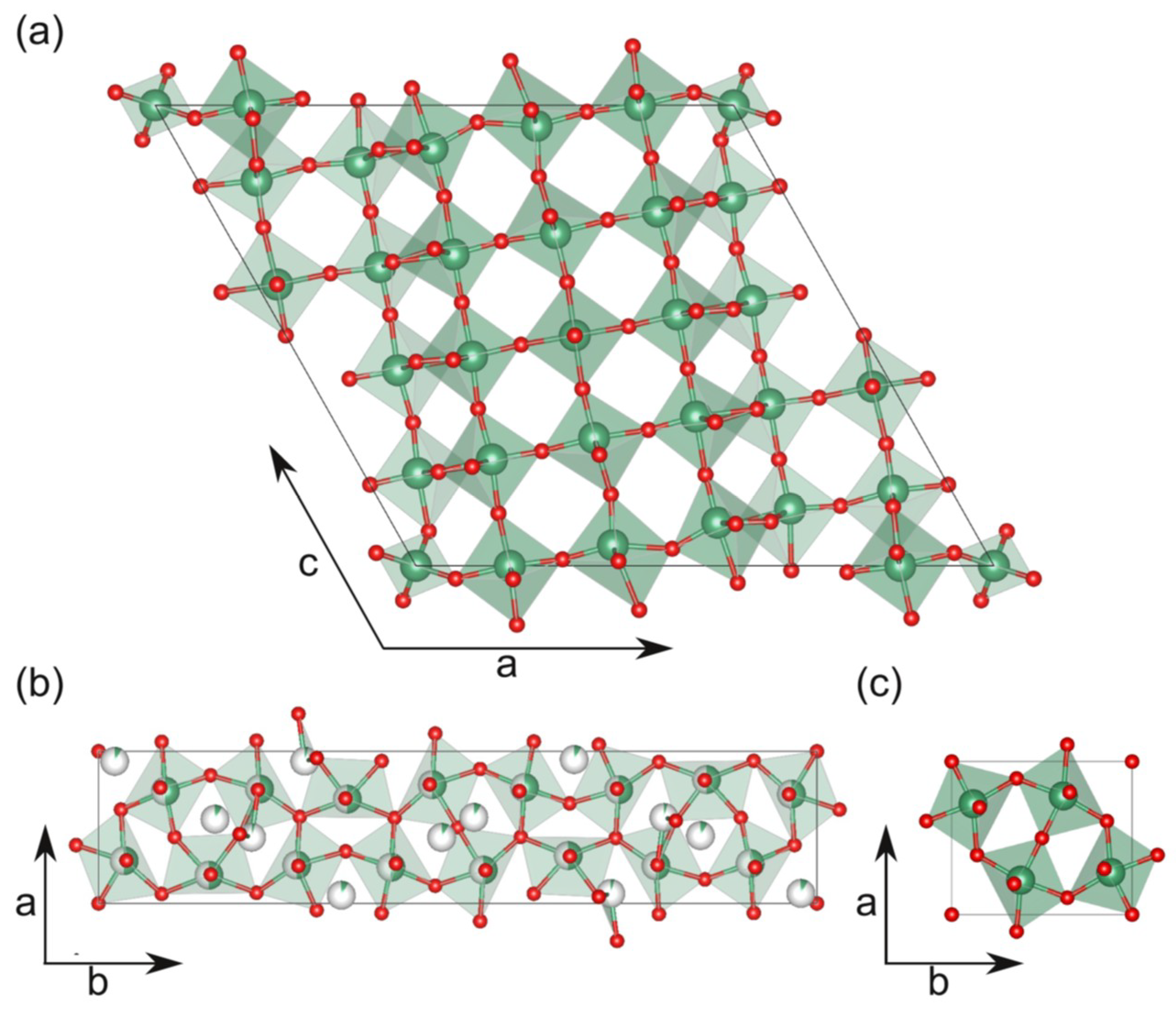
Both the T-Nb2O5 and the H-Nb2O5 polymorphs consist of oxygen octahedra that are connected by their corners, as well as by their edges, as seen in Figure 1b,c and Figure 1a, respectively. For T-Nb2O5, the structure determined by Kato et al. [11] is shown in Figure 1b, whereas a simplified model of T-Nb2O5 based on Lee et al. [12] is shown in Figure 1c. These configurations result in nanometer-sized unit cells with orthorhombic and monoclinic symmetry, respectively. Due to the unique symmetries of these polymorphs, no symmetry-matched substrate is available for heteroepitaxy. Advantageously, the lattice parameter of SrTiO3 (a = 3.905 Å) is well matched with the c-lattice parameter of T-Nb2O5 (3.938 Å) and b-lattice parameter of H-Nb2O5 (3.824 Å), resulting in lattice mismatches of −0.8% and +2.1%, respectively. Presently, it is unclear how the presence of this symmetry mismatch in combination with a good lattice match affects the growth and the structural properties of T-Nb2O5 thin films on SrTiO3. In order to investigate this, we have grown epitaxial Nb2O5 thin films on SrTiO3 using metal-organic chemical vapor deposition (MOCVD). First, the deposition regimes for the growth of T-Nb2O5 and H-Nb2O5 were identified. Next, we focused on the influence of the symmetry mismatch between T-Nb2O5 and SrTiO3 on the domain formation, because the T-Nb2O5 phase is the technologically most relevant phase. This influence was studied by employing (100)s- and (110)s-oriented SrTiO3 substrates. Finally, the microstructure of the T-Nb2O5 thin films was analyzed using transmission electron microscopy (TEM).
2. Materials and Methods
Thin films were grown by means of liquid-delivery spin metal-organic chemical vapor deposition (MOCVD). For the deposition, a 0.01 M or 0.005 M solution of niobium ethoxide (Nb(EtO)5) in toluene was used. The solution was evaporated in an evaporator with a temperature of 180 °C at a rate of approximately 0.45 mL/min. Using Ar as a carrier gas, the evaporated solution was fed into the MOCVD reactor. A rotation speed of the carrier of 750 rounds per minute was employed. Using a 0.01 M solution, a growth rate of approximately 1.5 nm/min was achieved. The (100)s SrTiO3 substrates were etched with buffered HF and subsequently annealed for 1 h at 1100 °C in a pure oxygen flow prior to the deposition. The (110)s SrTiO3 substrates were annealed for 1 h at 1000 °C in pure oxygen. The surface morphology of the substrates and films was studied using a Bruker Icon atomic force microscope (AFM, Billerica, MA, USA) operated in PeakForce Tapping® mode. The structural properties were studied by high-resolution X-ray diffraction (HRXRD) with a Bruker D8 Discover system (Billerica, MA, USA) using Cu Kα1 radiation. In order to differentiate between film and substrate, the indices film (“f”) and substrate (“s”) are added to the Miller indices of the film and substrate, respectively. The film thickness was determined by spectral ellipsometry using a Horiba Jobin Yvon MM-16 (Kyoto, Japan).
Cross-sectional transmission electron microscopy (TEM) investigations were performed with an aberration-corrected FEI Titan 80–300 (Hilsboro, OR, USA) operating at 300 kV. For high-resolution TEM (HRTEM) imaging, a spherical aberration of Cs = −10 µm was used, and all other aberrations were corrected to a minimum. TEM samples were prepared by mechanical polishing using diamond lapping foils down to a thickness of approximately 10 µm. Final thinning to electron transparency was done by argon ion milling, with accelerating voltages decreasing stepwise from 4 kV to 0.2 kV using a GATAN precision ion polishing system (PIPS, Pleasanton, CA, USA). The structural models presented in Figure 1and Figure 6 were made using VESTA [13].
3. Results and Discussion
3.1. Determination of the Growth Window
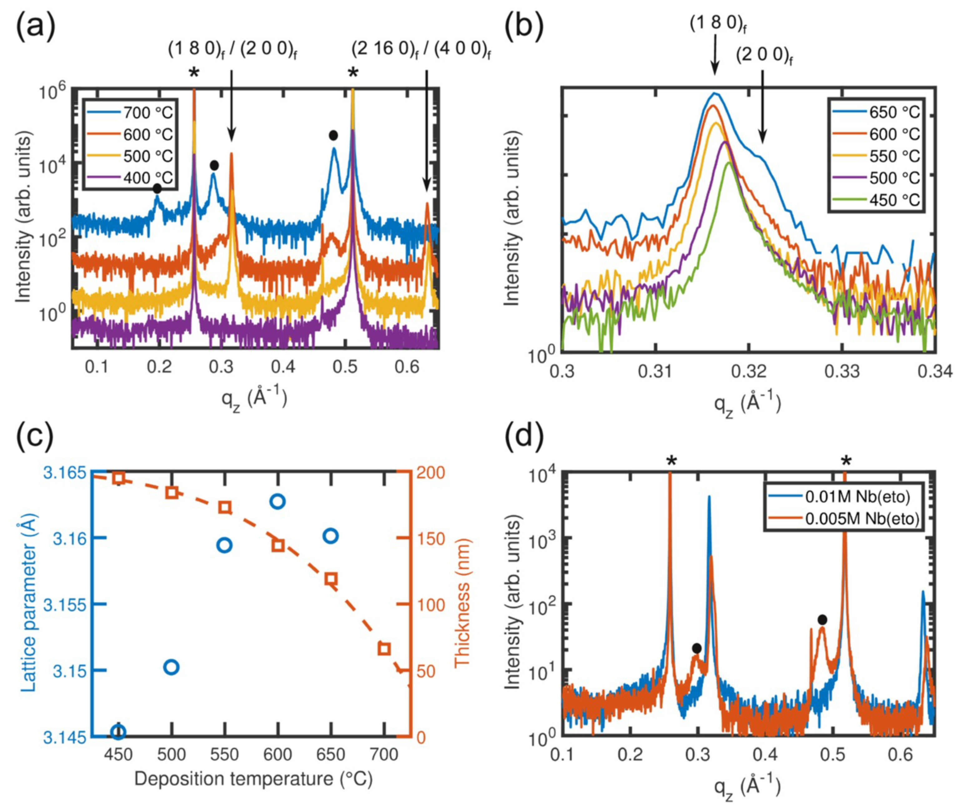
Initially, Nb2O5 films were grown on (100)s SrTiO3 substrates employing substrate temperatures between 400 °C and 750 °C with intervals of 50 °C in order to assess the growth window. Figure 2a shows the wide-range HRXRD profiles of films grown at temperatures of 400 °C, 500 °C, 600 °C, and 700 °C that capture the most important observations. All diffraction patterns contain sharp peaks at approximately 0.255 Å−1 and 0.51 Å−1 that belong to the (100)s and (200)s diffraction peaks of the SrTiO3 substrate, respectively (marked with an asterisk). The small peak observed at 0.46 Å−1 is a measurement artifact caused by Cu Kß radiation. The other Bragg peaks, which are visible in Figure 2a, are attributed to the niobium oxide films. Significant differences can be seen between the diffraction profiles of films grown at different temperatures.
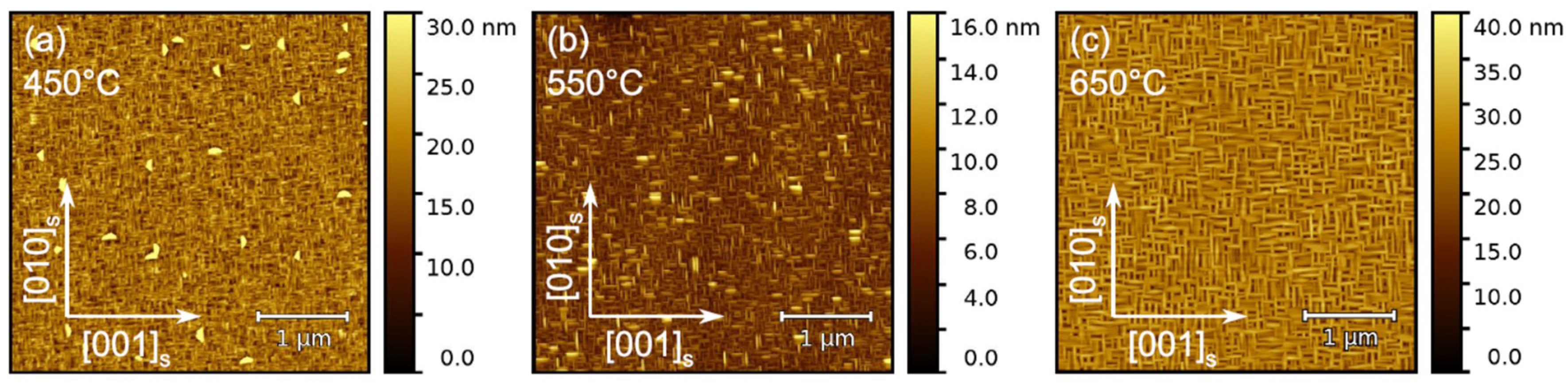
No diffraction peaks are observed for the film grown at 400 °C, indicating an amorphous film structure. With increasing substrate temperature, the occurrence of Bragg peaks indicates the formation of a crystalline phase. However, depending on temperature, differences in the diffraction pattern are visible: (1) The diffraction patterns of the films grown between 450 °C and 650 °C exhibit a strong peak at qz ≈ 0.316 Å−1 corresponding to a lattice spacing of about 3.165 Å. This spacing is in reasonable agreement with the (180)f lattice spacing of T-Nb2O5 (3.15 Å) [PDF 00-027-1313]. A higher magnification in the qz range between 0.3 Å−1 and 0.34 Å−1 (Figure 2b) shows that, additionally, a minor contribution at qz ≈ 0.322 Å−1 occurs that is attributed to the (200)f reflection of T-Nb2O5. The intensity of the (200)f reflection is approximately 1% of the (180)f diffraction peak for a deposition temperature of 600 °C and decreases with decreasing deposition temperature. The overall shift of the film peak to lower qz values with increasing deposition temperature indicates that the lattice parameter increases, as shown in Figure 2c. This might be simply explained by an increase in the build-up of compressive strain when cooling the sample to room temperature after growth that is induced by the difference in the thermal expansion coefficient between Nb2O5 (1.3 × 10⁻⁵ K−1 [14]) and the SrTiO3 substrate (3.23 × 10⁻⁵ K−1 [15]). AFM investigations (see Figure 3) show that on (100)s SrTiO3 substrates, T-Nb2O5 grows with a fourfold rotational symmetry with needle-like grains aligned along the [010]s and [001]s directions of the substrate (in the following, the indices “f” and “s” denote the film and the substrate directions, respectively). Moreover, it can be seen that the grain size increases with increasing growth temperature. Such a change in grain size can result in the development of a tensile strain in the thin film that originates during the grain boundary formation [16], which would result in a shift of the (180)f diffraction peak to higher qz values with increasing growth temperature. This is observed for temperatures above 600 °C, suggesting that both the difference in thermal expansion and the domain size contribute to the strain state of the T-Nb2O5 film.
For the film grown at 700 °C, the T-Nb2O5 (180)f and (200)f peaks in the HRXRD θ/2θ scan are no longer visible. Instead, three Bragg reflections at 0.197 Å−1, 0.287 Å−1, and 0.481 Å−1 (marked by black circles in Figure 2a) are observed. These three peaks belong to the (301)f, (402)f, and (703)f diffraction peaks of the high-temperature phase of Nb2O5 (H-Nb2O5), respectively [pdf 00-037-1468]. In general, it is observed that the amount of H-Nb2O5 gradually increases with the deposition temperature: for deposition temperatures of 550 °C and below, no significant contribution of the H-Nb2O5 phase is observed (for clarity, the diffraction profile of the film grown at 550 °C is not shown in Figure 2a). For films grown between 600 °C and 650 °C, the main phase is T-Nb2O5, but a small fraction of about 1% of the H-Nb2O5 phase is already present. Finally, the deposition rate decreases with increasing deposition temperature, as shown in Figure 2c. This is likely caused by thermal desorption. By fitting the data, an activation energy of 0.67 ± 0.1 eV is determined.
Besides the temperature, it was also found that the occurrence of T-Nb2O5 and H-Nb2O5 depends on the growth rate. The diffraction profiles of two films grown at 600 °C with different growth rates (controlled by the concentration of niobium ethoxide precursor in toluene) reveals that the peaks corresponding to the H-Nb2O5 phase are absent and pure T-Nb2O5 is deposited when a higher growth rate is used, whereas the H-Nb2O5 polymorph is clearly present for a reduced growth rate (Figure 2d). These observations indicate that the transformation from T-Nb2O5 to H-Nb2O5 is a thermally activated process. The transformation thus depends on both the deposition rate and the temperature. The presented results demonstrate that pure T-Nb2O5 and H-Nb2O5 phases can be obtained by choosing the appropriate deposition temperatures and growth rates.
3.2. Domain Formation of T-Nb2O5 on (100)s- and (110)s-Oriented SrTiO3
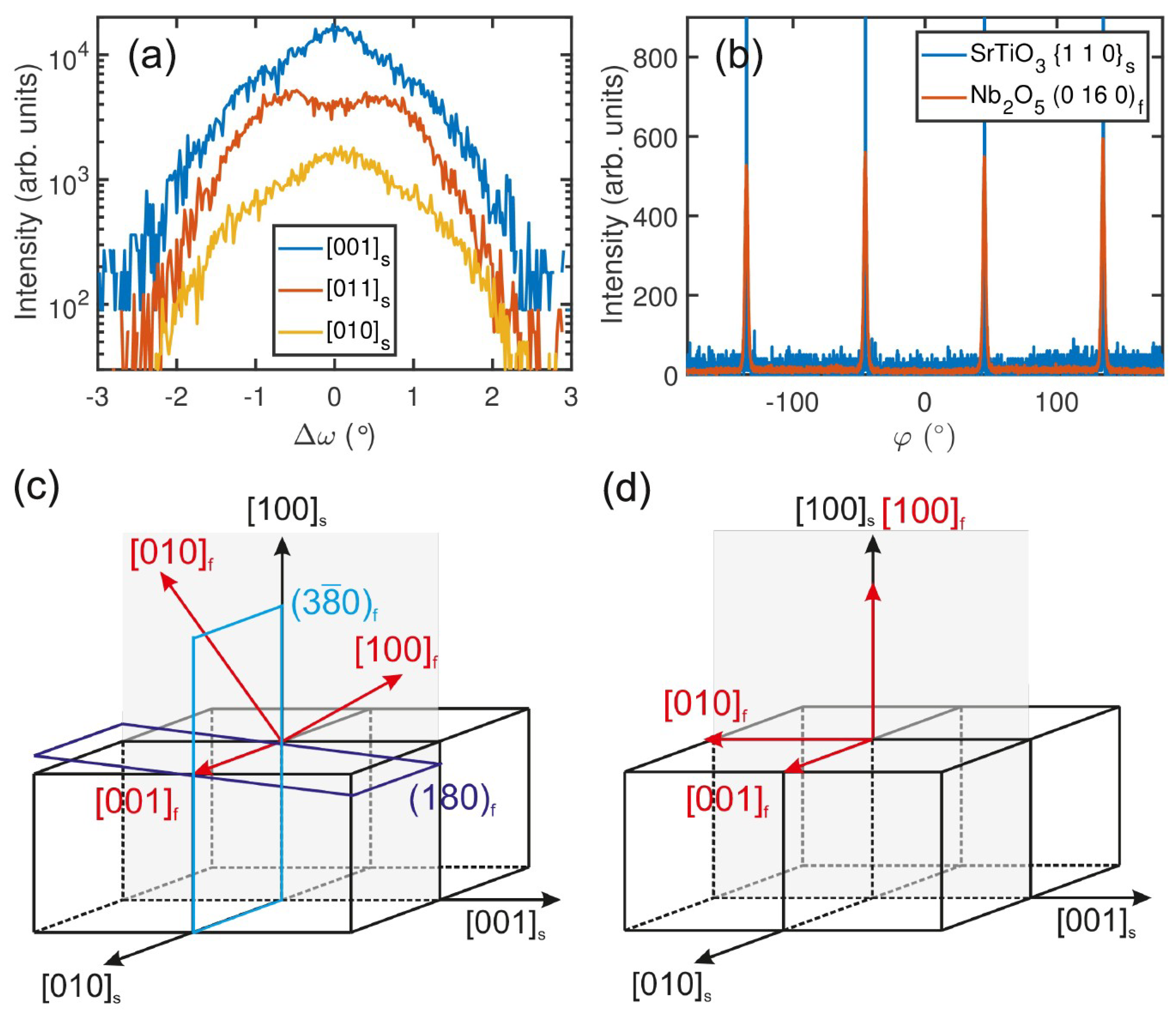
In the following, we investigate the effect of lattice parameter mismatch and the symmetry of the substrate on the film growth and domain formation. We first concentrate on the T-Nb2O5 films on (100)s-oriented SrTiO3 and analyze the epitaxial relationship in more detail. Figure 4a shows ω-scans of the (180)f diffraction peaks of a T-Nb2O5 film grown at 600 °C. The shape of the ω-scan depends on the in-plane orientation of the substrate relative to the incident X-ray beam. When the X-ray beam is parallel to the [011]s in-plane direction of the substrate, two peaks are observed at ±0.7°. In the case of X-rays parallel to the [010]s or [001]s in-plane directions of the (100)s SrTiO3 substrate, a maximum at ω = 0° and two shoulders at ω = ±1.0° are observed. The peak splitting points to the formation of domains which are tilted by ±ω = 1.0° with respect to the surface normal toward the [010]s and [001]s directions. In addition, φ-scans were performed in order to study the number of domains in more detail. The φ-scan, presented in Figure 4b, reveals the presence of four (0 16 0)f T-Nb2O5 peaks aligned with the SrTiO3 substrate, indicating that four T-Nb2O5 domain orientations are present in the film.
In order to understand these observations, the lattice mismatch between the T-Nb2O5 structure and (100)s SrTiO3 surface has to be considered. While the dimensions of the surface unit cell of (100)s SrTiO3 is given by 3.905 Å × 3.905 Å, the bulk lattice parameters of the orthorhombic T-Nb2O5 polymorph amount to a = 6.168 Å, b = 29.312 Å, and c = 3.938 Å [2]. According to the XRD data (Figure 2b), the films contain (200)f- and (180)f-oriented domains. For both orientations, the c-lattice parameter of T-Nb2O5 can be aligned with one in-plane direction of the (100)s SrTiO3 substrate, either along ±[010]s or ±[001]s. A schematic displaying both configurations of the crystallographic arrangement is given in Figure 4c,d. This epitaxial alignment results in a lattice mismatch of only −0.8% in the c-direction and is, therefore, expected to be energetically favorable. Since all in-plane variants are equivalent, there are four different in-plane orientations for the domains. This theoretical assumption of the presence of four different in-plane variants with (180)f orientation is in good agreement with the ω- and φ-scans that were performed on the (180)f and (0 16 0)f diffraction peaks, i.e., Figure 4a,b.
The in-plane lattice alignment of the (180)f-oriented domains in the direction orthogonal to the c-axis cannot be guessed intuitively, because there exists no low-indexed/highly symmetric lattice plane that is both orthogonal to the (001)f and (180)f planes. Instead, it is found that the (3−80)f plane makes an angle of 88.9° with the (180)f plane. Assuming that (3−80)f is parallel with the (001)s plane, the (180)f plane is tilted by α = −1.1° from the [001]s direction of the substrate, as shown schematically in Figure 4c. This tilt angle is in good agreement with the tilt angle determined from the ω-scans in Figure 2a (peak splitting by ∆ω ≈ 2°). Therefore, we conclude that the (3−80)f plane is indeed lying parallel to the (100)s plane of the SrTiO3 substrate. Finally, it is noted that the lattice mismatch in the direction orthogonal to the c-axis amounts to several percent and leads to a strong lattice relaxation in this direction.
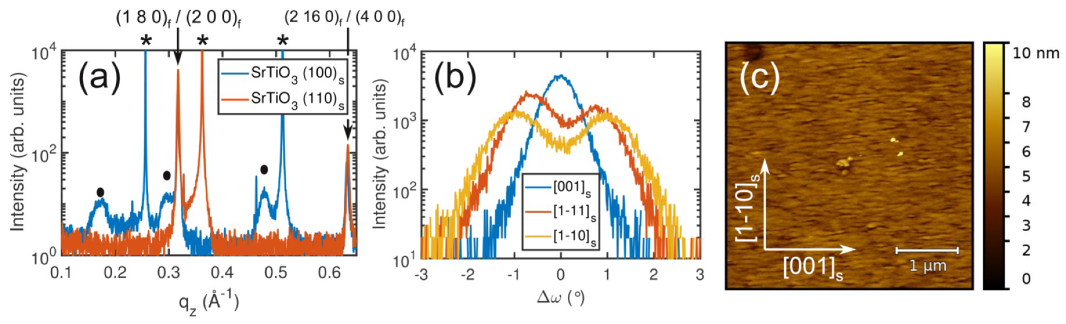
In contrast to the (100)s SrTiO3 surface, the (110)s SrTiO3 surface does not exhibit a fourfold rotational symmetry but only a twofold one. The surface unit cell amounts to d001 = 3.905 Å and d1–10 = 5.522 Å. Similar to the film growth on (100)s SrTiO3, only the unit cell dimension of (110)s SrTiO3 along the [001]s direction (d001 = 3.905 Å) fits to one of the lattice parameters of T-Nb2O5, namely the c-axis (c = 3.938 Å). Therefore, the number of domain orientations on SrTiO3 (110)s is expected to be reduced with respect to the SrTiO3 (100)s surface. Figure 5a shows that a pure T-Nb2O5 phase was grown on (110)s SrTiO3 at 600 °C. A comparison of the films grown on (100)s and (110)s SrTiO3 at 600 °C reveals that (i) on SrTiO3 (110)s, no H-Nb2O5 phase was additionally observed, and (ii) both films have a preferential (180)f out-of-plane direction, suggesting that this is the preferred growth direction. Furthermore, the (200)f out-of-plane orientation was not observed for films grown on SrTiO3(110)s within the experimental resolution. Again, the orientation of the domains in the film was studied by performing XRD ω-scans with the X-ray beam along different in-plane directions of the substrate, as indicated in Figure 5b. The data clearly differ from the case of growth on (100)s SrTiO3 substrates, because only a single peak is observed when the X-ray beam is parallel with the [001]s direction. This peak is—however—split for the scans in the [1−11]s and [1−10]s directions, indicating that there are two domain orientations present in films grown on (110)s SrTiO3 that have (180)f lattice planes that are tilted by approximately ±1° with respect to the [110]s orientation of the substrate. This tilt angle is the same as that in the case for T-Nb2O5 grown on (100)s SrTiO3. Therefore it is concluded that the (3−80)f plane is parallel with the (1−10)s plane of the SrTiO3 substrate. In addition, it was found that the reduction of the number of domain orientations results in a significant change of the surface morphology. Instead of the rough surface with fourfold rotational symmetry that is observed on (100)s-oriented substrates, the surface of the film grown on the (110)s-oriented SrTiO3 reflects the twofold symmetry, as observed by XRD, and has a root mean square surface roughness of 0.7 nm, as can be deduced from the data presented in Figure 5c.
The presented data thus show that the symmetry mismatch between T-Nb2O5 and SrTiO3 result in the formation of domains with different crystallographic orientations. Interestingly, the in-plane orientation is determined by the alignment of the T-Nb2O5 c-axis with the <001> directions of the substrate, whereas the out-of-plane direction is the same for thin films grown on (100)s- and (110)s-oriented SrTiO3. The latter could be due to a preferred growth direction and suggest that the structural coupling across the interface is weak, because, in the case of a strong coupling, the film orientation would be determined by the substrate orientation and would thus change when the substrate orientation changes.
3.3. TEM Investigations of the Microstructure
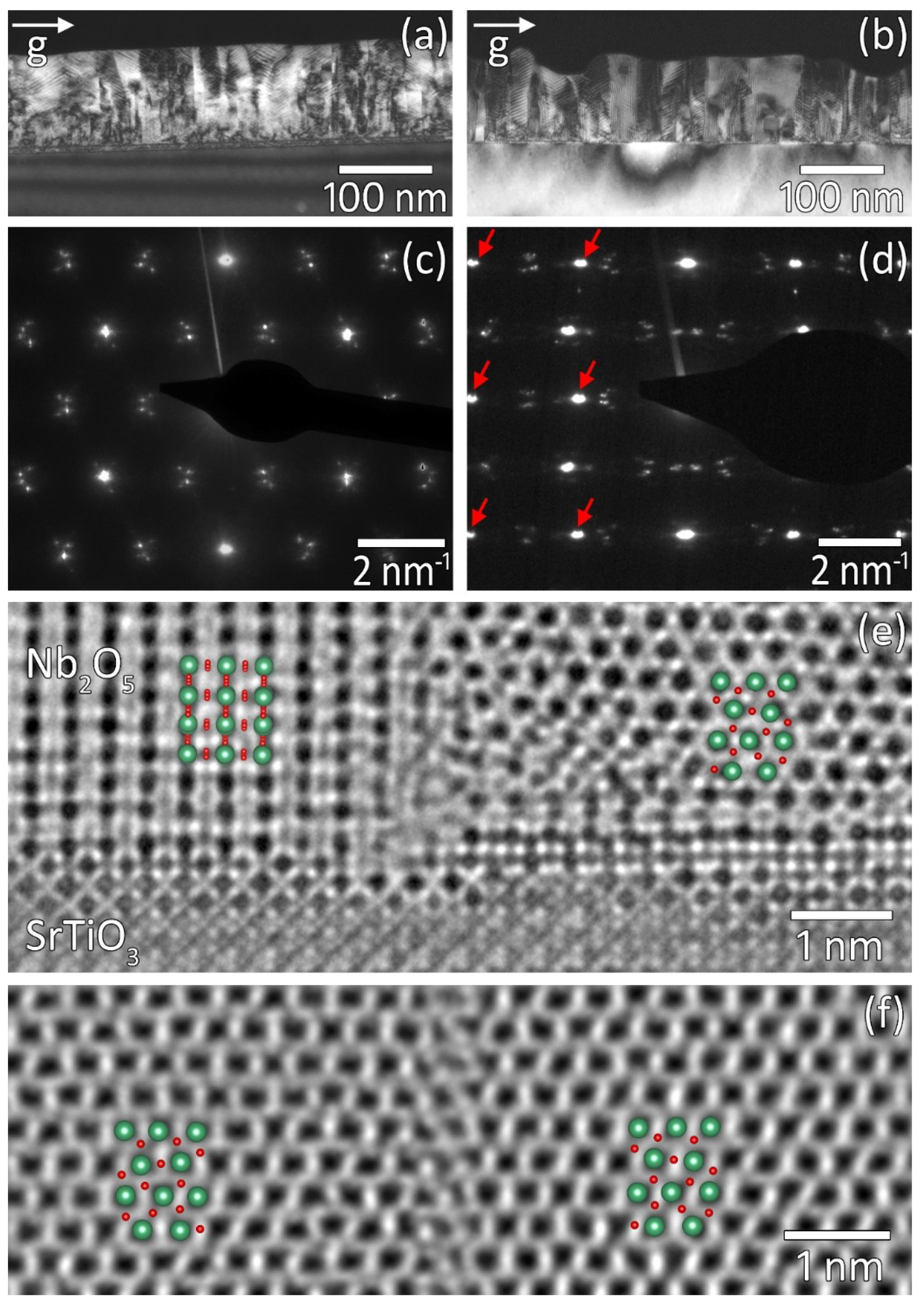
Up to now, we can summarize that the use of (110)s-oriented SrTiO3 substrates leads to a reduction in the number of in-plane rotational domain variants in T-Nb2O5 thin films from four to two. The domains have (180)f out-of-plane orientation with a tilt angle of about ±1° from the [110]s substrate surface normal. In the following, the structural properties of these films are analyzed in greater detail using transmission electron microscopy (TEM). Figure 6 shows cross-sectional TEM images of T-Nb2O5 films grown on (110)s- and (100)s-oriented SrTiO3 substrates, respectively. In agreement with our XRD measurements, electron diffraction (Figure 6c,d) and HRTEM imaging (Figure 6e,f) reveal that, in both cases, the film grows with (180)f orientation. Abrupt intensity variations within the T-Nb2O5 film for both substrate orientations in dark-field TEM images recorded close to the [001]s zone axis (see Figure 5a,b) point toward the presence of domains having a lateral size between 10 and 100 nm. The nature of these domains can be deduced by analyzing the electron diffraction and HRTEM data more carefully. In the case of the growth on a (100)s-oriented SrTiO3 substrate, two different HRTEM contrast patterns, i.e., domain types of the T-Nb2O5 film, were observed in images recorded in the [001]s zone axis. Since the HRTEM image shown in Figure 6e was recorded with a small underfocus of Δf ≈ −6 nm and a thickness of the TEM specimen of t ≈ 6 nm, the dark intensity minima in the film correspond to Nb-atomic columns. One type of domain appears in the HRTEM micrograph with a quasi-hexagonal pattern (see right part of Figure 6e). A simplified model of T-Nb2O5 adapted from Lee et al. [12] (Figure 1c) in the [001]f projection matches the HRTEM pattern very well. This type of domain thus grows with the epitaxial relationship [001]f parallel to [001]s. The second type of domain is characterized by a rectangular HRTEM pattern (see left part of Figure 6e), which matches very well to a model of T-Nb2O5 being rotated in-plane by 90° with respect to the first type of domain, i.e., the epitaxial relationship of these domains is [001]f perpendicular to [001]s. In the case of growth on (110)s-oriented substrates, only one type of domain was observed, namely, the one with the epitaxial relationship [001]f parallel to [001]s (see Figure 6f). Analyzing the Fourier transformation (not shown here) of that HRTEM image, we found that while the pure in-plane Fourier components of the neighboring domains (left and right side in Figure 6f) match with each other, their out-of-plane Fourier components are separated. This can be explained by a 180° in-plane rotation between the domains. The observed separation of the out-of-plane Fourier components corresponds to a tilt of the (180)f planes of the neighboring domains by approximately 2° with respect to each other. This, in fact, agrees very well with the results of the XRD measurements. The presence of variants of each domain type that are rotated in-plane by 180° leads finally to four and two possible differently oriented domains for T-Nb2O5 films grown on (100)s and (110)s SrTiO3 substrates, respectively.
These findings from the HRTEM analysis are also confirmed on a macroscopic scale by electron diffraction data recorded close to the [001]s zone axis. In the case of a (110)s SrTiO3 substrate, the diffraction image of the T-Nb2O5 film (see Figure 6c) shows only a quasi-hexagonal pattern. For the film grown on a (100)s-oriented substrate, there are additional reflections arranged in a rectangular way (mark by red arrows in Figure 6d) in the diffraction image. The weaker spots that appear in both diffraction images and that are split correspond to a periodic superstructure of approx. 3 nm in the films, which is consistent with previous observations [7].
4. Summary and Conclusions
We have shown that stable growth conditions can be realized for the epitaxial growth of T-Nb2O5 on different SrTiO3 surfaces by means of MOCVD. Moreover, the number of deposited in-plane domains could be reduced from four to two by the application of (110)s-oriented SrTiO3. This shows that heteroepitaxial growth can be used to improve the structural properties of T-Nb2O5 thin films. However, the lattice constant mismatch, as well as the more serious symmetry mismatch between the perovskite substrate and T-Nb2O5 film, make it challenging to achieve well-ordered epitaxial growth. So far, the growth of single crystalline films on (110)s SrTiO3 is hindered by the possible double orientation of nonequivalent 180° in-plane rotated Nb2O5 domains. Using substrates with an appropriate miscut might be a way to prevent the formation of the two in-plane domain variants and, therefore, to achieve heteroepitaxial growth of single crystalline T-Nb2O5 films.
Author Contributions
J.E.B. performed growth and XRD characterization of the films. T.M. analysed the films using TEM. The manuscript was written by J.E.B. and T.M. with assistance of J.S. and M.A. The work was supervised by J.S. and M.A.
Funding
This work was funded by the Leibniz association within the Leibniz Competition through a project entitled “Physics and control of defects in oxide films for adaptive electronics”.
Acknowledgments
We are grateful to M. Klann for technical support during MOCVD growth and to X.Y. for proofreading the manuscript. This work was performed in the framework of GraFOx, a Leibniz-Science Campus partially funded by the Leibniz association.
Conflicts of Interest
The authors declare no conflict of interest.
References
- Schäfer, H.; Gruehn, R.; Schulte, F. Die Modifikationen des Niobpentoxids. Angew. Chem. 1966, 78, 28–41. [Google Scholar] [CrossRef]
- Nico, C.; Monteiro, T.; Graça, M.P.F. Niobium oxides and niobates physical properties: Review and prospects. Prog. Mater. Sci. 2016, 80, 1–37. [Google Scholar] [CrossRef]
- Augustyn, V.; Come, J.; Lowe, M.A.; Kim, J.W.; Taberna, P.-L.; Tolbert, S.H.; Abruña, H.D.; Simon, P.; Dunn, B. High-rate electrochemical energy storage through Li+ intercalation pseudocapacitance. Nat. Mater. 2013, 12, 518–522. [Google Scholar] [CrossRef] [PubMed] [Green Version]
- Sun, H.; Mei, L.; Liang, J.; Zhao, Z.; Lee, C.; Fei, H.; Ding, M.; Lau, J.; Li, M.; Wang, C.; et al. Three-Dimensional Holey-Graphene/Niobia Composite Architectures for Ultrahigh-Rate Energy Storage. Science 2017, 356, 599–604. [Google Scholar] [CrossRef] [PubMed]
- Slesazeck, S.; Mähne, H.; Wylezich, H.; Wachowiak, A.; Radhakrishnan, J.; Ascoli, A.; Tetzlaff, R.; Mikolajick, T. Physical model of threshold switching in NbO2 based memristors. RSC Adv. 2015, 5, 102318–102322. [Google Scholar] [CrossRef]
- Slesazeck, S.; Rafaja, D.; Mikolajick, T. Filamentary resistive switching in amorphous and polycrystalline Nb2O5 thin films. Solid State Electron. 2012, 72, 73–77. [Google Scholar] [CrossRef]
- Spyridelis, J.; Delavignette, P.; Amelinckx, S. On the Superstructures of Ta2O5 and Nb2O5. Phys. Status Solidi 1967, 19, 683–704. [Google Scholar] [CrossRef]
- Stephenson, N.C.; Roth, R.S. The crystal structure of the high temperature form of Ta2O5. J. Solid State Chem. 1971, 3, 145–153. [Google Scholar] [CrossRef]
- Hellwig, M.; Milanov, A.; Barreca, D.; Deborde, J.L.; Thomas, R.; Winter, M.; Kunze, U.; Fischer, R.A.; Devi, A. Stabilization of amide-based complexes of niobium and tantalum using malonates as chelating ligands: Precursor chemistry and thin film deposition. Chem. Mater. 2007, 19, 6077–6087. [Google Scholar] [CrossRef]
- Fiz, R.; Appel, L.; Gutiérrez-Pardo, A.; Ramírez-Rico, J.; Mathur, S. Electrochemical Energy Storage Applications of CVD Grown Niobium Oxide Thin Films. ACS Appl. Mater. Interfaces 2016, 8, 21423–21430. [Google Scholar] [CrossRef] [PubMed] [Green Version]
- Kato, K.; Tamura, S. Die Kristallstruktur von T-Nb2O5. Acta Crystallogr. Sect. B Struct. Crystallogr. Cryst. Chem. 1975, 31, 673–677. [Google Scholar] [CrossRef]
- Lee, S.H.; Kim, J.; Kim, S.J.; Kim, S.; Park, G.S. Hidden structural order in orthorhombic Ta2O5. Phys. Rev. Lett. 2013, 110, 235502. [Google Scholar] [CrossRef] [PubMed]
- Momma, K.; Izumi, F. VESTA 3 for three-dimensional visualization of crystal, volumetric and morphology data. J. Appl. Crystallogr. 2011, 44, 1272–1276. [Google Scholar] [CrossRef]
- Manning, W.R.; Hunter, O.; Calderwood, F.W.; Stacy, D.W. Thermal expansion of Nb2O5. J. Am. Chem. Soc. 1971, 55, 342–347. [Google Scholar] [CrossRef]
- De Ligny, D.; Richet, P. High-temperature heat capacity and thermal expansion of SrTiO3 and SrZrO3 perovskites. Phys. Rev. B 1996, 53, 3013–3022. [Google Scholar] [CrossRef]
- Chason, E.; Guduru, P.R. Tutorial: Understanding residual stress in polycrystalline thin films through real-time measurements and physical models. J. Appl. Phys. 2016, 119, 191101. [Google Scholar] [CrossRef]
Figure 1.
Structural models of (a) H-Nb2O5 and (b,c) T-Nb2O5. The model in (b) is adapted from Kato et al. [11], and the model in (c) is adapted from Lee et al. [12].

Figure 2.
Wide range X-ray diffraction patterns of Nb2O5 thin films on SrTiO3 (100)s grown at different temperatures (a) and using different niobium ethoxide concentrations, i.e., different film growth rates, at a fixed growth temperature of 600 °C (d). (b) θ/2θ scans with higher magnification for the films grown at 450 °C, 500 °C, 550 °C, 600 °C, and 650 °C. (c) (180) Lattice parameter of T-Nb2O5 and the film thickness as a function of the deposition temperature. The dashed line in (c) shows the fitting of the data. The asterisks in (a,d) indicate the positions of the substrate peaks, whereas the circles refer to the peaks corresponding to the H-Nb2O5 phase.

Figure 3.
Surface morphology of T-Nb2O5 films grown on (100)s-oriented SrTiO3 using growth temperatures of (a) 450 °C, (b) 550 °C and (c) 650 °C, as determined by atomic force microscopy (AFM). The data reveal an increase in the grain size with increasing temperature. The arrows indicate the crystallographic directions of the substrate.

Figure 4.
(a) ω-scans of the (180)f diffraction peak with the X-ray beam parallel to different in-plane directions of the substrate, as indicated in the inset. (b) φ-scans of the SrTiO3 {110}s diffraction peaks and the T-Nb2O5 (0 16 0)f diffraction peak. The observation of four T-Nb2O5 (0 16 0)f peaks indicates that four grain orientations are present in the film. (c,d) Schematics of the crystallographic relationship between the SrTiO3 substrate and (180)f-oriented T-Nb2O5 and (100)f-oriented T-Nb2O5, respectively. The indices “f” and “s” denote directions corresponding to the film and the substrate, respectively.

Figure 5.
(a) Comparison of the XRD profiles of T-Nb2O5 on (100)s SrTiO3 (blue) and (110)s SrTiO3 (red). The peaks associated with the substrate and H-Nb2O5 are marked with an asterisk and filled circles, respectively. (b) ω-scans of the (180)f diffraction peak with the X-ray beam parallel to different in-plane directions for T-Nb2O5 on SrTiO3 (110)s. (c) Surface morphology of T-Nb2O5 on SrTiO3 (110)s film as determined by AFM (c). The root mean square surface roughness is 0.7 nm. The crystallographic directions of the substrate are indicated by the arrows.

Figure 6.
Cross-sectional TEM images of Nb2O5 films grown on SrTiO3. (a,c,f) (110)s-oriented substrate, (b,d,e) (100)s-oriented substrate. (a,b) TEM dark field, (c,d) electron diffraction, and (e,f) HRTEM image, where the insets show models of T-Nb2O5 (green and red balls denote Nb and O, respectively).

© 2018 by the authors. Licensee MDPI, Basel, Switzerland. This article is an open access article distributed under the terms and conditions of the Creative Commons Attribution (CC BY) license (http://creativecommons.org/licenses/by/4.0/).
Share and Cite
MDPI and ACS Style
Boschker, J.E.; Markurt, T.; Albrecht, M.; Schwarzkopf, J. Heteroepitaxial Growth of T-Nb2O5 on SrTiO3. Nanomaterials 2018, 8, 895. https://doi.org/10.3390/nano8110895
AMA Style
Boschker JE, Markurt T, Albrecht M, Schwarzkopf J. Heteroepitaxial Growth of T-Nb2O5 on SrTiO3. Nanomaterials. 2018; 8(11):895. https://doi.org/10.3390/nano8110895
Chicago/Turabian StyleBoschker, Jos E., Toni Markurt, Martin Albrecht, and Jutta Schwarzkopf. 2018. "Heteroepitaxial Growth of T-Nb2O5 on SrTiO3" Nanomaterials 8, no. 11: 895. https://doi.org/10.3390/nano8110895
Note that from the first issue of 2016, this journal uses article numbers instead of page numbers. See further details here.