
Fabrication of Silicon Nanobelts and Nanopillars by Soft Lithography for Hydrophobic and Hydrophilic Photonic Surfaces


Abstract
:1. Introduction
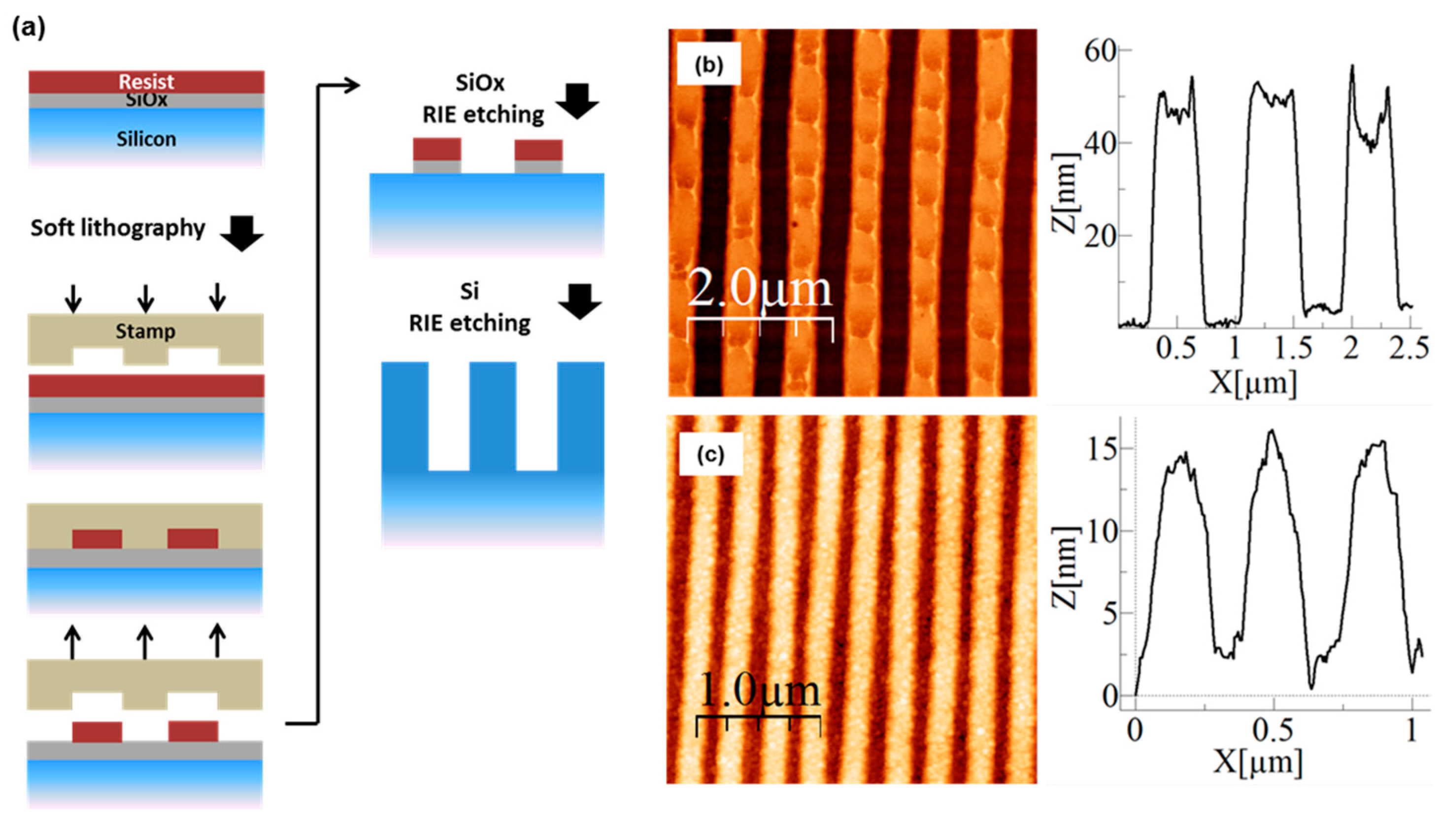
2. Experiment
3. Results and Discussion
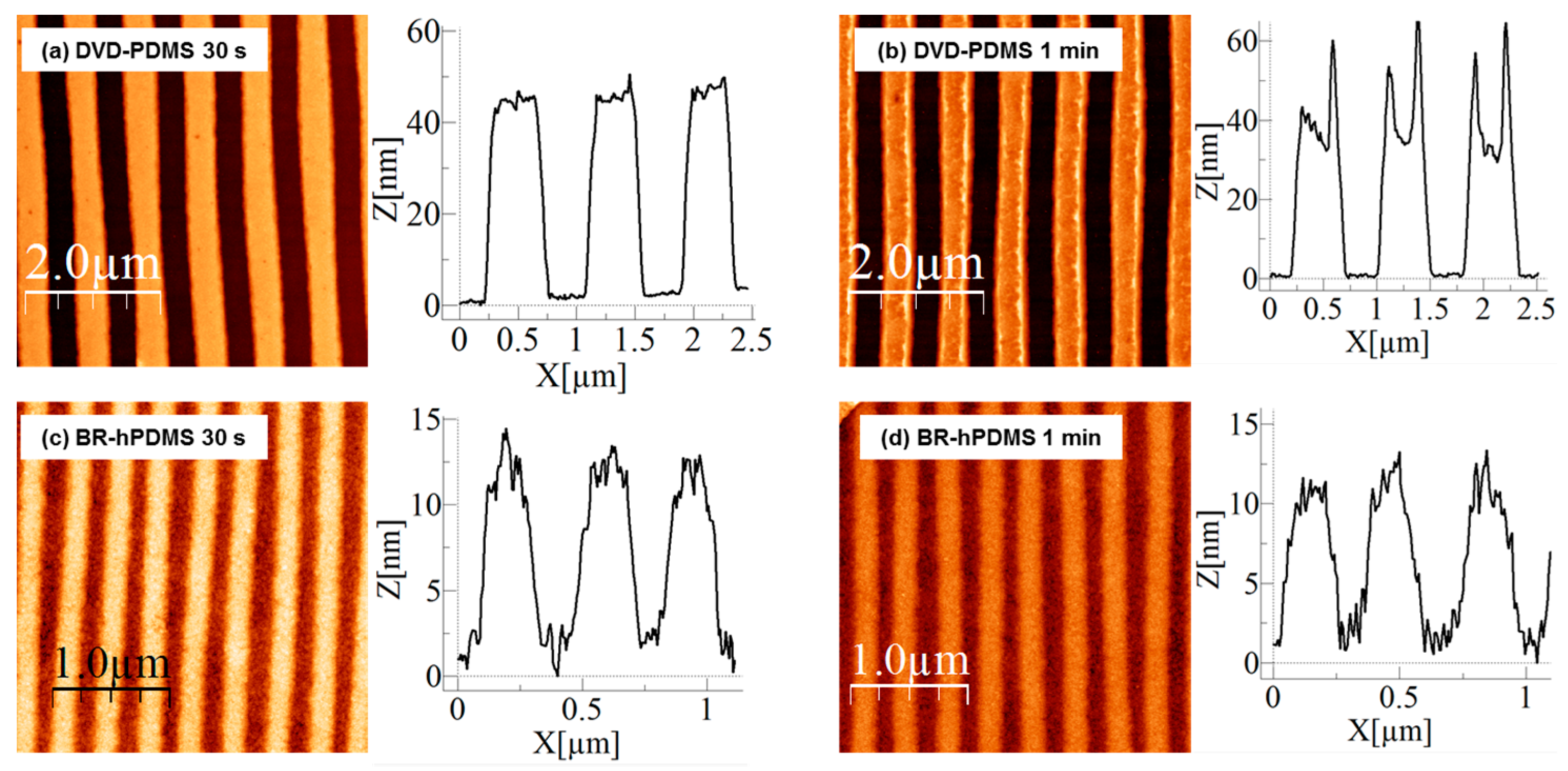
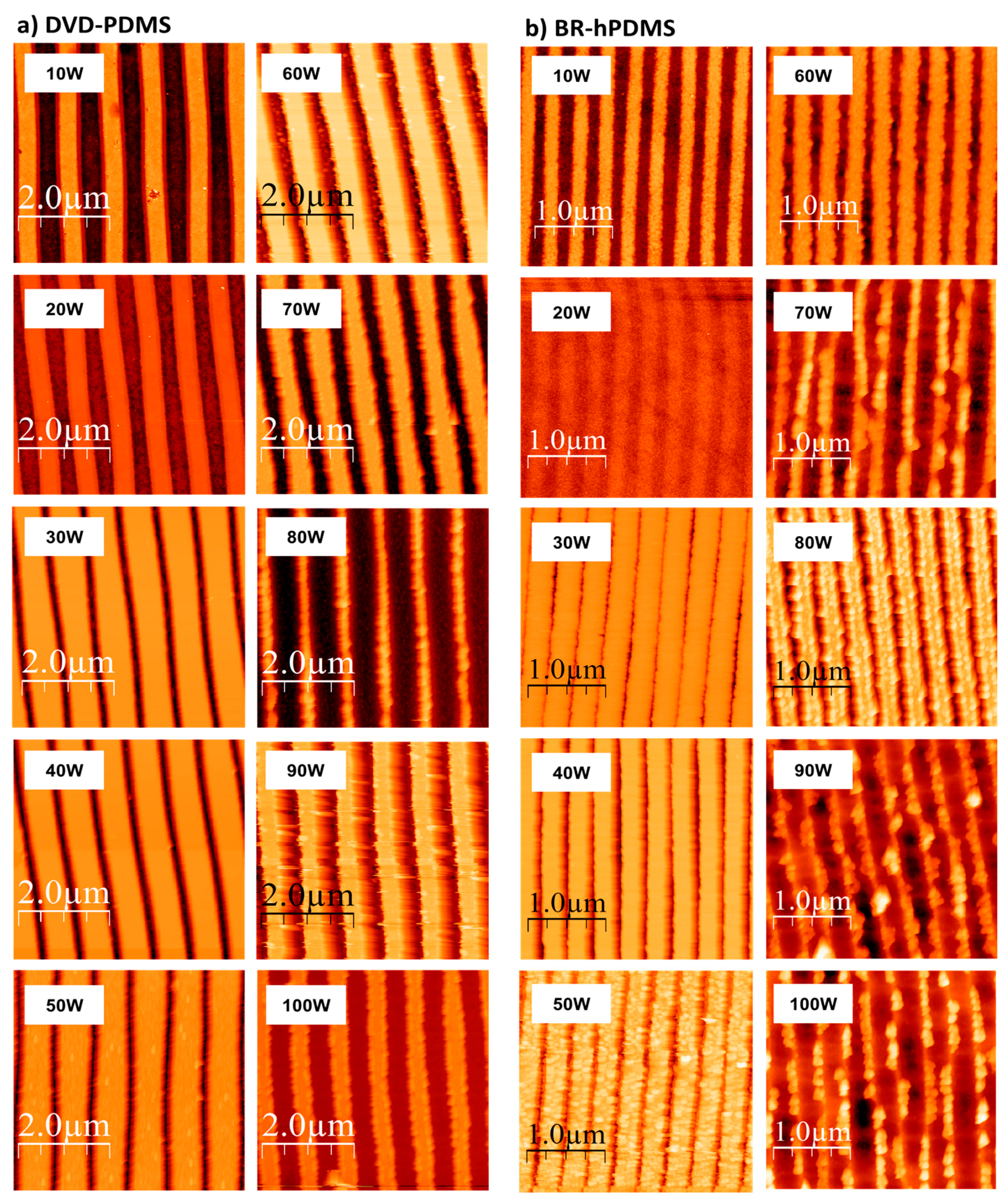
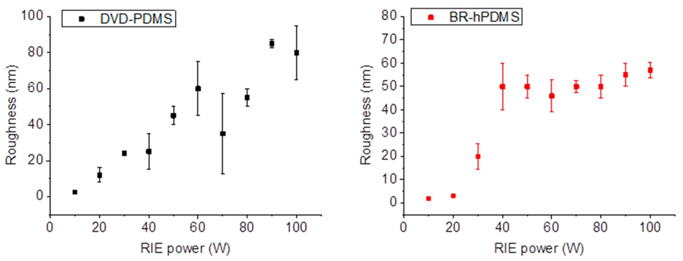
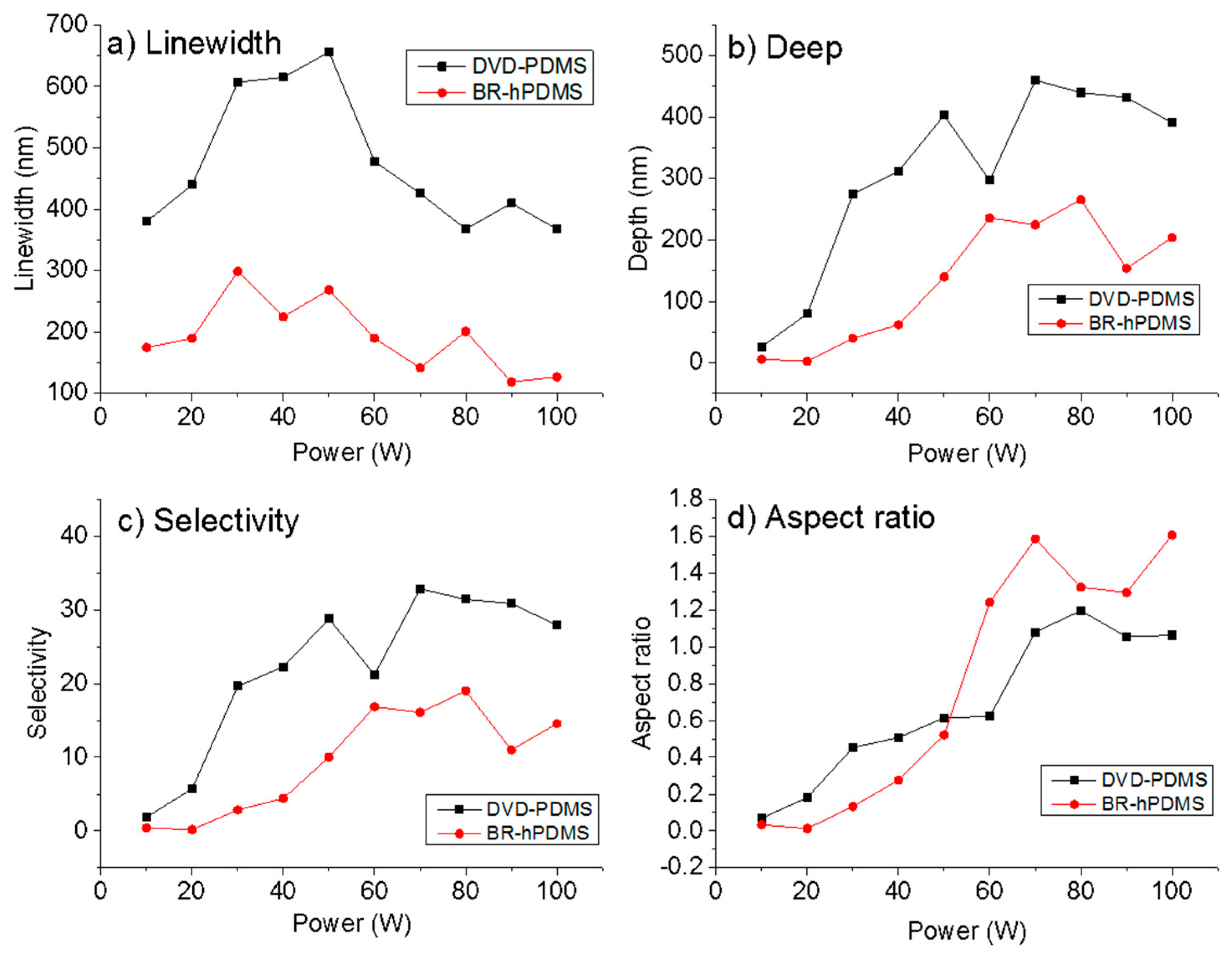
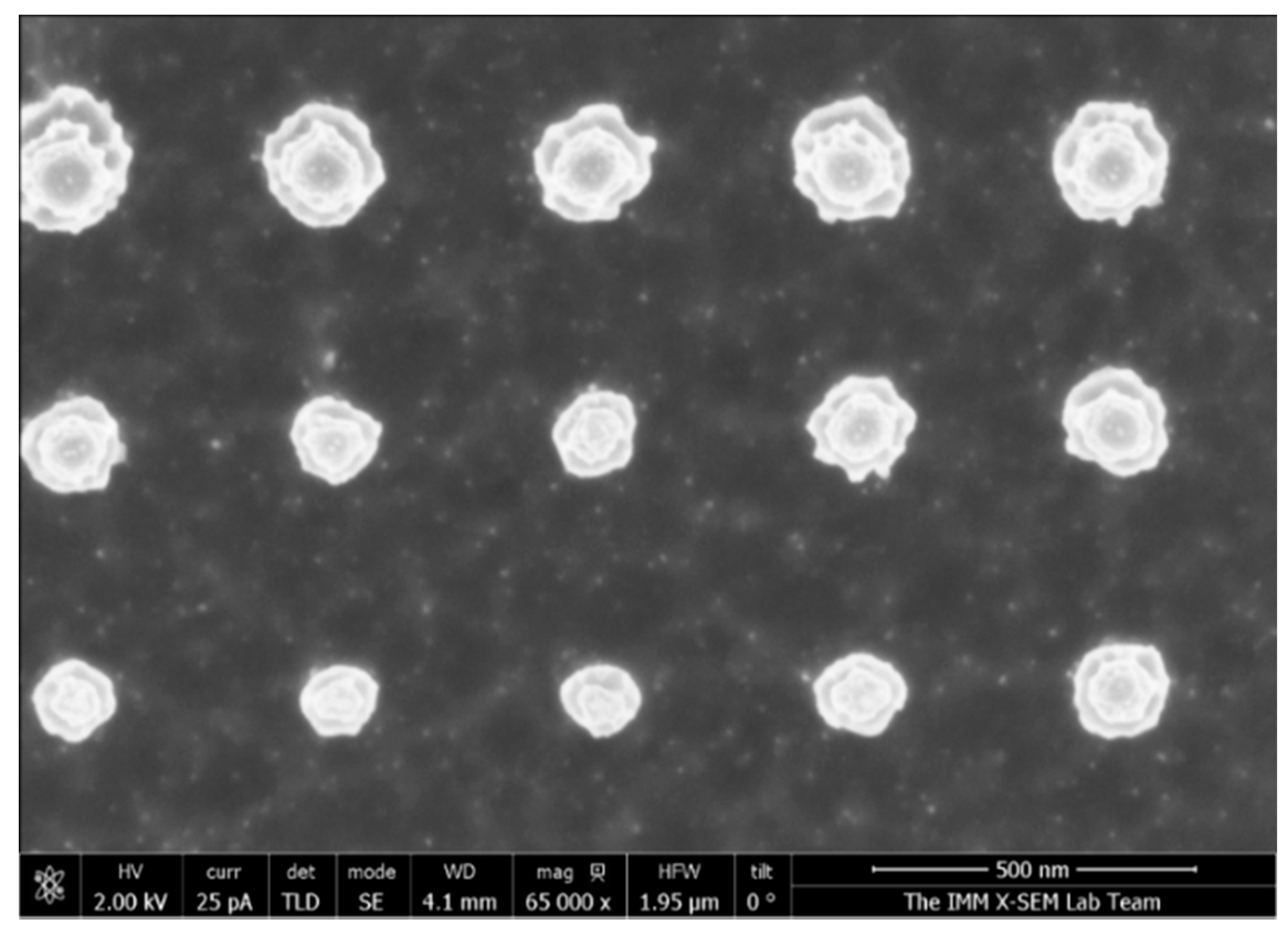
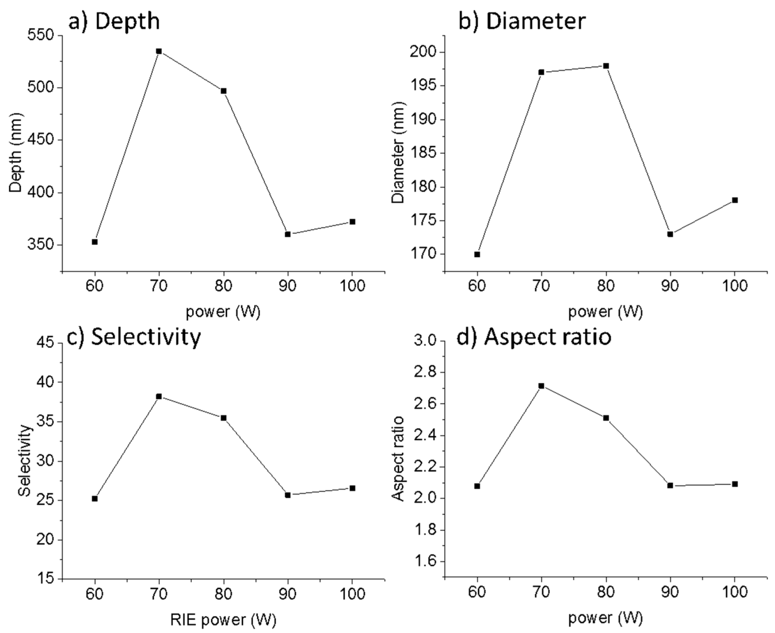
3.1. Optimization of the RIE Process
3.2. Wettability
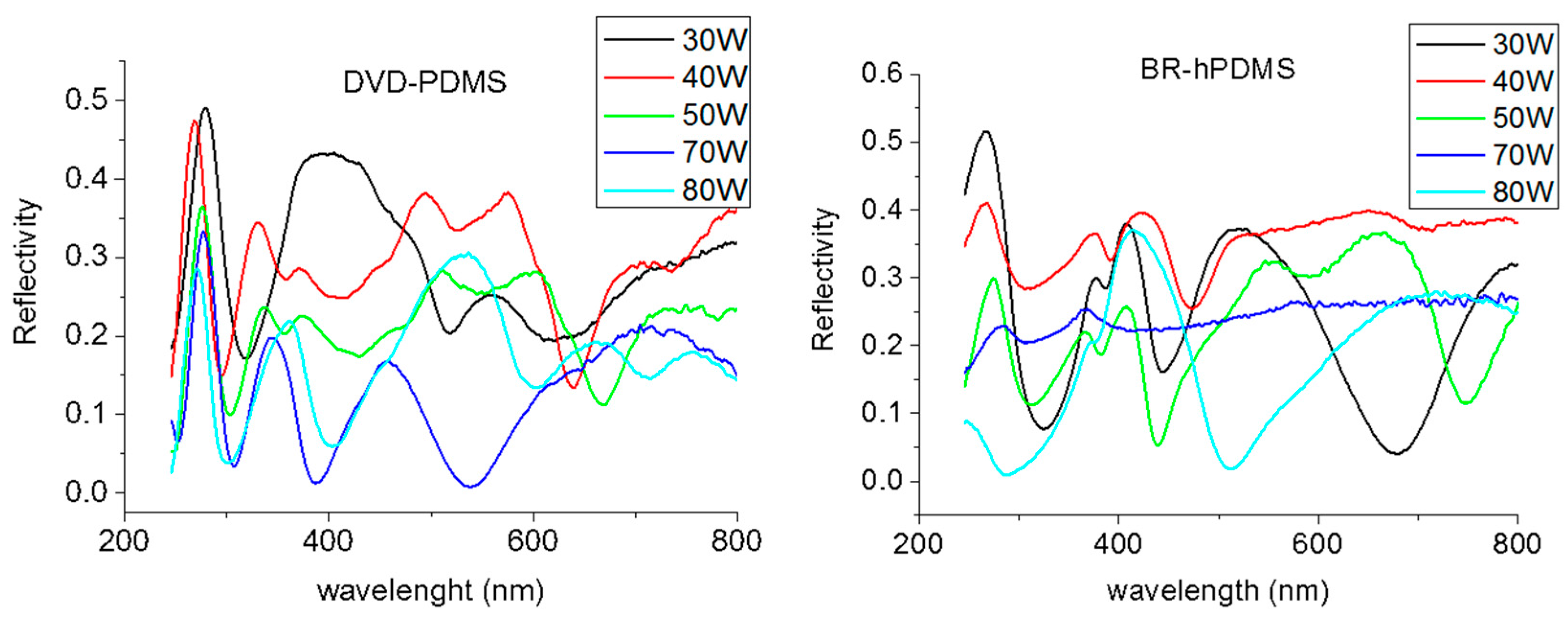
3.3. Optical Measurements
4. Conclusions
Supplementary Materials
Acknowledgments
Author Contributions
Conflicts of Interest
References
- Lenert, A.; Bierman, D.M.; Nam, Y.; Chan, W.R.; Celanovic, I.; Soljacic, M.; Wang, E.N. A nanophotonic solar thermophotovoltaic device. Nat. Nanotechnol. 2014, 9, 126–130. [Google Scholar] [CrossRef] [PubMed]
- Ferrini, R.; Houdré, R.; Benisty, H.; Qiu, M.; Moosburger, J. Radiation losses in planar photonic crystals: two-dimensional representation of hole depth and shape by an imaginary dielectric constant. JOSA B 2003, 20, 469–478. [Google Scholar] [CrossRef]
- Grimes, A.; Breslauer, D.N.; Long, M.; Pegan, J.; Lee, L.P.; Khine, M. Shrinky-Dink microfluidics: Rapid generation of deep and rounded patterns. Lab Chip 2008, 8, 170–172. [Google Scholar] [CrossRef] [PubMed]
- Anderson, J.R.; Chiu, D.T.; Wu, H.; Schueller, O.; Whitesides, G.M. Fabrication of microfluidic systems in poly(dimethylsiloxane). Electrophoresis 2000, 21, 27–40. [Google Scholar]
- Lorenz, H.; Despont, M.; Fahrni, N.; Brugger, J.; Vettiger, P.; Renaud, P. High-aspect-ratio, ultrathick, negative-tone near-UV photoresist and its applications for MEMS. Sens. Actuators A Phys. 1998, 64, 33–39. [Google Scholar] [CrossRef]
- Simpson, P.C.; Roach, D.; Woolley, A.T.; Thorsen, T.; Johnston, R.; Sensabaugh, G.F.; Mathies, R.A. High-throughput genetic analysis using microfabricated 96-sample capillary array electrophoresis microplates. Proc. Natl. Acad. Sci. USA 1998, 95, 2256–2261. [Google Scholar] [CrossRef] [PubMed]
- Santos, A.; Deen, M.; Marsal, L. Low-cost fabrication technologies for nanostructures: State-of-the-art and potential. Nanotechnology 2015, 26, 042001. [Google Scholar] [CrossRef] [PubMed]
- Xia, Y.; Whitesides, G.M. Soft lithography. Annu. Rev. Mater. Sci. 1998, 28, 153–184. [Google Scholar] [CrossRef]
- Huang, Y.Y.; Zhou, W.; Hsia, K.; Menard, E.; Park, J.-U.; Rogers, J.A.; Alleyne, A.G. Stamp collapse in soft lithography. Langmuir 2005, 21, 8058–8068. [Google Scholar] [CrossRef] [PubMed]
- Wang, Z.-H.; Liu, W.; Zuo, Q.; Wang, L.; Zhao, Y.-L.; Xu, Z.-M. Enhanced Depth of Lift-off Pattern Defined with Soft Mold Ultraviolet Nanoimprint by Multi-Layer Masks. Chin. Phys. Lett. 2014, 31, 088102. [Google Scholar] [CrossRef]
- Kooy, N.; Mohamed, K.; Pin, L.T.; Guan, O.S. A review of roll-to-roll nanoimprint lithography. Nanoscale Res. Lett. 2014, 9, 320. [Google Scholar] [CrossRef] [PubMed]
- Alayo, N.; Conde-Rubio, A.; Bausells, J.; Borrisé, X.; Labarta, A.; Batlle, X.; Pérez-Murano, F. Nanoparticles with tunable shape and composition fabricated by nanoimprint lithography. Nanotechnology 2015, 26, 445302. [Google Scholar] [CrossRef] [PubMed]
- Lee, D.-H.; Park, K.-H.; Hong, L.-Y.; Kim, D.-P. SiCN ceramic patterns fabricated by soft lithography techniques. Sens. Actuators A Phys. 2007, 135, 895–901. [Google Scholar] [CrossRef]
- Miyamura, Y.; Park, C.; Kinbara, K.; Leibfarth, F.A.; Hawker, C.J.; Aida, T. Controlling volume shrinkage in soft lithography through heat-induced cross-linking of patterned nanofibers. J. Am. Chem. Soc. 2011, 133, 2840–2843. [Google Scholar] [CrossRef] [PubMed]
- Chen, B.; Mathai, C.J.; Mukherjee, S.; Gangopadhyay, S. Indium Tin Oxide Photonic Crystal for Controllable Light Coupling in Solar Cells by an Inexpensive Soft Lithography with HD-DVD and Blu-ray. ECS Trans. 2014, 61, 69–82. [Google Scholar] [CrossRef]
- Wu, B.; Kumar, A.; Pamarthy, S. High aspect ratio silicon etch: A review. J. Appl. Phys. 2010, 108, 051101. [Google Scholar] [CrossRef]
- Inomata, Y.; Fukui, K.; Shirasawa, K. Surface texturing of large area multicrystalline silicon solar cells using reactive ion etching method. Sol. Energy Mater. Sol. Cells 1997, 48, 237–242. [Google Scholar] [CrossRef]
- Tezani, L.; Pessoa, R.; Maciel, H.; Petraconi, G. Chemistry studies of SF6/CF4, SF6/O2 and CF4/O2 gas phase during hollow cathode reactive ion etching plasma. Vacuum 2014, 106, 64–68. [Google Scholar] [CrossRef]
- Picard, A.; Turban, G.; Grolleau, B. Plasma diagnostics of a SF6 radiofrequency discharge used for the etching of silicon. J. Phys. D Appl. Phys. 1986, 19, 991. [Google Scholar] [CrossRef]
- Marty, F.; Rousseau, L.; Saadany, B.; Mercier, B.; Français, O.; Mita, Y.; Bourouina, T. Advanced etching of silicon based on deep reactive ion etching for silicon high aspect ratio microstructures and three-dimensional micro-and nanostructures. Microelectron. J. 2005, 36, 673–677. [Google Scholar] [CrossRef]
- Mirza, M.M.; Zhou, H.; Velha, P.; Li, X.; Docherty, K.E.; Samarelli, A.; Ternent, G.; Paul, D.J. Nanofabrication of high aspect ratio (~50:1) sub-10 nm silicon nanowires using inductively coupled plasma etching. J. Vac. Sci. Technol. B 2012, 30, 06FF2. [Google Scholar] [CrossRef]
- Chang, Y.-F.; Chou, Q.-R.; Lin, J.-Y.; Lee, C.-H. Fabrication of high-aspect-ratio silicon nanopillar arrays with the conventional reactive ion etching technique. Appl. Phys. A 2007, 86, 193–196. [Google Scholar] [CrossRef]
- Qin, D.; Xia, Y.; Whitesides, G.M. Soft lithography for micro-and nanoscale patterning. Nat. Protoc. 2010, 5, 491–502. [Google Scholar] [CrossRef] [PubMed]
- Ryu, Y.K.; Postigo, P.A.; Garcia, F.; Garcia, R. Fabrication of sub-12 nm thick silicon nanowires by processing scanning probe lithography masks. Appl. Phys. Lett. 2014, 104, 223112. [Google Scholar]
- Hou, X.; Hu, Y.; Grinthal, A.; Khan, M.; Aizenberg, J. Liquid-based gating mechanism with tunable multiphase selectivity and antifouling behaviour. Nature 2015, 519, 70–73. [Google Scholar] [CrossRef] [PubMed]
- Zhang, Y.; Chen, Y.; Shi, L.; Li, J.; Guo, Z. Recent progress of double-structural and functional materials with special wettability. J. Mater. Chem. 2012, 22, 799–815. [Google Scholar] [CrossRef]
- Sun, T.; Feng, L.; Gao, X.; Jiang, L. Bioinspired surfaces with special wettability. Acc. Chem. Res. 2005, 38, 644–652. [Google Scholar] [CrossRef] [PubMed]
- Park, K.-C.; Choi, H.J.; Chang, C.-H.; Cohen, R.E.; McKinley, G.H.; Barbastathis, G. Nanotextured silica surfaces with robust superhydrophobicity and omnidirectional broadband supertransmissivity. ACS Nano 2012, 6, 3789–3799. [Google Scholar] [CrossRef] [PubMed]
- Wenzel, R.N. Resistance of solid surfaces to wetting by water. Ind. Eng. Chem. 1936, 28, 988–994. [Google Scholar] [CrossRef]
- Cassie, A.; Baxter, S. Wettability of porous surfaces. Trans. Faraday Soc. 1944, 40, 546–551. [Google Scholar] [CrossRef]
- Bhushan, B.; Jung, Y.C.; Koch, K. Micro-, nano-and hierarchical structures for superhydrophobicity, self-cleaning and low adhesion. Philos. Trans. R. Soc. Lond. A 2009, 367, 1631–1672. [Google Scholar] [CrossRef] [PubMed]
- Lau, K.K.; Bico, J.; Teo, K.B.; Chhowalla, M.; Amaratunga, G.A.; Milne, W.I.; McKinley, G.H.; Gleason, K.K. Superhydrophobic carbon nanotube forests. Nano Lett. 2003, 3, 1701–1705. [Google Scholar] [CrossRef]
- Tuteja, A.; Choi, W.; Mabry, J.M.; McKinley, G.H.; Cohen, R.E. Robust omniphobic surfaces. Proc. Natl. Acad. Sci.USA 2008, 105, 18200–18205. [Google Scholar] [CrossRef] [PubMed]
- Journet, C.; Moulinet, S.; Ybert, C.; Purcell, S.T.; Bocquet, L. Contact angle measurements on superhydrophobic carbon nanotube forests: Effect of fluid pressure. EPL 2005, 71, 104–109. [Google Scholar] [CrossRef]
- Flory, F.; Escoubas, L.; Berginc, G. Optical properties of nanostructured materials: A review. J. Nanophotonics 2011, 5, 52502–52520. [Google Scholar] [CrossRef]
- Lakowicz, J.R. Principles of Fluorescence Spectroscopy; Springer Science & Business Media: Berlin, Germany, 2013. [Google Scholar]


| RIE Power | ||||||||||
|---|---|---|---|---|---|---|---|---|---|---|
| 10 W | 20 W | 30 W | 40 W | 50 W | 60 W | 70 W | 80 W | 90 W | 100 W | |
| Roughness (nm) | 2.1 | 8 | 24.5 | 35 | 40 | 45 | 57.5 | 50 | 87.5 | 65 |
| Linewidth (nm) | 380 | 440 | 607 | 615 | 656 | 478 | 426 | 368 | 410 | 368 |
| Depth (nm) | 26.5 | 80 | 275 | 312 | 403 | 297 | 460 | 440 | 432 | 391 |
| Selectivity SiOx/Si | 1.8 | 5.7 | 19.6 | 22.2 | 28.7 | 21.2 | 32.8 | 31.4 | 30.85 | 27.92 |
| Aspect Ratio | 0.07 | 0.18 | 0.45 | 0.51 | 0.61 | 0.62 | 1.08 | 1.19 | 1.05 | 1.06 |
| RIE Power | ||||||||||
|---|---|---|---|---|---|---|---|---|---|---|
| 10 W | 20 W | 30 W | 40 W | 50 W | 60 W | 70 W | 80 W | 90 W | 100 W | |
| Roughness (nm) | 2.5 | 2.5 | 25.5 | 60 | 45 | 53 | 47.5 | 55 | 50 | 53.5 |
| Linewidth (nm) | 175 | 190 | 299 | 225 | 269 | 190 | 142 | 201 | 119 | 127 |
| Depth (nm) | 5.96 | 2.52 | 40 | 62 | 140 | 236 | 225 | 266 | 154 | 204 |
| Selectivity SiOx/Si | 0.42 | 0.18 | 2.85 | 4.42 | 10 | 16.85 | 16.07 | 19 | 11 | 16.57 |
| Aspect Ratio | 0.03 | 0.01 | 0.13 | 0.27 | 0.52 | 1.24 | 1.58 | 1.32 | 1.29 | 1.61 |
| RIE Power | |||||
|---|---|---|---|---|---|
| 60 W | 70 W | 80 W | 90 W | 100 W | |
| Diameter (nm) | 170 | 197 | 198 | 173 | 178 |
| Depth (nm) | 353 | 535 | 497 | 360 | 372 |
| Selectivity SiOx/Si | 25.2 | 38.2 | 35.5 | 25.7 | 26.5 |
| Aspect Ratio | 2.07 | 2.71 | 2.51 | 2.08 | 2.09 |
© 2017 by the authors. Licensee MDPI, Basel, Switzerland. This article is an open access article distributed under the terms and conditions of the Creative Commons Attribution (CC BY) license (http://creativecommons.org/licenses/by/4.0/).
Share and Cite
Baquedano, E.; Martinez, R.V.; Llorens, J.M.; Postigo, P.A. Fabrication of Silicon Nanobelts and Nanopillars by Soft Lithography for Hydrophobic and Hydrophilic Photonic Surfaces. Nanomaterials 2017, 7, 109. https://doi.org/10.3390/nano7050109
Baquedano E, Martinez RV, Llorens JM, Postigo PA. Fabrication of Silicon Nanobelts and Nanopillars by Soft Lithography for Hydrophobic and Hydrophilic Photonic Surfaces. Nanomaterials. 2017; 7(5):109. https://doi.org/10.3390/nano7050109
Chicago/Turabian StyleBaquedano, Estela, Ramses V. Martinez, José M. Llorens, and Pablo A. Postigo. 2017. "Fabrication of Silicon Nanobelts and Nanopillars by Soft Lithography for Hydrophobic and Hydrophilic Photonic Surfaces" Nanomaterials 7, no. 5: 109. https://doi.org/10.3390/nano7050109