
Solution-Mediated Inversion of SnSe to Sb2Se3 Thin-Films

 , , and
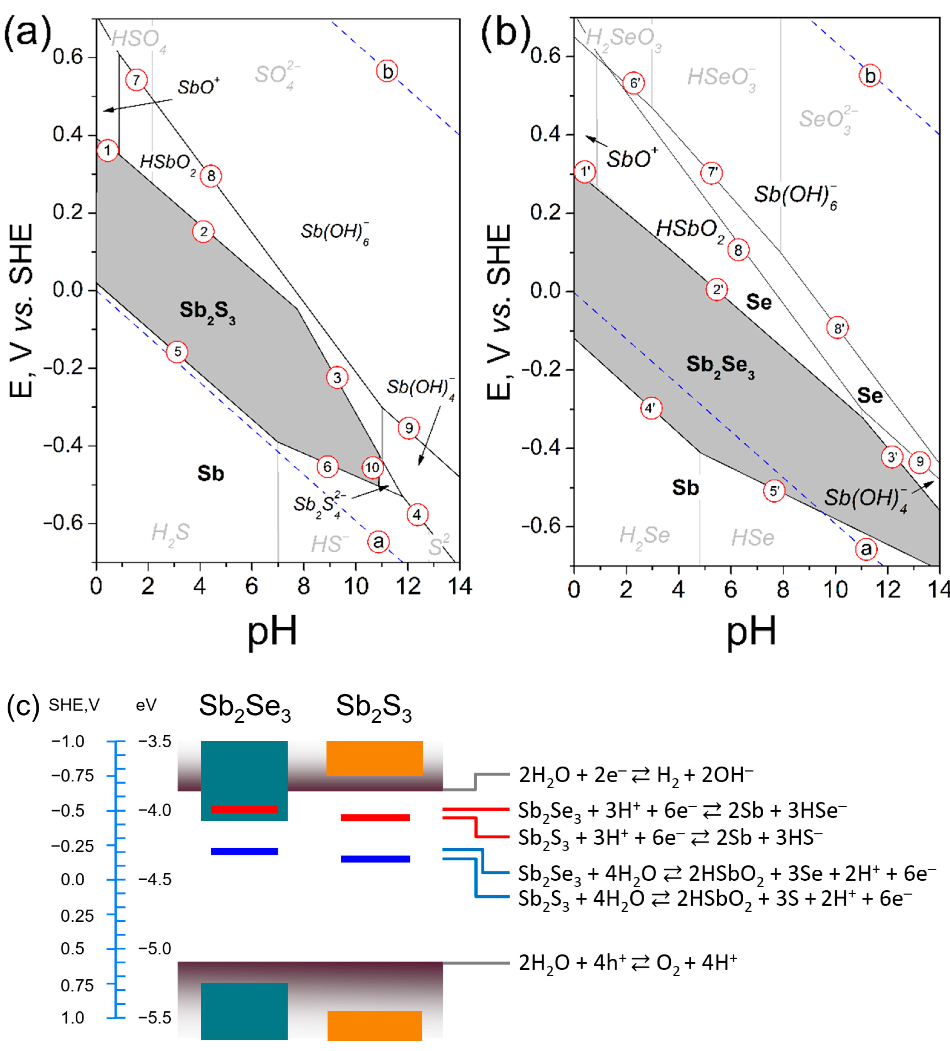
Abstract
:1. Introduction
2. Results and Discussion
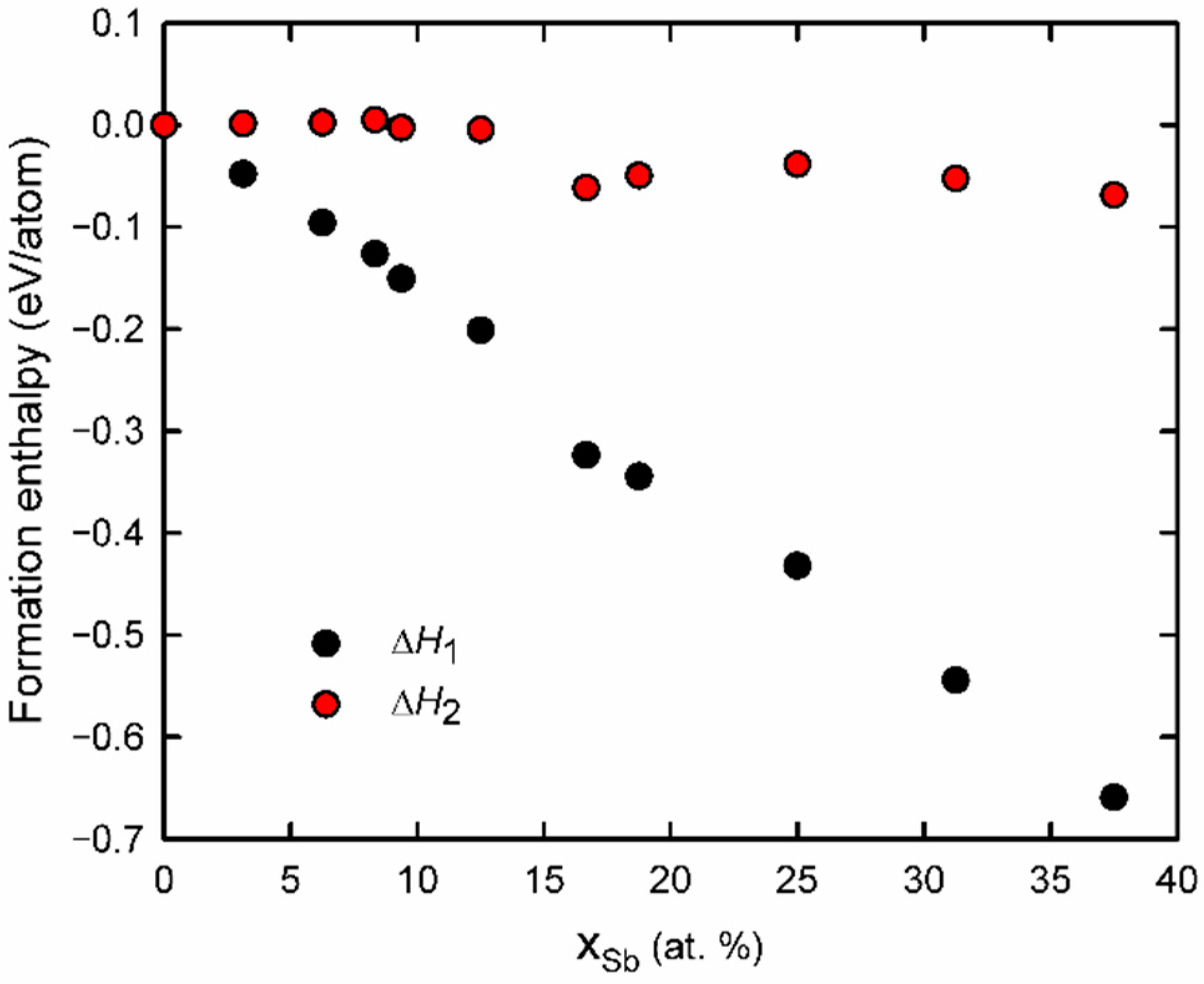
2.1. Discussion on the Stability of Antimony Selenide (Sulfide)
2.2. Ion Exchange from SnSe to Sb2Se3
2.2.1. Preliminary Trials
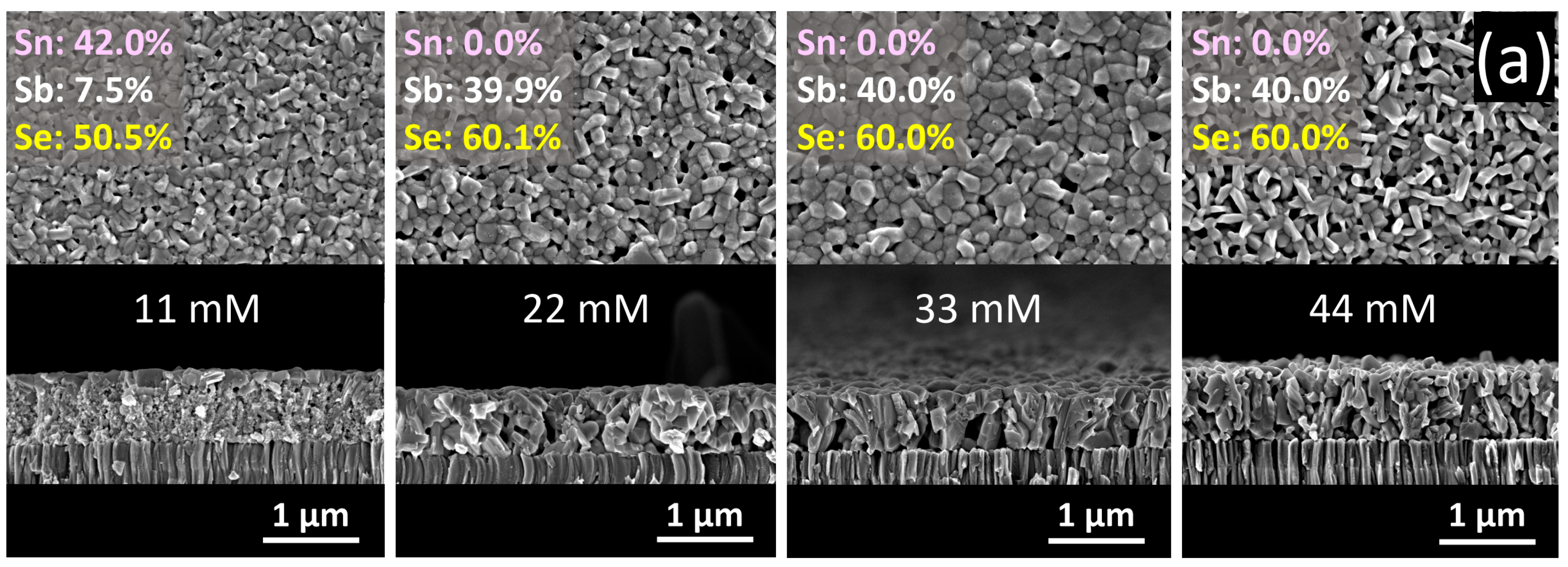
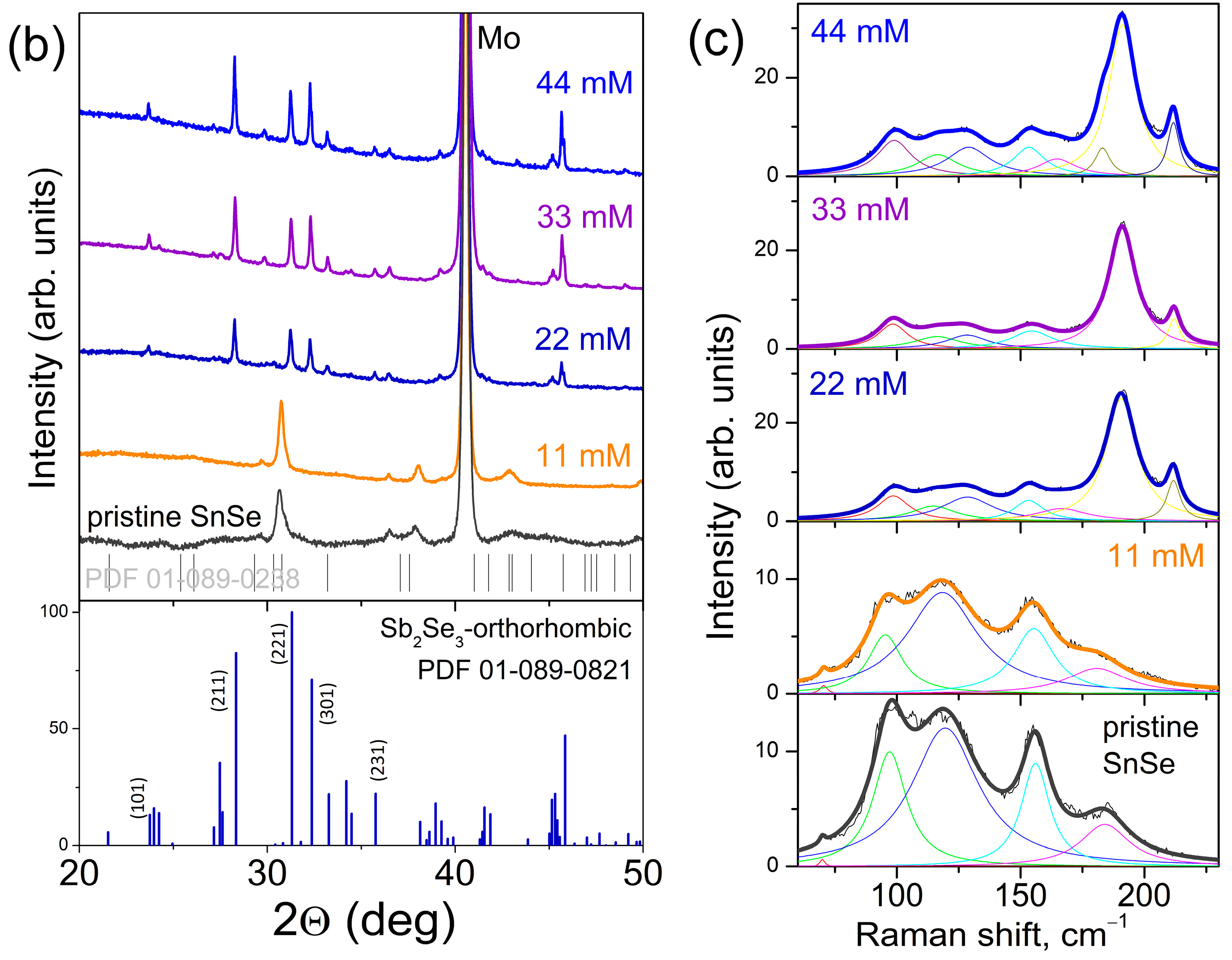
2.2.2. Concentration of SbCl3
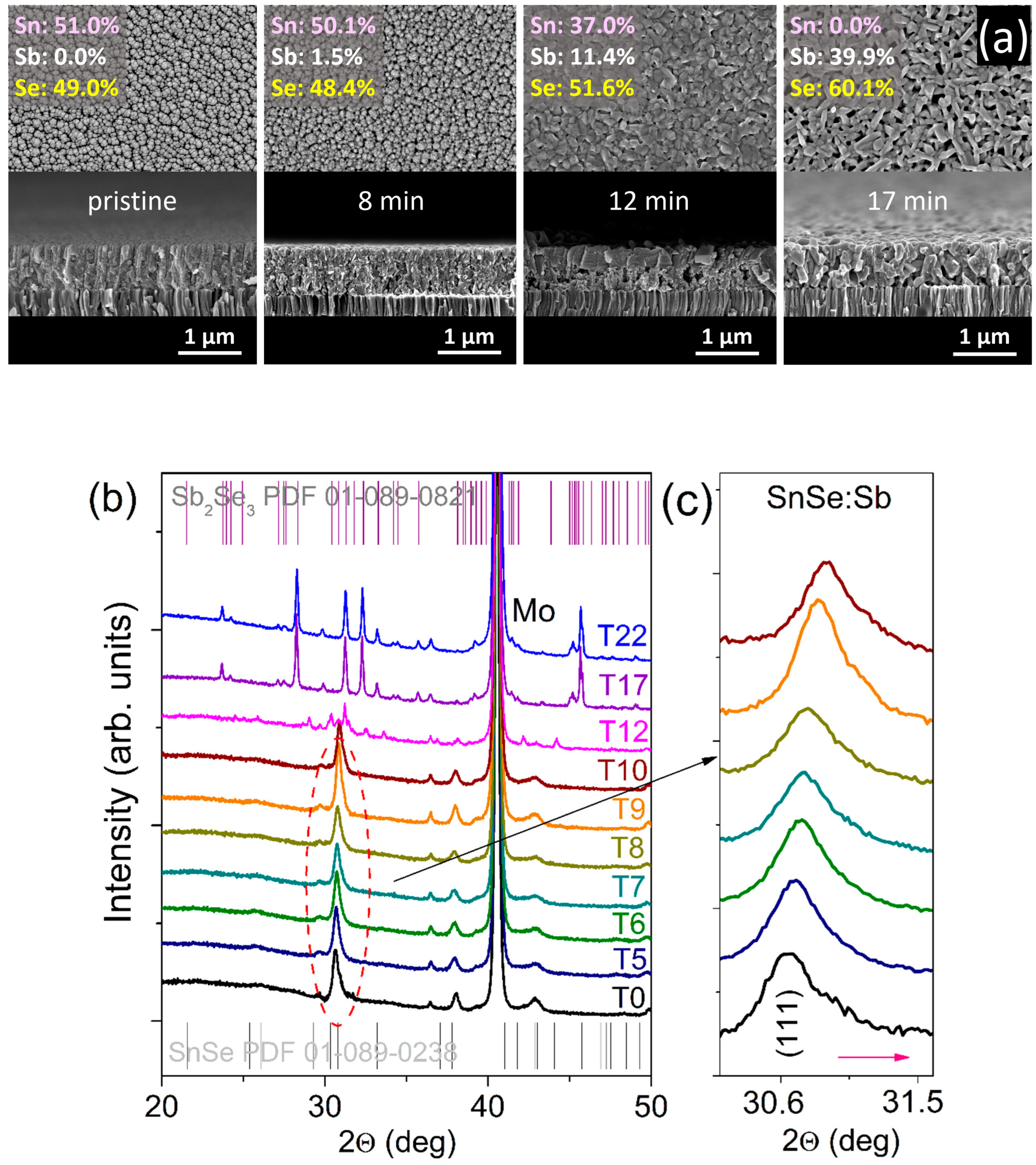
2.2.3. Time Treatment
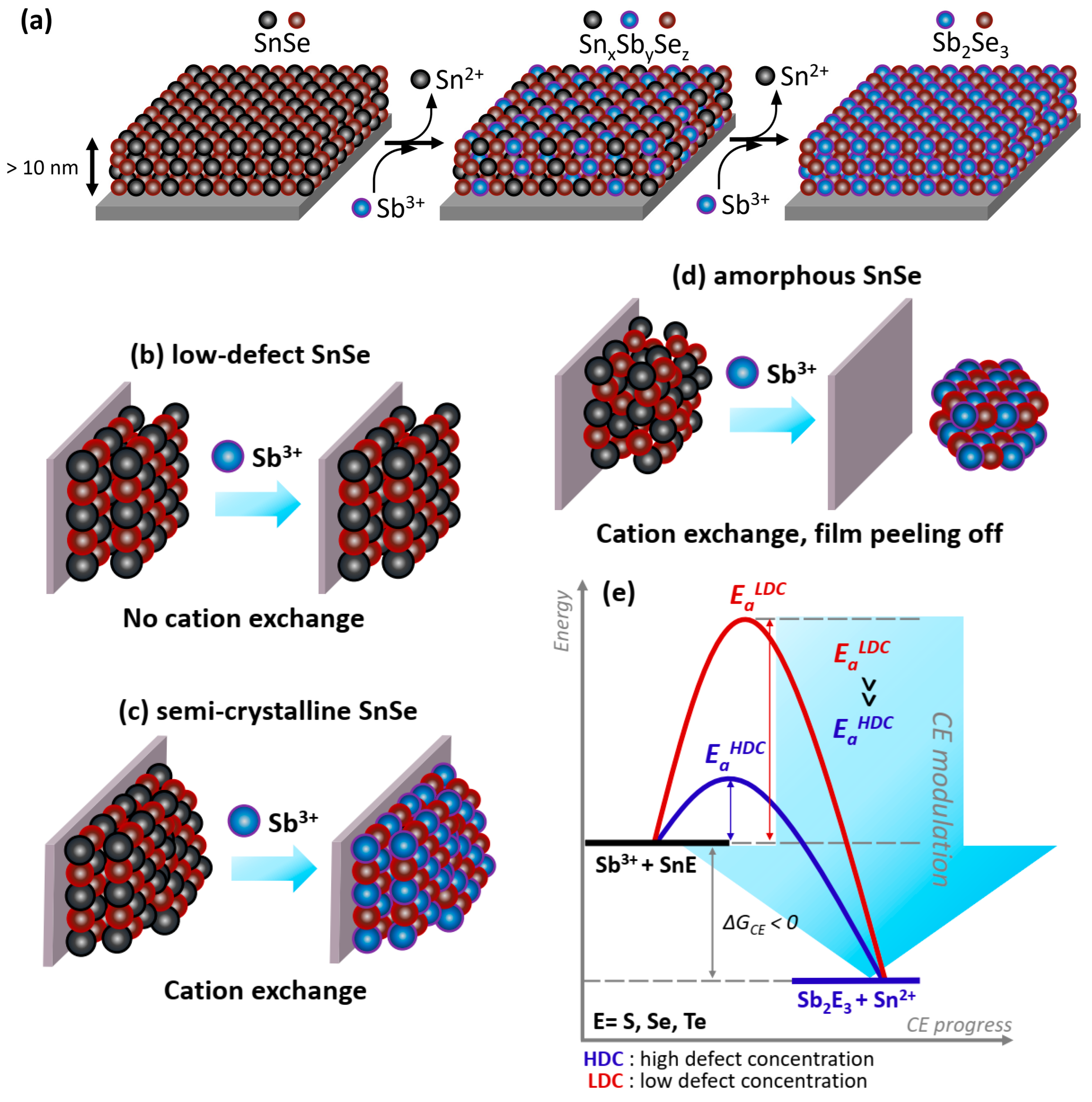
2.2.4. Discussion on the Ion-Exchange Mechanism
3. Summary
4. Methods
4.1. Template Film Fabrication
4.2. Ion Exchange
4.3. Characterization
4.4. Theoretical Calculation
4.5. DFT Calculation
Supplementary Materials
Author Contributions
Funding
Institutional Review Board Statement
Informed Consent Statement
Data Availability Statement
Conflicts of Interest
References
- Casavola, M.; van Huis, M.A.; Bals, S.; Lambert, K.; Hens, Z.; Vanmaekelbergh, D. Anisotropic Cation Exchange in PbSe/CdSe Core/Shell Nanocrystals of Different Geometry. Chem. Mater. 2012, 24, 294–302. [Google Scholar] [CrossRef]
- Justo, Y.; Sagar, L.K.; Flamee, S.; Zhao, Q.; Vantomme, A.; Hens, Z. Less Is More. Cation Exchange and the Chemistry of the Nanocrystal Surface. ACS Nano 2014, 8, 7948–7957. [Google Scholar] [CrossRef] [PubMed]
- Yalcin, A.O.; Fan, Z.; Goris, B.; Li, W.-F.; Koster, R.S.; Fang, C.-M.; van Blaaderen, A.; Casavola, M.; Tichelaar, F.D.; Bals, S.; et al. Atomic Resolution Monitoring of Cation Exchange in CdSe-PbSe Hetero-Nanocrystals during Epitaxial Solid-Solid-Vapor Growth. Nano Lett. 2014, 14, 3661–3667. [Google Scholar] [CrossRef]
- Bothe, C.; Kornowski, A.; Tornatzky, H.; Schmidtke, C.; Lange, H.; Maultzsch, J.; Weller, H. Solid-State Chemistry on the Nanoscale: Ion Transport through Interstitial Sites or Vacancies? Angew. Chem. Int. Ed. 2015, 54, 14183–14186. [Google Scholar] [CrossRef]
- Son, D.H.; Hughes, S.M.; Yin, Y.; Alivisatos, A.P. Cation Exchange Reactions in Ionic Nanocrystals. Science 2004, 306, 1009–1012. [Google Scholar] [CrossRef]
- Wu, H.-L.; Sato, R.; Yamaguchi, A.; Kimura, M.; Haruta, M.; Kurata, H.; Teranishi, T. Formation of Pseudomorphic Nanocages from Cu2O Nanocrystals Through Anion Exchange Reactions. Science 2016, 351, 1306–1310. [Google Scholar] [CrossRef]
- Steimle, B.C.; Fenton, J.L.; Schaak, R.E. Rational Construction of a Scalable Heterostructured Nanorod Megalibrary. Science 2020, 367, 418–424. [Google Scholar] [CrossRef]
- Li, Z.; Saruyama, M.; Asaka, T.; Tatetsu, Y.; Teranishi, T. Determinants of Crystal Structure Transformation of Ionic Nanocrystals in Cation Exchange Reactions. Science 2021, 373, 332–337. [Google Scholar] [CrossRef]
- Chen, H.; Cao, C.; Ge, B.; Li, Y.; Han, J.; Chen, Z. Wafer-Scale Metal Chalcogenide Thin Films Via an Ion Exchange Approach. J. Mater. Chem. C 2020, 8, 14393–14401. [Google Scholar] [CrossRef]
- Han, S.; Qin, X.; An, Z.; Zhu, Y.; Liang, L.; Han, Y.; Huang, W.; Liu, X. Multicolour Synthesis in Lanthanide-Doped Nanocrystals Through Cation Exchange in Water. Nat. Commun. 2016, 7, 13059. [Google Scholar] [CrossRef]
- Beberwyck, B.J.; Alivisatos, A.P. Ion Exchange Synthesis of III−V Nanocrystals. J. Am. Chem. Soc. 2012, 134, 19977–19980. [Google Scholar] [CrossRef] [PubMed]
- Moon, G.D.; Ko, S.; Xia, Y.; Jeong, U. Chemical Transformations in Ultrathin Chalcogenide Nanowires. ACS Nano 2010, 4, 2307–2319. [Google Scholar] [CrossRef] [PubMed]
- Goldstein, A.N.; Echer, C.M.; Alivisatos, A.P. Melting in Semiconductor Nanocrystals. Science 1992, 256, 1425–1427. [Google Scholar] [CrossRef] [PubMed]
- Polivtseva, S.; Adegite, J.O.; Kois, J.; Mamedov, D.; Karazhanov, S.Z.; Maricheva, J.; Volobujeva, O. A Novel Thermochemical Metal Halide Treatment for High-Performance Sb2Se3 Photocathodes. Nanomaterials 2021, 11, 52. [Google Scholar] [CrossRef] [PubMed]
- Li, Z.; Liang, X.; Li, G.; Liu, H.; Zhang, H.; Guo, J.; Chen, J.; Shen, K.; San, X.; Yu, W.; et al. 9.2%-Efficient Core-Shell Structured Antimony Selenide Nanorod Array Solar Sells. Nat. Commun. 2019, 10, 125. [Google Scholar] [CrossRef]
- Nam, K.-H.; Park, C.-M. 2D Layered Sb2Se3-Based Amorphous Composite for High-Performance Li- and Na-Ion Battery Anodes. J. Power Sources 2019, 433, 126639. [Google Scholar] [CrossRef]
- Pedrov, V.A.; Ganshin, V.A.; Korkishko, Y.N. Ion Exchange in 11-VI Crystals: Thermodynamics, Kinetics, and Technology. Phys. Status Solidi 1993, 139, 9. [Google Scholar]
- Polivtseva, S.; Spalatu, N.; Abdalla, A.; Volobujeva, O.; Hiie, J.; Bereznev, S. Pulsed Laser Deposition of Zn(O,Se) Layers for Optoelectronic Application. ACS Appl. Energy Mater. 2018, 1, 6505–6512. [Google Scholar] [CrossRef]
- Kois, J.; Polivtseva, S.; Mamedov, D.; Samieipour, A.; Karazhanov, S.Z. Visible Light-Assisted Instability of Kesterite Cu2ZnSnS4: What Are the Implications? Sol. Energy Mater. Sol. Cells 2020, 208, 110384. [Google Scholar] [CrossRef]
- Kois, J.; Polivtseva, S.; Bereznev, S. The Cost-Effective Deposition of Ultra-Thin Titanium (IV) Oxide Passivating Layers for Improving Photoelectrochemical Activity of SnS Electrodes. Thin Solid Film. 2019, 671, 152–156. [Google Scholar] [CrossRef]
- Kumar, A.; Kumar, V.; Romeo, A.; Wiemer, C.; Mariotto, G. Raman Spectroscopy and In Situ XRD Probing of the Thermal Decomposition of Sb2Se3 Thin Films. J. Phys. Chem. C 2021, 125, 19858–19865. [Google Scholar] [CrossRef]
- Yang, W.; Kim, J.H.; Hutter, O.S.; Phillips, L.J.; Tan, J.; Park, J.; Lee, H.; Major, J.D.; Lee, J.S.; Moon, J. Benchmark performance of low-cost Sb2Se3 photocathodes for unassisted solar overall water splitting. Nat. Commun. 2020, 11, 861. [Google Scholar] [CrossRef] [PubMed]
- Oueslati, S.; Kauk-Kuusik, M.; Neubauer, C.; Mikli, V.; Meissner, D.; Brammertz, G.; Vermang, B.; Krustok, J.; Grossberg, M. Study of (AgxCu1−x)2ZnSn(S,Se)4 Monograins Synthesized by Molten Salt Method for Solar Cell Applications. Sol. Energy 2020, 198, 586–595. [Google Scholar] [CrossRef]
- Oueslati, S.; Grossberg, M.; Kauk-Kuusik, M.; Mikli, V.; Ernits, K.; Meissner, D.; Krustok, J. Effect of Germanium Incorporation on the Properties of Kesterite Cu2ZnSn(S,Se)4 Monograins. Thin Solid Film. 2019, 669, 315–320. [Google Scholar] [CrossRef]
- Kauk-Kuusik, M.; Timmo, K.; Muska, K.; Pilvet, M.; Krustok, J.; Josepson, R.; Brammertz, G.; Vermang, B.; Danilson, M.; Grossberg, M. Detailed Insight into the CZTS/CdS Interface Modification by Air Annealing in Monograin Layer Solar Cells. ACS Appl. Energy Mater. 2021, 4, 12374–12382. [Google Scholar] [CrossRef]
- Available online: http://www.wiredchemist.com/chemistry/data/metallic-radii (accessed on 1 July 2022).
- Shannon, R.D. Revised Effective Ionic Radii and Systematic Studies of Interatomic Distances in Halides and Chalcogenides. Acta Cryst. 1976, A32, 751–767. [Google Scholar] [CrossRef]
- Wang, Z.-L.; Xie, W.-H.; Zhao, Y.-H. Tunable Band Structure and Effective Mass of Disordered Chalcopyrite. Front. Phys. 2017, 12, 127103. [Google Scholar] [CrossRef]
- Liu, C.-Y.; Li, Z.-M.; Gu, H.-Y.; Chen, S.-Y.; Xiang, H.; Gong, X.-G. Sodium Passivation of the Grain Boundaries in CuInSe2 and Cu2ZnSnS4 for High-Efficiency Solar Cells. Adv. Energy Mater. 2017, 7, 1601457. [Google Scholar] [CrossRef]
- Sun, J.; Yu, J.; Guo, Y.; Wang, Q. Enhancing Power Factor of SnSe Sheet with Grain Boundary by Doping Germanium or Silicon. Npj Comput. Mater. 2020, 6, 99. [Google Scholar] [CrossRef]
- Li, Y.; Wu, H.; Qi, W.; Zhou, X.; Li, J.; Cheng, J.; Zhao, Y.; Li, Y.; Zhang, X. Passivation of Defects in Perovskite Solar Cell: From a Chemistry Point of View. Nano Energy 2020, 77, 105237. [Google Scholar] [CrossRef]
- Fan, Z.; Lin, L.-C.; Buijs, W.; Vlugt, T.J.H.; van Huis, M.A. Atomistic Understanding of Cation Exchange in PbS Nanocrystals Using Simulations with Pseudoligands. Nat. Commun. 2016, 7, 11503. [Google Scholar] [CrossRef] [PubMed]
- Ismailova, E.N.; Mashadieva, L.F.; Babanly, D.M.; Shevel’kov, A.V.; Babanly, M.B. Diagram of Solid-Phase Equilibria in the SnSe–Sb2Se3–Se System and Thermodynamic Properties of Tin Antimony Selenides. Russ. J. Inorg. Chem. 2021, 66, 96–103. [Google Scholar] [CrossRef]
- Kresse, G.; Furthmüller, J. Efficiency of Ab-initio Total Energy Calculations for Metals and Semiconductors Using a Plane-Wave Basis Set. Comput. Mater. Sci. 1996, 6, 15–50. [Google Scholar] [CrossRef]
- Kresse, G.; Furthmüller, J. Efficient Iterative Schemes for Ab-initio Total-Energy Calculations Using a Plane-Wave Basis Set. Phys. Rev. B 1996, 54, 11169. [Google Scholar] [CrossRef]
- Blöchl, P.E. Projector Augmented-Wave Method. Phys. Rev. B 1994, 50, 17953–17979. [Google Scholar] [CrossRef]
- Kresse, G.; Joubert, D. From Ultrasoft Pseudopotentials to the Projector Augmented-Wave Method. Phys. Rev. B 1999, 59, 1758. [Google Scholar] [CrossRef]
- Perdew, J.P.; Burke, K.; Ernzerhof, M. Generalized Gradient Approximation Made Simple. Phys. Rev. Lett. 1996, 77, 3865–3868. [Google Scholar] [CrossRef]
- Henkelman, G.; Arnaldsson, A.; Jónsson, H. A fast and robust algorithm for Bader decomposition of charge density. Comput. Mater. Sci. 2006, 36, 354–360. [Google Scholar] [CrossRef]


Publisher’s Note: MDPI stays neutral with regard to jurisdictional claims in published maps and institutional affiliations. |
© 2022 by the authors. Licensee MDPI, Basel, Switzerland. This article is an open access article distributed under the terms and conditions of the Creative Commons Attribution (CC BY) license (https://creativecommons.org/licenses/by/4.0/).
Share and Cite
Polivtseva, S.; Kois, J.; Kruzhilina, T.; Kaupmees, R.; Klopov, M.; Molaiyan, P.; van Gog, H.; van Huis, M.A.; Volobujeva, O. Solution-Mediated Inversion of SnSe to Sb2Se3 Thin-Films. Nanomaterials 2022, 12, 2898. https://doi.org/10.3390/nano12172898
Polivtseva S, Kois J, Kruzhilina T, Kaupmees R, Klopov M, Molaiyan P, van Gog H, van Huis MA, Volobujeva O. Solution-Mediated Inversion of SnSe to Sb2Se3 Thin-Films. Nanomaterials. 2022; 12(17):2898. https://doi.org/10.3390/nano12172898
Chicago/Turabian StylePolivtseva, Svetlana, Julia Kois, Tatiana Kruzhilina, Reelika Kaupmees, Mihhail Klopov, Palanivel Molaiyan, Heleen van Gog, Marijn A. van Huis, and Olga Volobujeva. 2022. "Solution-Mediated Inversion of SnSe to Sb2Se3 Thin-Films" Nanomaterials 12, no. 17: 2898. https://doi.org/10.3390/nano12172898