1. Introduction
In micro-electromechanical systems (MEMS) devices, especially MEMS resonators, AlN material has great potential due to the excellent acoustic properties, piezoelectric properties, and good compatibility with other microelectronic technologies. The performance of MEMS resonators depends on the quality of piezoelectric films, especially the piezoelectric property. This is typically characterized by piezoelectric coefficients or electromechanical coupling coefficient k in various modes. The latter is usually measured for SAW (surface acoustic wave) devices. It can be calculated by the piezoelectric coefficients, elastic, and dielectric constants in corresponding modes. Thus, the piezoelectric coefficients are the base to characterize the piezoelectric property. AlN has three independent piezoelectric coefficients d31, d15, and d33. Among them, the piezoelectric coefficient d33 is commonly used to characterize the piezoelectric property based on its feasibility and simplicity.
There are many methods to determine the piezoelectric coefficient quantitatively, such as the Berlincourt method [
1], capacitance measurement [
2,
3], laser interferometer [
4,
5,
6,
7], and piezoresponse force microscopy (PFM) method [
8,
9,
10,
11,
12]. Among these methods, the Berlincourt method is a standard method to determine the piezoelectric properties. It is feasible for bulk material with rather high coefficients, such as PZT. For AlN thin films, however, this is difficult to implement. The principle of capacitance measurement is to describe the deformation of thin films by the variation of the sample’s capacitance. The piezoelectric films act as the dielectric layers. This is limited by the low precision and the influence of the interfacial capacitance between the electrodes and piezoelectric films. For laser interferometry, it needs a FEM simulation as a supplementary to obtain the results and the local heating remains unsolved. The PFM measurement used in the paper, which is based on the converse piezoelectric effect, is a direct and effective measurement method. Any points on the piezoelectric films can be detected specifically. The measurement results are essentially effective values which are always smaller than the actual coefficient due to the substrate constraints [
11]. There are many different measurement values of AlN thin films reported in the literature, however, it is difficult to make a fair comparison between them as they all ignore the influences of the substrate and electric field distribution. The testing values of the films prepared in the same conditions may even be different under different structural constraints, electric field distribution, thickness, and test configurations. The actual d
33 of the AlN films is very important for the design and performance optimization of MEMS devices. It is necessary to find a way to eliminate the effect of the constraints and extract the actual d
33 of AlN thin films. Few systematical studies on this aspect were reported.
In our work, two different AlN samples, namely a sample with a top electrode and one without a top electrode, were measured by PFM to study the influence of electric field distribution. To calculate the numerical solution, a theoretical analysis was implemented and an equivalent model for the PFM testing system was built by FEM simulation. The effects of electric field distribution and substrate constraints to the measurement results were analyzed systematically by simulation.
By comparing experimental results of AlN films with the values calculated by FEM, a novel and effective method to extract the actual piezoelectric coefficient d33 was given. Contrasting with the values reported in the literature, the values in the paper were theoretically rational. Due to a good agreement between the extracted values d33 of two different samples made from the same wafer, the accuracy and rationality of the method were verified.
2. Experimental Section
Due to the smaller lattice mismatch and the close thermal expansion coefficient, the AlN thin films deposited on the Pt/Ti layers exhibit good c-axis orientation [
13]. Consequently, the layers of Ti (60 nm) and Pt (60 nm) were deposited as the bottom electrode on the 500 μm-thick n-type (100) Si substrate sequentially. The Ti layer was used to promote the adhesion of the Pt electrode. The c-axis textured AlN thin film with a thickness of 450 nm was then deposited on the Pt layer. AlN film was prepared by reactive magnetron sputtering with a pure Al target in an Ar/N
2 atmosphere.
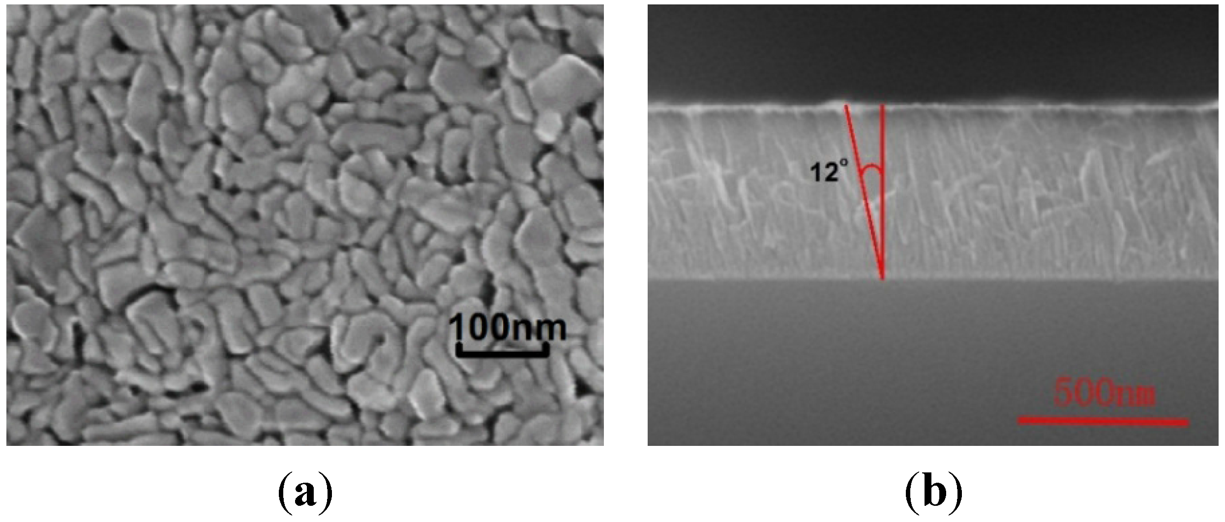
Prior to the PFM measurement, the properties of AlN polycrystalline thin films, including the surface roughness, grain size, morphology, and the (002) crystal orientation were characterized. The root-mean-square (RMS) surface roughness of the AlN thin film was 3.2 nm under a scanning range of 5 μm × 5 μm, determined by atomic force microscope (AFM) in tapping mode. The grain size and morphology of the AlN film were measured by a scanning electron microscope (SEM), as seen in
Figure 1.
Figure 1a showed the grain size of the AlN polycrystalline film is approximately 40–50 nm, which indicated fine grains and good compactness. A cross-section of the AlN film with the typical c-axis which is oriented nearly perpendicular to the substrate can be seen in
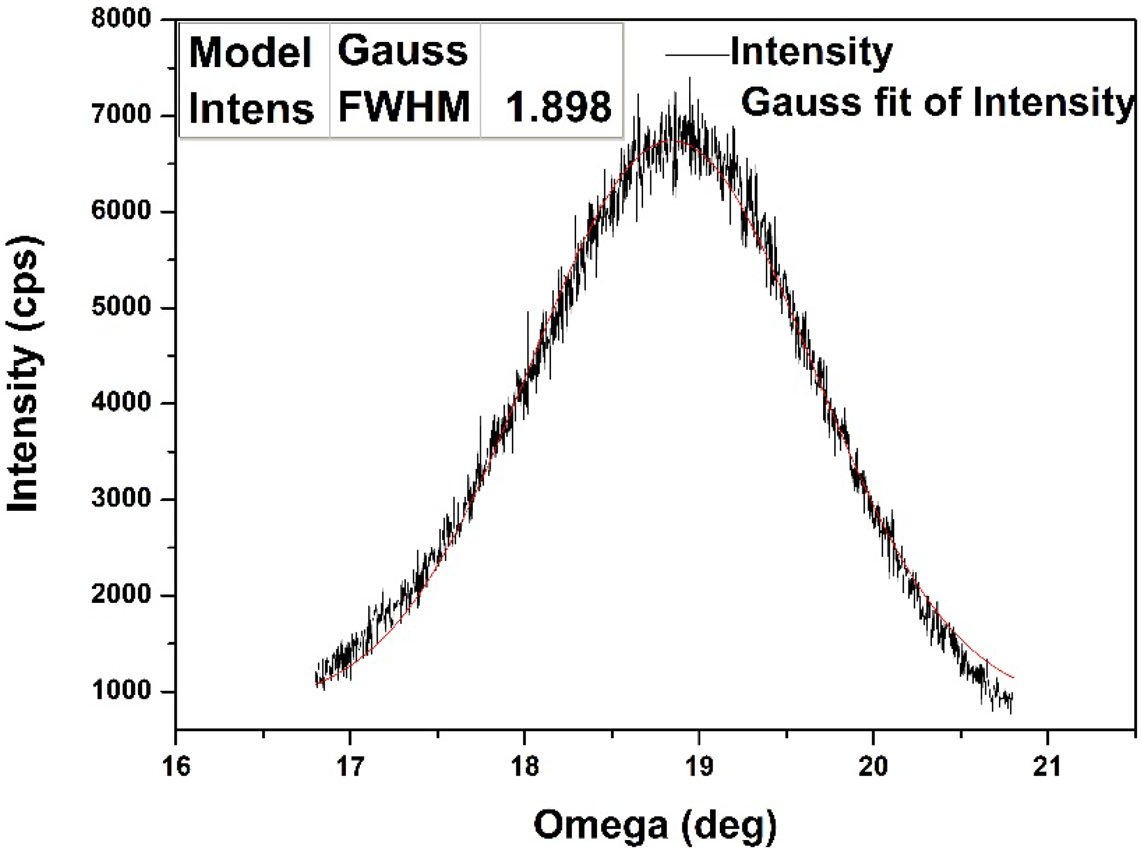
Figure 1b. The full width of half maximum (FWHM) of the rocking curve was measured by X-ray diffraction (XRD) to assess, quantitatively, the preferred (002) orientation as shown in
Figure 2. Generally, a (002)-oriented AlN film with the FWHM less than 4° is the precondition of good piezoelectric property [
14]. The FWHM of the rocking curve around (002) orientation for the AlN sample was about 1.9°, which meant the AlN thin film has a good piezoelectric property.
To characterize the piezoelectric properties of AlN films directly and effectively, the piezoelectric coefficient d33 was determined by PFM. PFM measurement is based on the converse piezoelectric effect of piezoelectric films. An excitation voltage is applied onto the surface of the film by the conducting probe of the PFM. The deformation of the film induced by the electric field can be detected by the probe. Then, the piezoelectric coefficient can be obtained.
The external excitation voltage can be imposed between the probe and the bottom electrode or between the top and bottom electrodes on the substrate. The electric field in the AlN thin films is inhomogeneous for the former while it is homogenous for the latter. To investigate the influence of electric field distribution to the deformation, two samples with different electric configurations were characterized. They were made from the same wafer, which meant the AlN polycrystalline film was deposited under the same conditions. The bottom electrode Pt was exposed by lithography, followed by inductively-coupled plasma (ICP) dry etching of AlN. One section of the wafer was patterned with the top electrode Al on AlN thin film through lift-off technology while the other one was left untreated. By comparing the measurement results of the two samples, the influence by electric field distribution to the measurement could be analyzed.
The testing schematics of the experimental samples are shown in
Figure 3. The bias voltage was applied on the top surface of AlN thin film or the top electrode through the PFM probe with contacting mode. The Pt bottom electrode was connected to the ground by gold wire. Then the piezoelectric test loop was achieved. When an AC modulation signal was applied on to the top surface, the deformation signal induced by piezoelectric effect could be detected by a photodetector and the lock-in amplifier. A piezoelectric strain curve could be recorded to determine the piezoelectric coefficient, quantitatively.
Figure 1.
(a) The surface morphology of AlN film; and (b) The cross-section of sample.
Figure 1.
(a) The surface morphology of AlN film; and (b) The cross-section of sample.
Figure 2.
The rocking curve for (002) orientation of AlN polycrystalline thin films.
Figure 2.
The rocking curve for (002) orientation of AlN polycrystalline thin films.
Figure 3.
The testing schematics of the experimental samples, (a) the sample without the top electrode and (b) the sample with the top electrode.
Figure 3.
The testing schematics of the experimental samples, (a) the sample without the top electrode and (b) the sample with the top electrode.
3. Theoretical Analysis and Numerical Solution
A theoretical calculation about the deformation of AlN thin film in the experiment is given. The constitutive equations of the piezoelectric effect are given [
15]:
where
is the strain matrix,
is the compliance matrix at constant electric field,
is the stress,
is the piezoelectric coefficient matrix,
is the applied electric field,
is the displacement and
is the permittivity at constant stress.
Considering the elastic mechanics and piezoelectric effect, the strain
in the electric field region can be calculated as Equation (1) while the strain
out of the electric field region can be calculated as follows:
The constraints and boundary conditions based on the experimental system are as follows:
(i) Stress boundary conditions: except the bottom surface of AlN films, the values of stress on other free surfaces are zero.
(ii) Displacement boundary conditions: the displacement of the bottom surface is zero, due to the constraints by the substrate.
(iii) The values of voltage: the voltage applied in the electric region on the top surface is 7 V and the bottom surface of AlN thin film which is connected to Pt bottom electrode is 0 V.
(iv) Continuity conditions for displacement: the displacements at the boundary between electric region and non-electric region are the same.
To solve the displacement equations, the strain should be replaced by Equations (1) and (3). With the boundary conditions above, the equations can be solved, in theory, to obtain the displacements; however, to solve the tensor equations is extremely complex. Thus, the displacement functions are difficult to work out. Then, the finite element method (FEM) was used to calculate a numerical solution of displacement due to its simplicity.
To conform to the actual testing conditions, the equivalent model of piezoelectric measurement system was simplified and established by FEM simulation as follows:
(i) For the sample without top electrode, the voltage was applied on the top surface of AlN through the PFM probe in the experiment. Thus, in the equivalent model the voltage in a circle with the probe’s radius of 30 nm as the electric region was set as 7 V. The circle could be set at the center of AlN top surface. For the sample with a top electrode covering 2/3 of the area of film, the voltage in a square with a side length of 2 μm was set as 7 V.
(ii) Since the Pt electrode was connected to ground, the voltage of the AlN bottom surface could be set as 0 V in the model.
(iii) The AlN film was firmly clamped to a considerably thick substrate and the substrate was stuck to a rigid holder in the experiment. Hence, the bottom surface was assumed to be fixed and other surfaces of the structure were set free.
(iv) The in-plane dimension of the AlN sample was 2000 μm × 2000 μm, which was far larger than the PFM probe size. Considering the dimensions and the visualization, the in-plane size of film was set 3 μm × 3 μm, which was two orders of magnitude larger than the PFM probe size. The thickness of the model was set 450 nm, the same as the actual AlN sample.
The continuity conditions for displacement and the piezoelectric effect were also taken into account in the simulation. The piezoelectric constants were set as d33-theory = 5.4901 pm/V, d31-theory = −2.7813 pm/V, and d15-theory = 3.8400 pm/V, which were the intrinsic values of the AlN material applied in the simulation. According to the conditions described above, an equivalent model could be established and the surface deformation induced by piezoelectric effect could be calculated.
4. Results and Discussion
4.1. Simulation Results
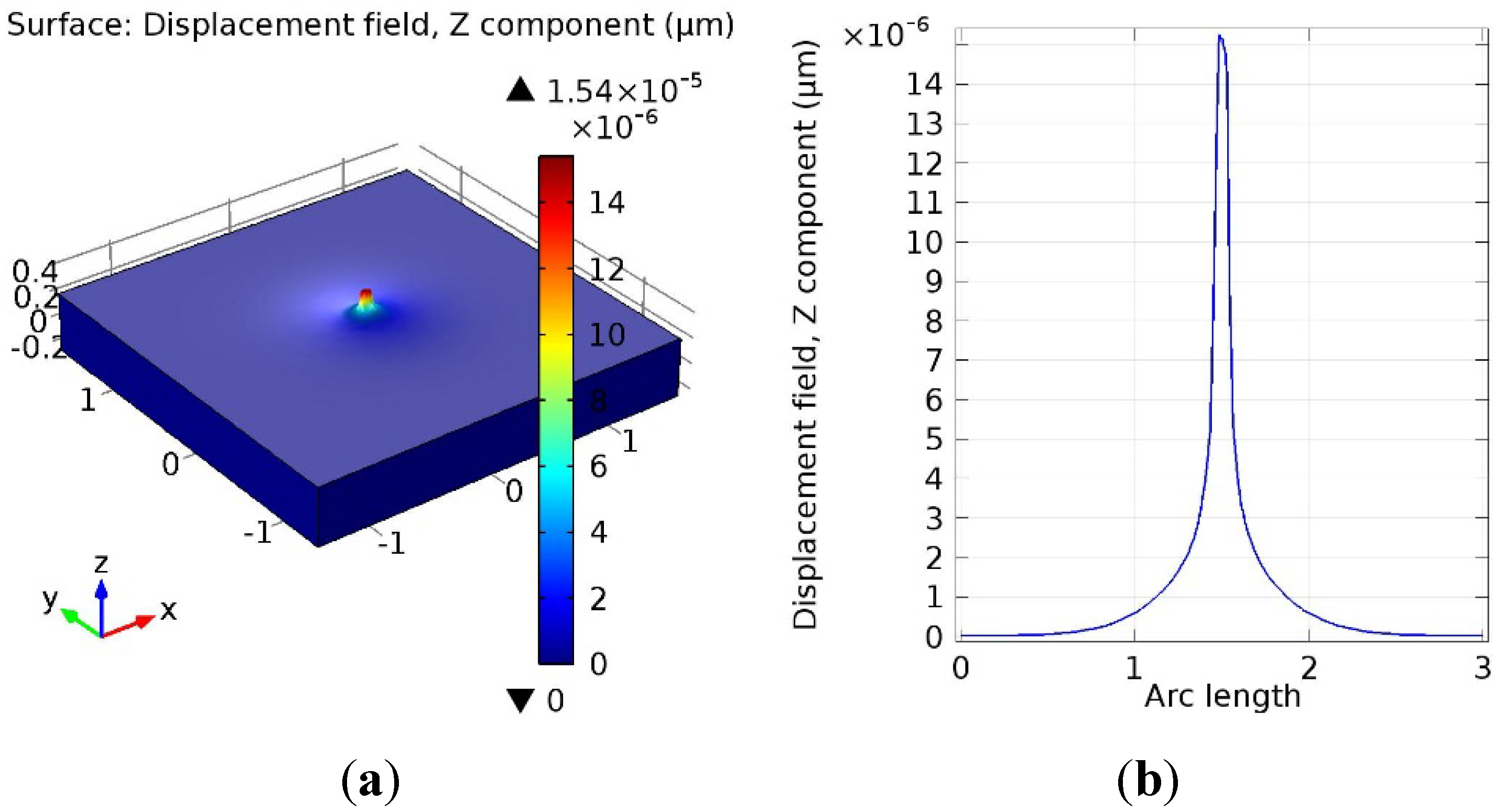
The simulation results for the sample without top electrode are shown in the
Figure 4. A three-dimensional figure for surface deformation of the AlN film is shown in
Figure 4a. It can be observed that the deformation region of film is mainly near the probe region which matches the practical case.
Figure 4b shows the
z-axis displacement along the center line across the top surface. In the probe region, the maximum displacement is 15.4 pm at the voltage of 7 V. The coefficient in the equivalent model d
33-model is calculated as 2.2000 pm/V directly.
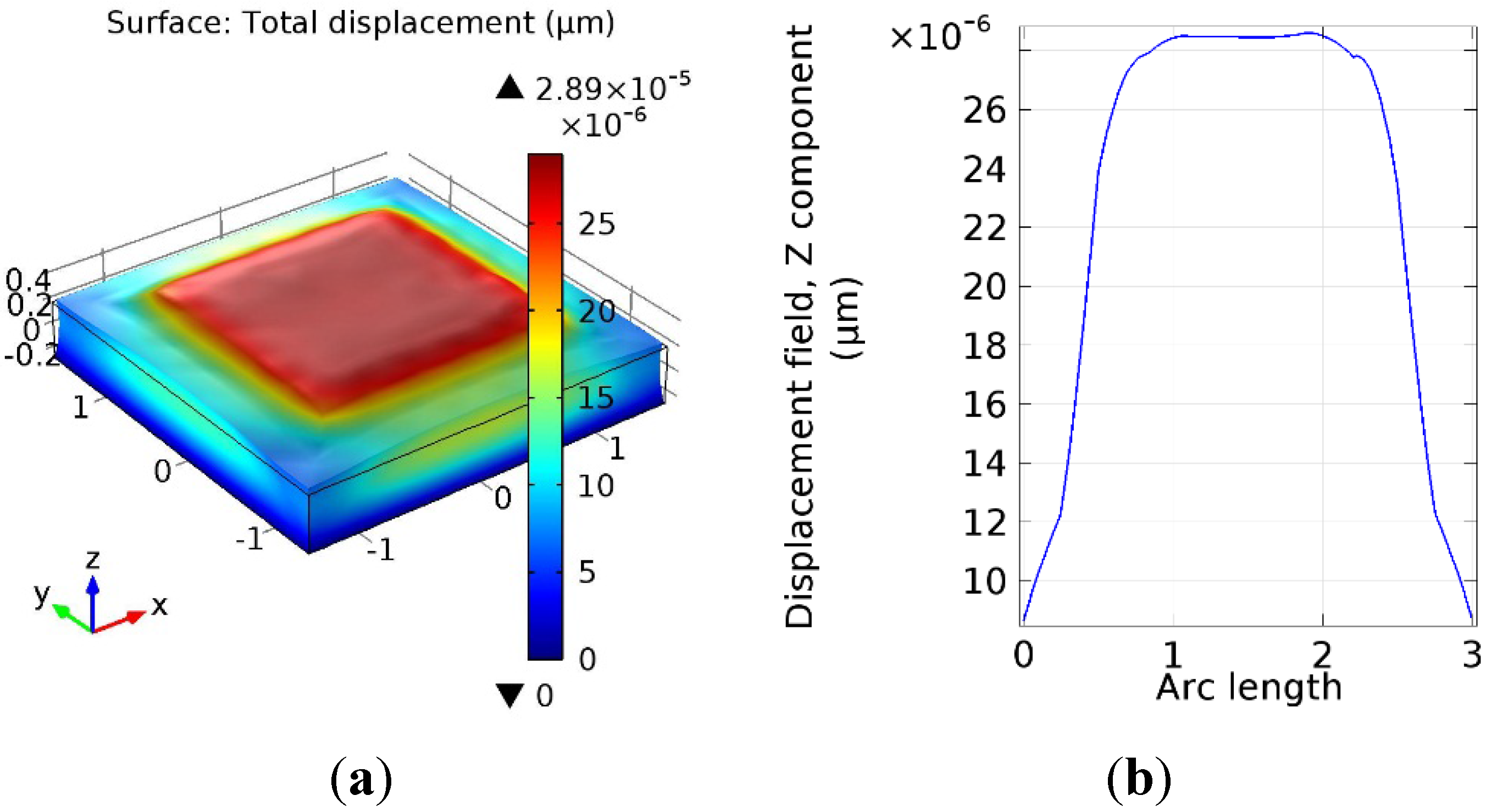
At the same time, the simulation was also performed for the sample with a top electrode, as shown in
Figure 5. The voltage of 7 V was applied on the square region and caused the deformation of 28.9 pm in the electric region. The piezoelectric coefficient can be calculated as 4.1286 pm/V. The two equivalent models are the same except the electric field distribution. By comparing the two results, the influence of the electric field distribution can be analyzed. It is clear that the structure with a top electrode shows a larger deformation in the electric region under the same excitation voltage. This indicates that the deformation of the top surface increases as the size of top electrode increases, which is in good accordance with previous reports [
6,
16]. The results can be explained by the contribution of the dipoles inside the piezoelectric films. The external electric field makes the dipoles point in a certain direction. The highest piezoelectric value can be reached when all the dipoles have the same contribution to the deformation of the top surface [
8]. As the size of top electrode increases, the number of the dipoles involved increases. Then, the deformation of the films increases. Thus, the electric field distribution should be taken into consideration to determine the piezoelectric coefficient.
Figure 4.
The simulation results for the sample without a top electrode; (a) a three-dimensional figure of the surface deformation and (b) the z-axis displacement along the center line at 7 V.
Figure 4.
The simulation results for the sample without a top electrode; (a) a three-dimensional figure of the surface deformation and (b) the z-axis displacement along the center line at 7 V.
Figure 5.
The simulation results for the sample with a top electrode; (a) a three-dimensional figure of the surface deformation and (b) the z-axis displacement along the center line at 7 V.
Figure 5.
The simulation results for the sample with a top electrode; (a) a three-dimensional figure of the surface deformation and (b) the z-axis displacement along the center line at 7 V.
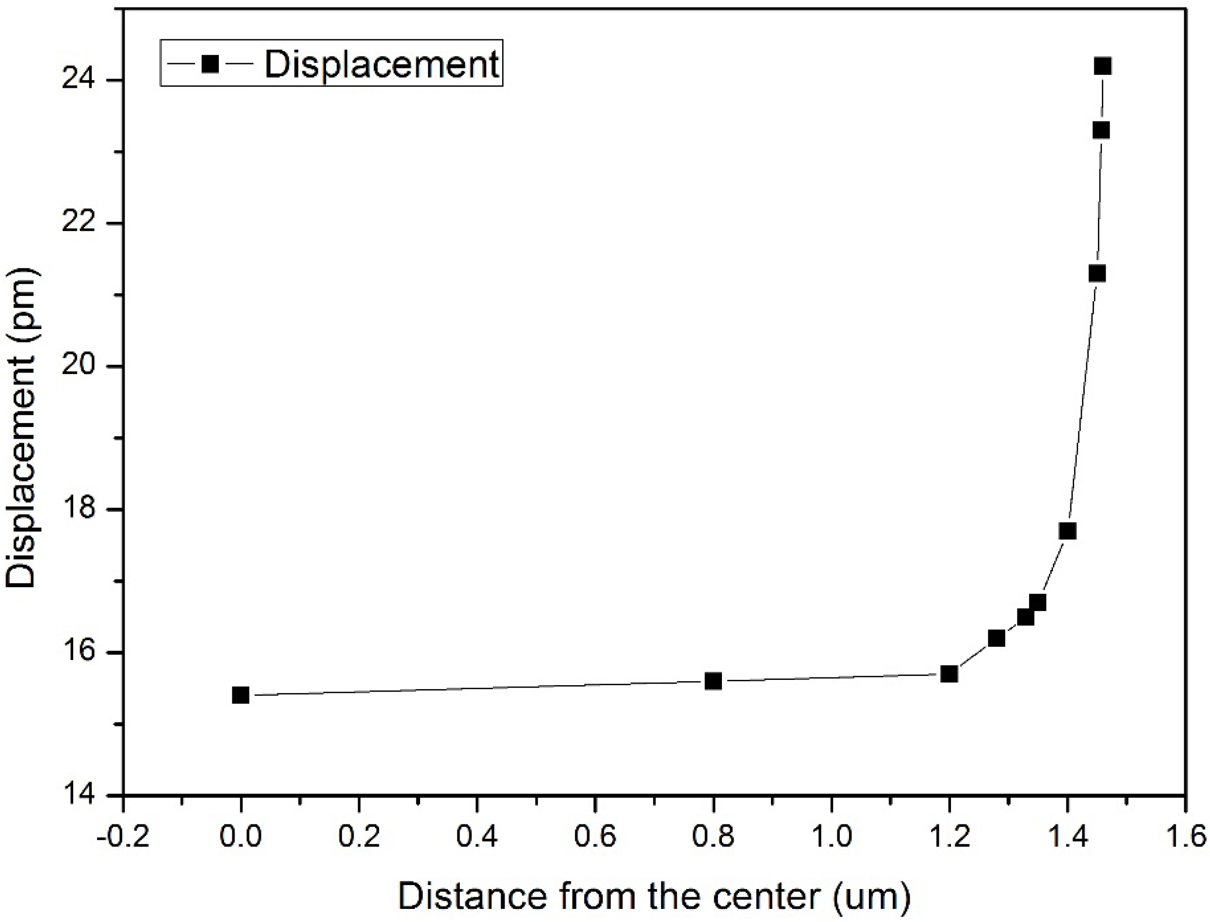
In addition, some other points along the
x-axis from the center to the edge were also simulated under the same constraints for the sample without a top electrode. The results are shown in
Table 1 and plotted in
Figure 6. They demonstrate that the closer to the edge, the larger the displacement. In particular, the displacements induced by the external voltage increase slightly as the simulated points are not near the edge while the displacements increase rapidly near the edge. The in-plane stress induced by d
31 [
16] should be considered for the interpretation of the changes of the displacements. The in-plane stress is very asymmetrical in the
x-axis direction for the points near the edge and it results in the rapid increase of displacements near the edge.
Table 1.
The simulation results along with the distance from the center.
Table 1.
The simulation results along with the distance from the center.
| Variables | Numerical Values |
|---|
| Distance from the Center (μm) | 0 | 0.8 | 1.2 | 1.28 | 1.33 | 1.35 | 1.4 | 1.45 | 1.457 | 1.46 |
| Displacement at the Voltage of 7 V (pm) | 15.4 | 15.6 | 15.7 | 16.2 | 16.5 | 16.7 | 17.7 | 21.3 | 23.3 | 24.2 |
Figure 6.
The displacements change with the distance from the center.
Figure 6.
The displacements change with the distance from the center.
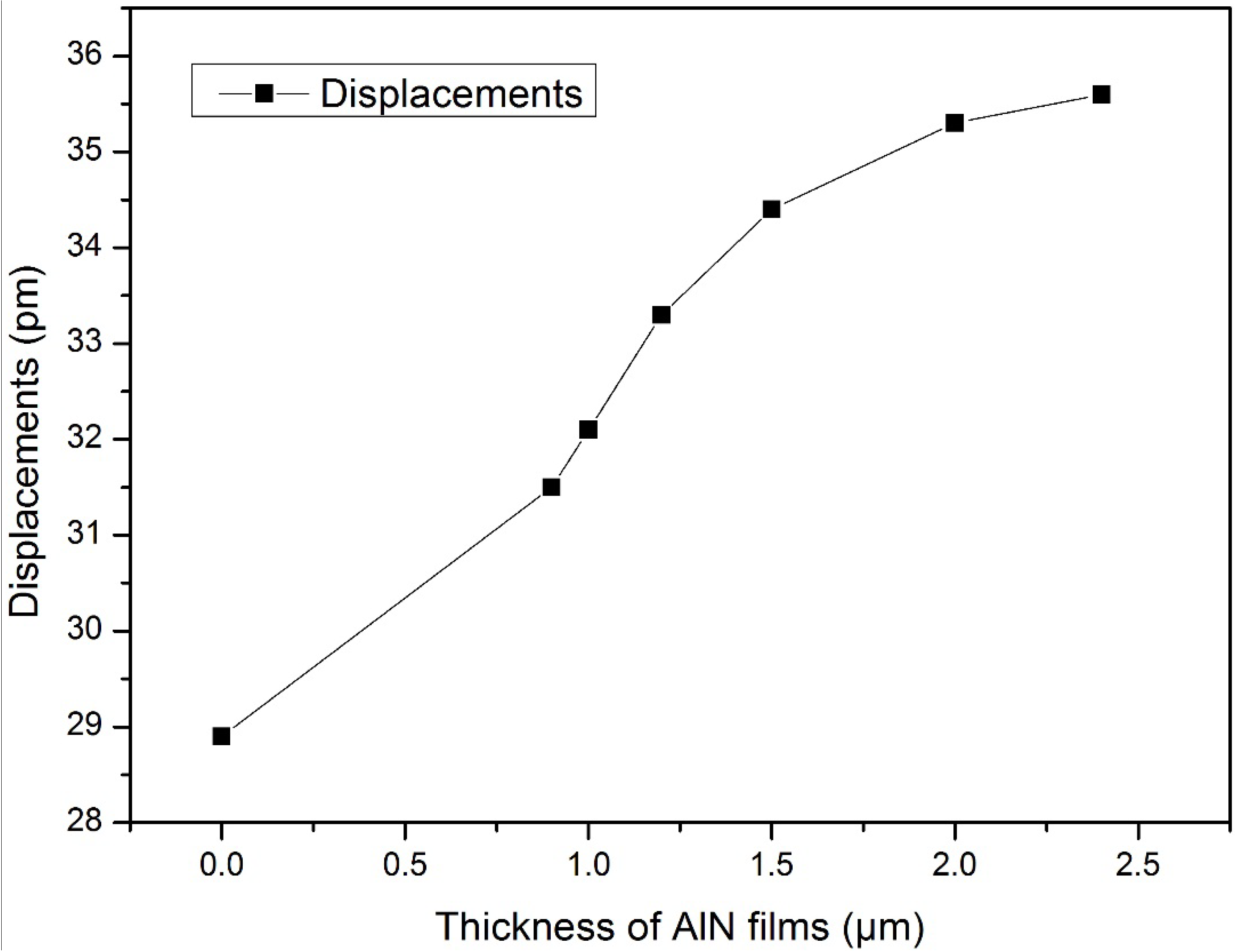
For the test configuration with the top electrode, AlN films with different thicknesses were also simulated. The results are shown in the
Table 2 and plotted in
Figure 7. They indicate that under the same external voltage of 7 V, the displacements increase with the increase of thickness, which is in good accordance with the reports in the literature [
4,
7]. Ababneha attributed this to the increasing self-heating effect which caused lower defects in films [
4]. Moreover, for the films in the simulation without considering the defects, the substrate constraints give rise to the results. When the thickness is 2.4 μm, the piezoelectric coefficient d
33 can be calculated as 5.0857 pm/V, which is close to the value of bulk material. The impacts of substrate constraints to the displacements become smaller as the thickness increases. Consequently, the contribution of substrate constraints were different for AlN films with different thicknesses. This was often neglected in the measurement and obtained inaccurate results.
Table 2.
The displacements for different thicknesses for the configuration with the top electrode.
Table 2.
The displacements for different thicknesses for the configuration with the top electrode.
| Variables | Numerical Values |
|---|
| Thickness of Films (μm) | 0.45 | 0.9 | 1 | 1.2 | 1.5 | 2 | 2.4 |
| Displacement at the Voltage of 7 V (pm) | 28.9 | 31.5 | 32.1 | 33.3 | 34.4 | 35.3 | 35.6 |
Figure 7.
The displacements change with the thickness of AlN films.
Figure 7.
The displacements change with the thickness of AlN films.
In a word, the electric field distribution, thickness, and substrate constraints all influence the final displacements. The reasons have been analyzed above. From the simulation, it is also demonstrates that the simulated values under the equivalent constraints are both smaller than the intrinsic value 5.4901 pm/V of AlN material. The substrate confines the motion of AlN thin films and the electric field distribution confines the deformation range of films. According to this, the measurement results d33-test would be smaller than the intrinsic piezoelectric coefficient d33 of an actual AlN sample. The rationality of the equivalent model have been verified by the accordance between the simulation results and the reports in previous literatures.
4.2. Experimental Results
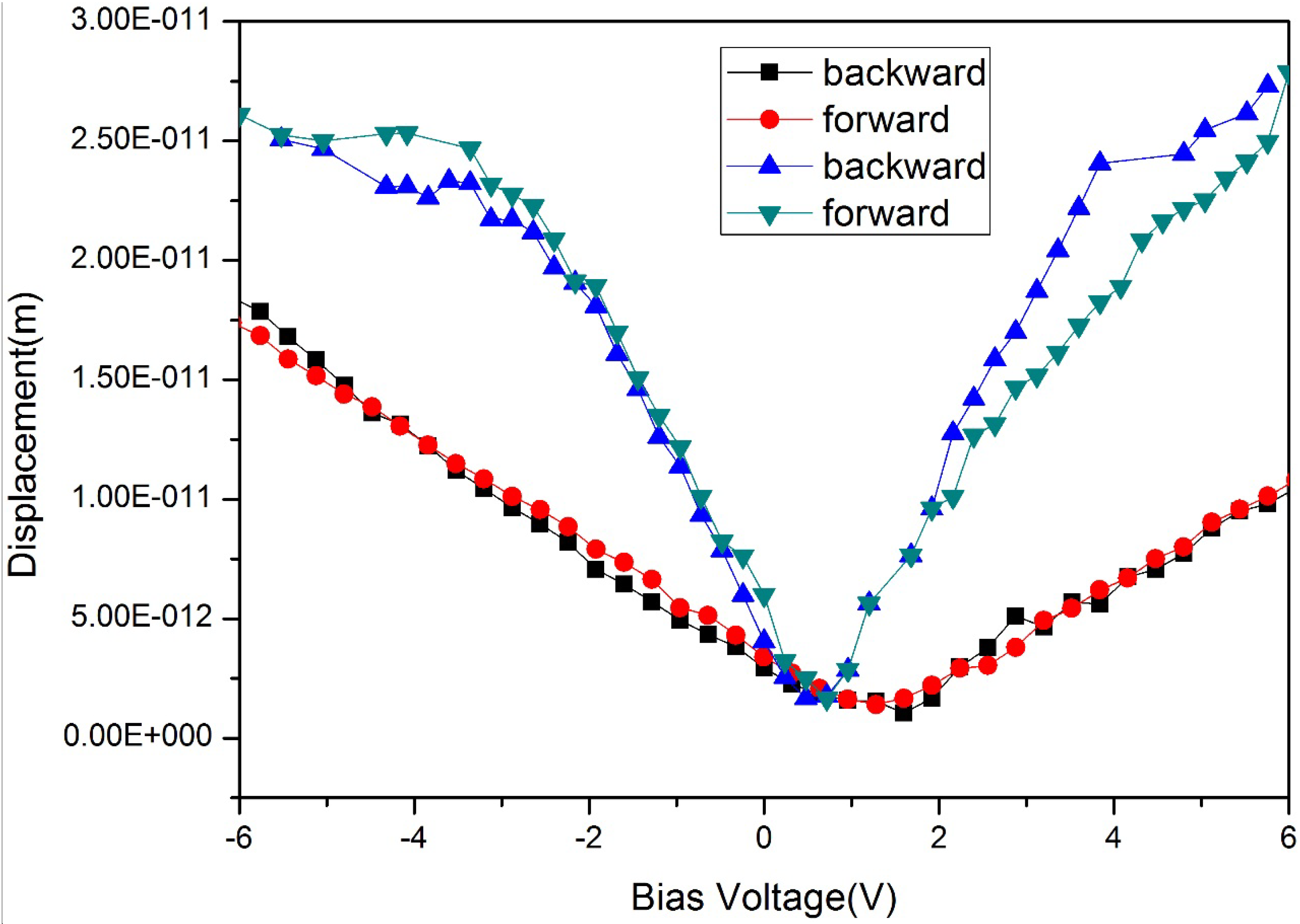
The bidirectional test mode of PFM was used with the voltage ranging from −6 to 6 V in the experiments. The curves in
Figure 8 show the relation between displacements of the top surface and the bias voltage obtained in the PFM measurement. For each sample, two testing curves for forward scanning and backward scanning are given. From the slope of the piezoelectric strain curves, effective values d
33-test for two different samples are obtained as 2.0421 and 3.8071 pm/V, respectively. The measurement values are close to the simulation values for corresponding structures. The measurement value of 2.0421 pm/V for the sample without a top electrode is smaller than the value of 3.8071 pm/V for the other sample. This is in agreement with the simulation results. Furthermore, some other points on the surface of the sample without a top electrode were also detected. The displacements at the voltage of 7 V were 14.30, 14.69, 16.03, 21.84, and 23.00 pm from the center to the edge. The change law of displacements in the experiment is in accordance with the simulation results. The experimental results support the simulation well and the rationality and accuracy of the equivalent model are verified.
Figure 8.
The piezoelectric strain curves obtained in the measurement; the black and red curves are for the sample without a top electrode, and the green and blue curves are for the sample with a top electrode.
Figure 8.
The piezoelectric strain curves obtained in the measurement; the black and red curves are for the sample without a top electrode, and the green and blue curves are for the sample with a top electrode.
According to the theoretical analysis and simulation results, the coefficients calculated in the experiment were effective values under the substrate constraints and non-ideal electric field distribution. They could not represent the actual piezoelectric coefficient. It was also demonstrated that the thicker the piezoelectric thin films, the closer to the intrinsic piezoelectric coefficient the measurement values. For thin film material, it is difficult to conduct the piezoelectric test without the support of a substrate because the film is too thin to bear the stress imposed by the probe. Hence, it is necessary to find a way to obtain the intrinsic piezoelectric coefficient of AlN samples for relatively thin piezoelectric films. Then, the quality of piezoelectric films can be evaluated fairly without the influences of the substrate and electric field distribution.
Table 3 lists the measurement values reported in the literature for the test configuration with the top electrode. It can be clearly seen that the measurement values are different because of the differences in the process conditions, thickness, and measurement methods. It is difficult to evaluate the quality of AlN thin films fairly, but they can also indicate that the effective measurement values increase with the increase of thickness, which is consistent with the simulation results. For the capacitance method, the measurement value is apparently larger, caused by the interfacial capacitance between the electrodes and piezoelectric films. Ignoring this value, comparing with other values in the table, the experimental and simulation results are in a reasonable range.
Due to the coincidence between the simulation results and experimental results, the equivalent model conformed well to the actual PFM measurement system. Hence, the FEM simulation can serve as a bridge linking the testing results with the actual values.
To obtain the actual piezoelectric coefficient d
33 of AlN thin films, the results for simulation and experiment were combined to find the relation between the test values and the intrinsic values. By comparing the values in the
Table 4, an approximate relation between the testing results and actual values can be obtained as follows.
where d
33-theroy is the intrinsic value of AlN material in the simulation, d
33-model is the effective piezoelectric coefficient under the equivalent structural constraints and electric field distribution in the simulation, d
33-test is the effective measurement value, and d
33 is the intrinsic value of an actual AlN sample without any constraints.
Table 3.
The measurement results in literatures; MOCVD: Metal organic chemical vapor deposition.
Table 3.
The measurement results in literatures; MOCVD: Metal organic chemical vapor deposition.
| Fabrication Process | Thickness | Measurement Method | d33-tset (pm/V) | Reference |
|---|
| Sputtering | 500 nm | Capacitance | 51.3 ± 0.7 | [2] |
| Sputtering | 500 nm | Interferometer | 3.0 | [4] |
| 2.4 μm | 5.0 |
| Sputtering | 500 nm | Interferometer | 3.5 | [5] |
| Sputtering | 2 μm | Interferometer | 4 ± 0.1 | [6] |
| Sputtering | 2 μm | Interferometer | 5.15 | [7] |
| Sputtering | 900 nm | PFM | 3.0 | [10] |
| Sputtering | 130 nm–250 nm | Interferometer | 5.4 | [8] |
| MOCVD | 5.1 |
Table 4.
The results for measurement and FEM simulation.
Table 4.
The results for measurement and FEM simulation.
| Sample Type | d33-test (pm/V) | d33-model (pm/V) | d33-theroy (pm/V) |
|---|
| The Sample without Top Electrode | 2.0421 | 2.2000 | 5.4901 |
| The Sample with Top Electrode | 3.8071 | 4.1286 | 5.4901 |
To verify the accuracy of the formula, substituting the values of two different samples for the corresponding variables in Equation (4), the actual piezoelectric coefficient d33 of the AlN sample without a top electrode can be calculated as 5.0961 pm/V while for the AlN sample with a top electrode the actual value is 5.0626 pm/V. The calculated results by Equation (4) are very close. The results are reasonable for two samples made from the same wafer. The rationality and accuracy of the simulation model and the formula are verified further. It is also clear that the actual values are both smaller than 5.4901 pm/V, which is induced by the structural defects of the actual AlN films. By comparing the simulation and experimental results, an effective approach to extract the actual piezoelectric coefficient and evaluate the piezoelectric property of AlN thin films fairly is obtained.
5. Conclusions
Two different samples with different electric configurations were made from the same wafer. The PFM measurement and the FEM simulation were performed for two samples. The simulation results indicated the piezoelectric coefficients, which were under the substrate constraints and non-ideal electric field distribution, were smaller than the intrinsic value of the AlN material. Hence, the effective values obtained by the measurement directly were also smaller and could not represent the actual value of the AlN samples. The influences of electric field distribution, substrate constraints, and thickness to the deformation of films were analyzed systematically. Combining the measurement results and the simulation results, the actual piezoelectric coefficient d33 of two AlN samples could be obtained by Equation (4) as 5.0961 pm/V and 5.0626 pm/V, respectively. They were so close that the rationality of the equivalent model and the formula was verified further. The values calculated by Equation (4) were smaller than the intrinsic values of ideal AlN films in the simulation because of the structural defects inside the actual films.
Although the equivalent model could not replace the actual testing system completely, the FEM simulation could be the bridge linking the effective measurement results d33-test with the actual piezoelectric coefficient d33. The method proposed in the paper eliminates the influences of structural constraints and non-ideal electric-field distribution. An effective approach to extract the actual piezoelectric coefficient d33 under this measurement conditions is given.


