
Metal-Induced Trap States: The Roles of Interface and Border Traps in HfO2/InGaAs
by
 , ,
, ,
Huy-Binh Do
1,*,
Quang-Ho Luc
2,
Phuong V. Pham
3,
Anh-Vu Phan-Gia
1,
Thanh-Son Nguyen
4,
Hoang-Minh Le
5 and
Maria Merlyne De Souza
6 1
Faculty of Applied Science, Ho Chi Minh City University of Technology and Education, 01 Vo Van Ngan Street, Ho Chi Minh City 700000, Vietnam
2
Department of Materials Science and Engineering, National Yang Ming Chiao Tung University, 1001, Daxue Road, East District, Hsinchu 300093, Taiwan
3
Department of Physics, National Sun Yat-sen University, Kaohsiung 80424, Taiwan
4
Faculty of Fundamental Sciences, University of Architecture Ho Chi Minh City, 196 Pasteur St., Dist. 3, Ho Chi Minh City 700000, Vietnam
5
Faculty of electrical and electronics engineering, Ho Chi Minh City University of Technology and Education, 01 Vo Van Ngan Street, Ho Chi Minh City 700000, Vietnam
6
EEE Department, University of Sheffield, Sheffield S10 2TN, UK
*
Author to whom correspondence should be addressed.
Micromachines 2023, 14(8), 1606; https://doi.org/10.3390/mi14081606
Submission received: 16 May 2023
/
Revised: 1 August 2023
/
Accepted: 11 August 2023
/
Published: 15 August 2023
(This article belongs to the Special Issue Optoelectronic Devices: From Fundamental Research to Applications)
Abstract
:By combining capacitance–voltage measurements, TCAD simulations, and X-ray photoelectron spectroscopy, the impact of the work function of the gate metals Ti, Mo, Pd, and Ni on the defects in bulk HfO2 and at the HfO2/InGaAs interfaces are studied. The oxidation at Ti/HfO2 is found to create the highest density of interface and border traps, while a stable interface at the Mo/HfO2 interface leads to the smallest density of traps in our sample. The extracted values of Dit of 1.27 × 10¹¹ eV−1cm−2 for acceptor-like traps and 3.81 × 10¹¹ eV−1cm−2 for donor-like traps are the lowest reported to date. The density and lifetimes of border traps in HfO2 are examined using the Heiman function and strongly affect the hysteresis of capacitance–voltage curves. The results help systematically guide the choice of gate metal for InGaAs.
1. Introduction
Hf-based high-k oxides (Hf-based ferroelectrics) have been identified as one of the most promising candidates in future microelectronic applications [1,2,3,4,5,6,7] due to their excellent compatibility with existing Complementary Metal Oxide Semiconductor (CMOS) processes [8,9,10,11,12,13]. The functional properties of HfO2 depend critically on its defects: oxygen vacancies [14] or the metal/HfO2 [15] and HfO2/substrate [3] interfaces. A low density of oxygen vacancies is required as dielectric for low power-consumption devices [2,3], whereas high density is attractive in ferroelectric FETs and resistive random access memory (ReRAM) [16,17,18]. The conductivity of HfO2-based materials is believed to be governed by oxygen vacancies via the formation of a conducting filament [19,20]. A change in local band structure [21], oxygen vacancy-induced trap states [22], conducting oxide [23], and crystalline suboxide phases [24] all contribute to explaining the conductivity of HfO2-based materials.
Among III-V materials, InGaAs is a promising epitaxial layer due to its high electron mobility and small band gap of 0.74 eV [25] in high-speed and low-power logic technologies [26,27,28,29]. InGaAs quantum well metal oxide semiconductor field effect transistors (MOSFETs) with a gate length of 70 nm were shown to yield a current gain of ~1 × 10⁴ by J. Lin et al. [26]. X. Cai et al. reported that a high mobility of 570 cm2/V·s can be reached in InGaAs FinFETs at a fin width of 7 nm. Gate oxide trapping was believed to degrade the device’s performance [27]. In logic applications, InGaAs gate-all-around MOSFETs with sub-10 nm top-width nanowires were investigated with the subthreshold voltage of 70 mV/dec [28]. Unlike a favorable Si/SiO2 interface in silicon, there is a lack of native oxide in InGaAs, leading to techniques in plasma treatment of the surface [2], passivation using sub-nanometer AlN [30], and chemical treatment [31] to achieve interface engineering. This approach is based on the effect of the InGaAs epitaxial layer on the properties of HfO2 layers. However, gate metals may also induce trap states at the metal/HfO2 interface [15], facilitating the diffusion of the oxygen vacancy in HfO2 films. The passivation of the metal/HfO2 interface was conducted using the AlN layer [4], resulting in an increase in the permittivity of HfO2 of 47%. Studies of bias temperature instability revealed the role of deep states in high-k to degradation [32]. Although there are many studies of interface traps at HfO2/InGaAs arising from the interaction between HfO2 and the InGaAs layer, the behavior of interface traps and border traps due to the effects of gate metals have not been systematically examined. Studying these effects is required not only in logic but also resistive random-access memory (RRAM) devices.
To answer the questions raised by a metal-induced interface and border traps in HfO2 and at the HfO2/InGaAs interfaces, the electrical properties of HfO2 in metal/HfO2/InGaAs structure are investigated in this study using metal oxide semiconductor capacitors (MOSCAPs). A TCAD simulation is adapted to simulate electrical characteristics and the band structure of devices. The properties of interface traps and border traps are extracted from a comparison of the theoretical capacitance–voltage (CV) characteristics and experiments. The material properties of HfO2 are investigated using transmission electron microscopy (TEM) and X-ray photoelectron spectroscopy (XPS) spectra. Based on material and electrical investigations, we explain systematically the role of gate metals in the formation of acceptor-like and donor-like traps at the HfO2/InGaAs interface, as well as the border traps within HfO2.
2. Experimental Procedure and TCAD Simulation
2.1. Experimental Procedure
In0.53Ga0.47As (IGA) MOSCAPs were fabricated following the process flow shown in Figure 1a. The channel layer is a commercial 100 nm n-doped In0.53Ga0.47As (5.0 × 1017 cm−3 Si-doped) layer grown on n+-InP substrate by solid source molecular beam epitaxy. Acetone (ACE) and isopropanol (IPA) were used to clean the IGA surface before the native oxide was etched in dilute HCl. The samples were subsequently loaded into an ALD chamber for the deposition of high-k with a growth temperature of 250 °C. The deposition process includes 2 steps: (i) 5 cycles of the AlN layer with a thickness of ~0.7 nm, as shown in Figure 1b, and (ii) HfO2 layers, in which the thicknesses varied from 50 cycles to 150 cycles. The growth rate of HfO2 was determined to be ~0.73 Å/cycle, as shown in Figure 1c. All of the thicknesses of HfO2 were measured and fitted using a SOPRA GES5 Ellipsometer because of the large number of samples. Thicknesses of 50 cycles of HfO2 samples are double checked using the HRTEM. Post-deposition anneal (PDA) was conducted at 450 °C for 2 min in forming gas (FG) after the high-k deposition. The HRTEM in Figure 1b indicates that the atomically sharp and clear Ni/HfO2/AlON/In0.53Ga0.47As interface of the PDA sample was obtained with virtually no interdiffusion. HfO2 film was found to be amorphous in Figure 1b, which is in agreement with the report [33]. Finally, a contact was defined on HfO2 via lithography/lift-off processes, followed by a post-metallization anneal at 250 °C for 30 s in FG.
2.2. Simulation of CV Characteristics
HfO2/IGA MOSCAPs were simulated using the Silvaco TCAD 2-D device simulation tool. The flowchart of the process simulation is shown in Figure S1 in the supporting information. The structure of the MOSCAPs is illustrated in Figure 1b. To consider the effects of the high field on mobility and carrier concentration on carrier lifetime, a high field model and a concentration-dependent lifetime model were adopted, respectively. The Auger recombination model was utilized to account for the effect of high electron concentration (Ne). The Shockley–Read–Hall model was used to simulate the trap-assisted recombination. The band gap narrowing effect was included in the simulation to consider a shrinkage of the bandgap occurring when the impurity concentration is particularly high. To make sure that the models being used represent and replicate a real-world device accurately, TCAD parameters (shown in Table 1) were calibrated against the device structure in Figure 1b through capacitance–voltage (CV) characteristics. The electron affinity of HfO2 was used based on the extracted valence band offset of the HfO2/IGA heterostructure from XPS measurements, and the permittivity of HfO2, corresponding to different gate metals, were extracted from the curve of measured capacitance-equivalent thickness (CET) versus HfO2 thickness. The parameters of IGA are default values from Silvaco TCAD.
3. Results and Discussion
3.1. Experimental Electrical Behavior
Figure 2 shows multi-frequency (1 kHz–1 MHz) C-V characteristics with different gate metals whose work functions are 4.33 eV (Ti), 4.95 eV (Mo), 5.10 eV (Pd), and 5.15 eV (Ni) [36]. It is seen that except for sample A, all other samples provide quite similar C-V characteristics. The high-frequency dispersion in the accumulation of sample A is due to high densities of border traps in the bulk of the dielectric [37,38]. Samples A, C, and D exhibit typical ‘humps’ around 0 V of some C-V curves, indicating the presence of interface traps, which can be suppressed effectively by increasing the frequency [39]. The minimal frequency dispersion of the accumulation capacitance in sample D and the smallest hump around 0 V in sample B qualitatively indicate that Ni and Pd gate metals induce small densities of interface (Dit) and border traps (NBT). The effects of gate metals on the interface and border traps are going to be analyzed in the simulation section. At 1 kHz, a high inversion capacitance equal to the oxide capacitance (Cox) in sample B indicates that minority carriers respond freely to the signal to form a fully inverted layer in agreement with previous reports [40].
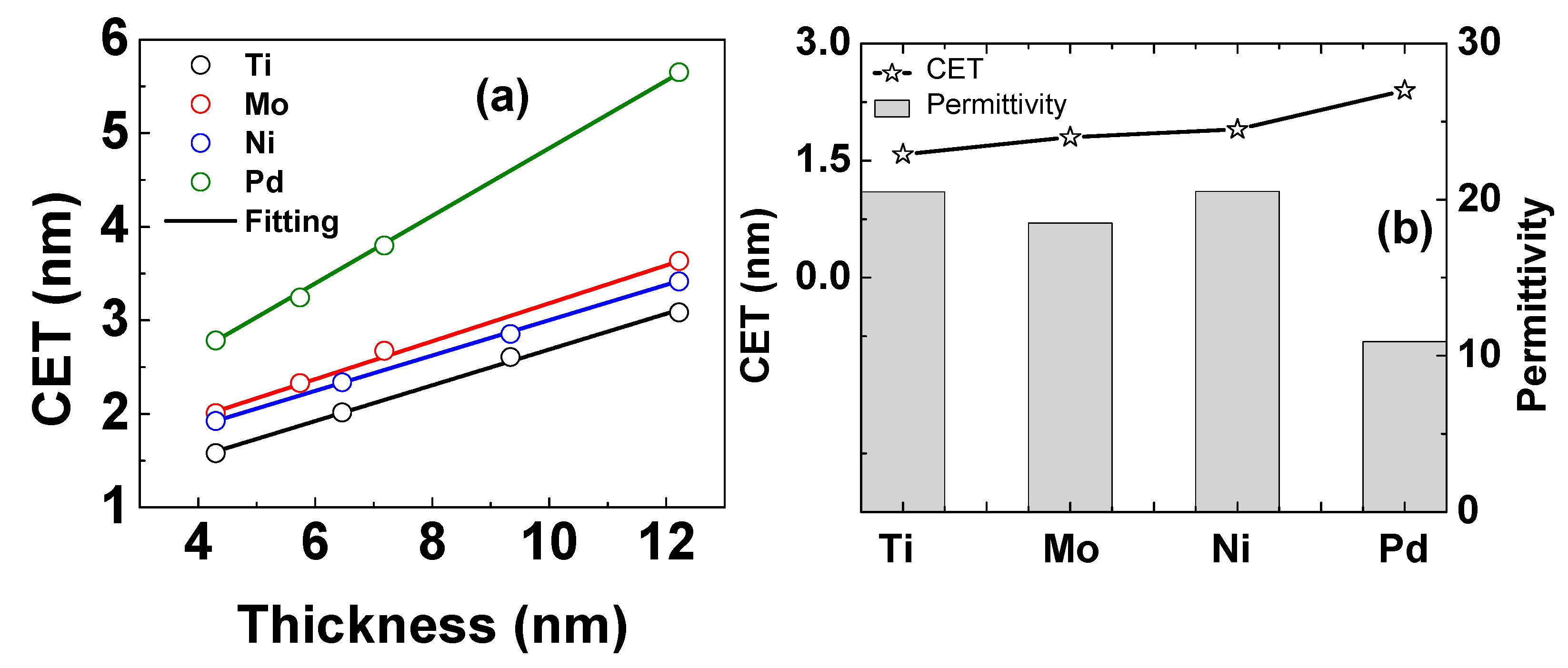
Figure 3a shows the capacitance oxide thickness (CET) at +2 V and 1 MHz versus the HfO2 thickness (tHfO2) curves of all samples. The total thickness of HfO2 and AlON in this study is large enough to neglect the quantum effect [41]. The charge centroid is expected to be at the AlON/InGaAs interface when identifying the thickness of the oxide in accumulation. CET is a function of the HfO2 thickness (tHfO2) following Equation (1).
where and tAlON are the permittivity of the HfO2 and the thickness of AlON, respectively, , ΨS and ΨS,G are the band bending at the channel and gate electrodes, respectively, and DS is the electric displacement in the substrate just beneath the oxide/InGaAs interface. Equation (1) allows the permittivity of the high-k layer to be extracted based on the slopes of the CET-tox curves in Figure 3a, without knowing the band bending at the channel and gate electrodes. The extracted values of permittivity are shown in Figure 3b. The values of permittivity of the Ti-, Mo-, and Ni-gated samples are the same, fluctuating around 18.5 to 21, which is in agreement with a previous report [42]. The permittivity of the Pd sample is ~11, too small to compare to others, which is likely due to the formation of a PdO layer [15] with a small permittivity of ~8 [43].
3.2. Effects of Gate Metals on Interface Traps and Border Traps
The impact of fast and slow traps on the electrical properties of HfO2 on IGA is examined via TCAD simulations using the parameters shown in Table 1. Interface and border traps are included at the AlON/IGA interface and within the band gap of HfO2 (for example, oxygen vacancies), respectively, to fit the simulation C-V curves to the ones observed in the experiment. The effects of the AlON/HfO2 interface traps on C-V curves are not separately investigated in this study because it is hard to distinguish this type of trap from others. Instead, this trap and border trap are considered as a single object. Additionally, a negative interface fixed charge of around 5.0 × 1011 cm−2 to 1.5 × 1012 cm−2, similar to that in a recent study, is included [44]. The interface fixed charges are related to the incorporation of nitrogen in high-k dielectrics during ALD deposition or in post-deposition treatment [45,46]. This charge is treated as a sheet of charge at the interface controlled by the interface boundary condition, which causes the shift of the C-V curves. On the other hand, interface traps and bulk traps are added as space charge directly into the right-hand side of Poisson’s equation:
where Ψ is the electrostatic potential, ε is the permittivity, ρ is the local space charge density, and are the ionized donor and acceptor impurity concentrations, respectively, and QT is the charge due to traps and defects. The total charge caused by the presence of traps in the right-hand side of Poisson’s equation can be defined by:
where and are the densities of the ionized donor-like and acceptor-like traps, respectively.
It is seen in Figure 4a–d that the simulation results fit well with the experiment. The process to calibrate the simulation curves consists of two steps: (i) adding interface traps to the AlON/IGA interface to fit C-V curves in the forward bias and (ii) simulating C-V curves in reverse bias to obtain hysteresis by adding border traps in the bandgap of HfO2. There are two types of interface traps: donor-like and acceptor-like. A donor-like trap can be either positive or neutral, and it is positively charged (ionized) as empty and neutral as filled (with an electron). An acceptor-like trap can be either negative or neutral, and it is neutral as empty and negatively charged (ionized) as filled (with an electron). One of the well-known methods to extract densities of interface traps (Dit) is the conductance method. This method is based on estimating the peak of equivalent parallel conductances calculated from measured impedance [47]. The advantage of this method is that the Dit can be extracted directly from experimental data. However, the extracted Dit is reported to be not correct in the case of large Dit, especially when Cox < qDit [47]. Another popular method is the Terman method. To extract Dit, the ideal C-V curve is plotted. The stretch-out of the experimental curve as compared to the ideal one provides the value of Dit. The Dit extracted by the Terman method is typically larger (~10 times) than that extracted by the conductance method [4].
Figure 4e shows the Dit of all samples extracted from TCAD simulations. It is seen that Dit is minimal at the mid gap, and acceptor-like densities are smaller as compared to donor-like densities for all samples. The lifetime of interface traps is extracted to be 2.9 × 10⁻⁹ s, which is the same as the previous study [48]. The smallest Dit (1.39 × 10¹¹ eV−1cm−2 acceptor-like traps, and 3.81 × 10¹¹ eV−1cm−2 donor-like traps) is in the sample with a Mo gate. This result is in accordance with the multi-frequency C-V curves in Figure 2b, where the Mo sample seems to not present any hump around 0 V at high frequency. In contrast, the highest Dit is in the Ti-gated sample, corresponding to the largest hump around 0 V at a high frequency, as shown in Figure 2a. The fact that the Dit from donor-like traps near the valence band edge of all samples is much smaller compared to those near the conduction band edge confirms the strong inversion of the multi-frequency C-V curves of all samples shown in Figure 2, implying freely moving minority carriers in the channel. In our previous report, a combination of Mo/Ti gate metal and the passivation layer AlN between Ti and HfO2 leads to a small Dit [4]. In that study, a thin AlN layer was believed to prevent the reaction between Ti and HfO2, diminishing the formation of oxygen vacancies in HfO2.
The extracted border traps are shown In Figure 4f. Because the border traps near the conduction band strongly affect the n-type substrate, only acceptor-like border traps are considered in this study [49]. To simulate the hysteresis of C-V curves, the Heiman method [50] is utilized. The traps are assumed to have a uniform distribution with depth in HfO2, but the capture cross-section and the lifetime of traps for electrons are a function of distance from the AlON/IGA interface:
where x is the distance from the interface to the trap position in HfO2, is the capture cross-section of traps for electrons at the interface, ns is the trap concentration at the interface, is the thermal velocity of electrons, and is determined from:
where EC, m*e, EtA, , and EtA are the conduction band minimum, the effective mass of the electron, the border trap level, the Planck constant, and the level of the acceptor-like trap, respectively. It is seen that the largest border traps of 2.2 × 10²⁰ eV−1cm−3 occur in the Pd sample, explaining the largest hysteresis of 0.76 V of CV curves in Figure 4c. The extracted lifetime of border traps at the interface is 2.5 × 10⁻⁵ s, which is larger than the interface traps. The value of lifetime is the same as in the study of Zhang et al. [51]. For the border traps in high-k, the values of lifetimes are calculated in Equation (5). Similar to the extracted Dit, the smallest value of border traps, an NBT of 4.46 × 10¹⁹ eV−1cm−3, also occurs in the Mo sample, which is confirmed by the smallest hysteresis in its C-V hysteresis of 0.11 V, as shown in Figure 4f. Although the work function of Ni and Pd is nearly the same, the quality of the Ni sample is much better than Pd. The reasons for the degradation have been discussed in our previous report, where the formation energy of the metal oxygen defect has a critical role that stabilizes the metal/high-k interface [15].
The effects of Dit and NBT are systematically studied in Figure 5. Figure 5a indicates that the ionization profiles of interface traps extracted from the TCAD simulation depend on the types of traps and their positions as compared to the charge neutrality level (CNL) at 0.21 eV inside the IGA band gap [52]. It is seen that donor-like traps are ionized above CNL, creating a positive charge at the interface. A complete ionization of the interface of donor-like traps generates a net positive charge, contributing to the total capacitance, which induces a negative shift and up-shift of C-V curves (pink solid line) compared to the ideal (black solid line) at a negative voltage, as shown in Figure 5b. Based on the stretch-out of C-V curves due to these shifts, it was reported that densities of interface traps could be extracted by the Terman method [47]. However, in our case, it was impossible to separate the densities of ionized and neutral traps using this method. Opposite to donor-like traps, acceptor-like traps are filled below the CNL, as shown in Figure 5a. These traps induce a net negative charge at the interface, the same as the interface-fixed charge, when they are completely ionized. These traps also cause a right shift of the C-V curve and a decrease in the accumulation capacitance, as shown in Figure 5b (pink solid line). To distinguish the effects of donor-like and acceptor-like traps on the charge density of the channel below HfO2, donor-like traps (Dit = 3.81 × 10¹¹ eV−1cm−2) or acceptor-like traps (Dit = 1.27 × 10¹¹ eV−1cm−2) are added at the mid gap of the Mo sample in our C-V simulation. It is clear that single donor-like traps shift the C-V curves up around 0 V (red dash line). This shift means that a hump around 0 V can be created when the Dit of donor-like traps is high and the measured frequency is small, as seen in the experiment in Figure 2a,c,d. The blue dashed line in Figure 5b illustrates that acceptor-like traps act as a sheet of a negative fixed charge and shift the C-V curves to positive voltage. The effect of the density of border traps on the C-V curves of the Mo sample is shown in Figure 5c. In all simulations, border traps are assumed to distribute in the dielectric with a maximum depth of 2 nm from the interface, and the continuously distributed states are represented by 20 discrete trap states along a depth of 2 nm, as shown in Figure 6a. It is seen that there is no C-V hysteresis when NBT = 4.47 × 10¹⁸ eV−1cm−3. The change in the order of NBT causes a significant variation of the hysteresis, and the hysteresis larger than 1.0 V is found as NBT = 4.47 × 1020 cm−3. The impact of a lifetime of border traps is considered in Figure 5d. Because only acceptor-like border traps near the conduction band edge are investigated, the lifetime affects meaningfully the accumulation region. Since the simulated frequency is 1 MHz, a lifetime of 2.9 × 10⁻³ s induces no consequence on C-V curves. The border traps have a substantial response if they have a lifetime smaller than 2.9 × 10⁻⁵ s, which is in agreement with the literature [51].
3.3. Properties of Metal/HfO2/AlON/In0.53Ga0.47As Structures
Band diagrams of all samples were extracted from the TCAD simulation at 0V, as shown in Figure 6a. The simulated band offsets of the HfO2/AlON/IGA structures were compared with data from XPS measurements, as shown in Figure 6b. The band offsets of the AlON/IGA and HfO2/AlON structures are extracted to be 2.47 eV and 0.35 eV, respectively, showing agreement between the experiment and simulation. Although five cycles of the AlN layer were deposited on IGA for passivation, XPS revealed that this layer was AlON [3]. It is found that low and high work function gate metals induce opposite bending in the band diagram. This bending depends on the flat band voltage described by [53]:
where VFB is the flat band voltage, ϕm is the work function of metals, ϕS is the semiconductor work function, Qf is the interface fixed charges, εSiO2 is the permittivity of SiO2, εox is the permittivity of HfO2, tox is its thickness, and ρox is bulk HfO2 charge density. The relationship between VFB and tox was reported to be linear in the HfO2/IGA moscap, so the effect of on VFB is much smaller compared to on VFB [3]. Because the density of interface fixed charge used to calibrate the C-V curves is quite similar ~1012 cm−2 in all samples, bending in the band diagram should be from the difference in metal work functions and the bulk charges shown in Figure 4f alone. Additionally, the border acceptor-like traps studied in this work are empty at 0 V, as shown in Figure 4f, referring to its neutral state at 0 V above the CNL. These trap charges also need a delay time to fill up. The opposite band bending (0.62 eV–0.89 eV) of the samples shown in Figure 6a is in agreement with the C-V curves in Figure 4a–d, illustrating a negative C-V shift of the Ti sample and a positive C-V shift of the others. This bend bending is also confirmed by the valence band maxima of XPS spectra measured at metal/HfO2 interfaces, as shown in Figure 6c.
To analyze the interaction of the metal/HfO2 interface, the factor that most impacts Dit and NBT is the convolution of the Hf 4f peaks shown in Figure 6d. All samples with a diameter of ~5 mm were mounted on an XPS holder using copper tape. The pressure of the XPS chamber is ~10−9 torr when the measurement was conducted. For the analysis, the core levels were determined by using XPSPEAK with a Gaussian–Lorentz line shape and Shirley background, with an uncertainty of the core position of 0.05 eV. Sample charging effects were corrected by placing the C 1s peak at a binding energy (BE) of 284.8 eV and shifting the rest of the regions accordingly. The binding energy, the spin–orbit splitting (SOS), and the full-width at half-maxima (FWHM) values used to fit the curves of the two samples are shown in Table 2. For the clean HfO2 sample, there are two peaks that are convoluted: an Hf 4f7/2 peak at 17.12 eV [3,54] and an In 4d peak at 18.47 eV [3,55], representing the In-O bond. The presence of an In peak with an area of ~10% is believed to be due to In diffusion from the InGaAs layer [55]. In the other samples, Hf 4f7/2 peaks were split into three peaks. One of them is the Hf 4f7/2, which appears in the clean HfO2 sample, denoted as a peak of deposited HfO2. The In-O peak in other samples was kept to have the same BE, SOS, FWHM, and area to ensure that it does not affect other peaks in the fitting process. It is seen that a new peak at 16.97 eV dominates in all samples (besides the peak of Hf 4f7/2), except in clean HfO2. The BE of this peak is in a range of the Hf 4f7/2 peak (from 14.3 eV for Hf metal to 18.3 eV for perfect HfO2 oxide) [56], so it can be inferred that gate metals react with the oxygen in HfO2, producing a complex interface that contains HfMO (M: Ti, Mo, Pd, and Ni). We denote Hf 4f7/2 in clean HfO2 and HfMO as Hf1 and Hf2 peaks, respectively. The area ratio of Hf2 and Hf1 peaks, AHf2/AHf1, should give us information relating to the oxidation of the gate metals because more oxidation causes a higher intensity of the Hf2 peak. The area ratios AHf2/AHf1 in the Ti, Mo, Pd, and Ni samples were extracted at 0.775, 0.296, 0.460, and 0.390, respectively, implying that the the Mo sample created the most stable interface on HfO2. Its XPS result is in agreement with its C-V behavior shown in Figure 2b, with the lowest values of Dit and NBT shown in Figure 4e,f. The stability of the Mo/HfO2 and Ni/HfO2 interfaces is also confirmed in the TEM measurement shown in Figure S2b,d (supporting information). Oppositely, the Ti/HfO2 interface has the highest ratio, AHf2/AHf1, indicating a strong reaction between Ti and O2− in HfO2. This reaction is observed in Figure S2a (supporting information), showing the increase in roughness at the Ti/HfO2 interface. This reaction can be suppressed by passivating the HfO2 surface using an ultra-thin AlN layer, which was reported in our previous work [4]. The area ratio AHf2/AHf1 in the Pd sample is slightly higher than the Ni sample, indicating that Pd-O facilitates oxidation at the AlON/IGA interface due to the transportation of oxygen vacancies in HfO2. Yoshida et al. reported that Pd-O induced a thin In-O layer between HfO2 and IGA [57]. The effect of Pd-O on the HfO2 layer should be similar to this study. However, the TEM image in Figure S2c does not show the In-O layer. Instead, Pd-O causes the defects in the AlON layer, illustrated by the white arrows in Figure S2c, supporting information. The difference in the formation of the In-O layer at the high-k/IGA interface is due to the fact that AlON is an excellent passivation layer [1]. The results indicate that the reaction at the metal/HfO2 interface is the main factor that creates an oxygen vacancy in HfO2, contributing to high Dit at the HfO2/IGA interface and high NBT in bulk HfO2. The high value of NBT is a disadvantage in devices for logic applications but an advantage in memory devices.
Figure 7 shows the leakage current through HfO2. These currents can be described by the tunneling effects in the Fowler–Nordheim regime [58]:
where and represent the tunneling barrier and oxide electric field, respectively. It is clear that the Ti sample has high leakage current shown in Figure 7a due to the lower barrier of the AlON layer shown in Figure 6a and the high value of high Dit and NBT shown in Figure 4e,f. Oppositely, the Mo and Ni samples have the lowest leakage current. These two samples have the same band bending shown in Figure 7a and the low Dit and NBT shown in Figure 4e,f. For logic applications, Dit can be benchmarked as a function of CET, as shown in Figure 7b. Our extracted value is revealed to be the smallest (1 × 10¹¹ eV−1cm−2 for acceptor-like traps) compared to other reports.
4. Conclusions
In summary, the impact of gate metals on interface traps and border traps in the metal/HfO2/AlN/InGaAs structure was systematically studied. Due to oxidation at the metal/HfO2 interface, low work function metal Ti creates the highest NBT in HfO2, while the middle work function metal Mo induces the lowest Dit and NBT. The TCAD simulations confirm the occupation of traps around the CNL, where donor-like traps are ionized above CNL and acceptor-like traps are ionized below this level. The extracted lifetime of interface and border traps in this study are 2.9 × 10⁻⁹ s and 2.9 × 10⁻⁵ s, respectively. Interface traps distort the C-V characteristics, whereas border traps cause their hysteresis. The Heiman method was utilized to investigate the border traps in HfO2. The lowest Dit and NBT were found to be 1.39 × 10¹¹ eV−1cm−2 and 4.46 × 10¹⁹ eV−1cm−3, respectively, for middle work function metal Mo due to a stable interface observed in XPS as well as a flat band voltage of 0 V. The results of this study provide guidance in the choice of gate metal for microelectronic devices and random-access memory.
Supplementary Materials
The following supporting information can be downloaded at https://www.mdpi.com/article/10.3390/mi14081606/s1, Figure S1: flow chart of process simulation in Silvaco TCAD to study the effects of interface and border traps in metal/HfO2/AlON/IGA structures.; Figure S2: TEM cross sections of metal/HfO2/AlON/IGA structures. Metal: (a) Ti, (b) Mo, (c) Pd, (d) Ni. The Mo/HfO2 and Ni/HfO2 interfaces were found to have no interdiffusion, while the oxidation was observed at Ti/HfO2 interface for Ti sample (indicated by white arrows). White arrows in Figure S2(c) demonstrate that Pd gate metal induces many defects in AlON passivation layer.
Author Contributions
Investigation, H.-B.D., Q.-H.L., P.V.P., A.-V.P.-G., T.-S.N., H.-M.L. and M.M.D.S.; formal analysis, H.-B.D.; conceptualization, H.-B.D.; writing—review and editing, H.-B.D., Q.-H.L., P.V.P., A.-V.P.-G., T.-S.N., H.-M.L. and M.M.D.S.; funding acquisition, H.-B.D.; supervision, H.-B.D. All authors have read and agreed to the published version of the manuscript.
Funding
This work was funded by the Ho Chi Minh City University of Technology and Education, Vietnam (grant No. T2022-29).
Institutional Review Board Statement
Not applicable
Informed Consent Statement
Not applicable
Data Availability Statement
The data that support the findings of this study are available from the corresponding author upon reasonable request.
Conflicts of Interest
The authors declare no conflict of interest.
References
- Luc, Q.H.; Do, H.B.; Ha, M.T.H.; Hu, C.C.; Lin, Y.C.; Chang, E.Y. Plasma Enhanced Atomic Layer Deposition Passivated HfO2/AlN/In0.53Ga0.47As MOSCAPs with Sub-Nanometer Equivalent Oxide Thickness and Low Interface Trap Density. IEEE Electron Device Lett. 2015, 36, 1277–1280. [Google Scholar] [CrossRef]
- Luc, Q.H.; Cheng, S.P.; Chang, P.C.; Do, H.B.; Chen, J.H.; Ha, M.T.H.; Huynh, S.H.; Hu, C.C.; Lin, Y.C.; Chang, E.Y. Effects of In-Situ Plasma-Enhanced Atomic Layer Deposition Treatment on the Performance of HfO2/In0.53Ga0.47As Metal–Oxide–Semiconductor Field-Effect Transistors. IEEE Electron Device Lett. 2016, 37, 974–977. [Google Scholar] [CrossRef]
- Do, H.B.; Luc, Q.H.; Ha, M.T.H.; Hu, C.C.; Lin, Y.C.; Chang, E.Y. Impact of AlN Interfacial Dipole on Effective Work Function of Ni and Band Alignment of Ni/HfO2/In0.53Ga0.47As Gate-Stack. IEEE Trans. Electron Devices 2015, 62, 3987–3991. [Google Scholar] [CrossRef]
- Do, H.B.; Luc, Q.H.; Ha, M.T.H.; Huynh, S.H.; Nguyen, T.A.; Hu, C.; Lin, Y.C.; Chang, E.Y. Investigation of Mo/Ti/AlN/HfO2 High-k Metal Gate Stack for Low Power Consumption InGaAs NMOS Device Application. IEEE Electron Device Lett. 2017, 38, 552–555. [Google Scholar] [CrossRef]
- Luc, Q.H.; Fan-Chiang, C.C.; Huynh, S.H.; Huang, P.; Do, H.B.; Ha, M.T.H.; Jin, Y.D.; Nguyen, T.A.; Zhang, K.Y.; Wang, H.C.; et al. First Experimental Demonstration of Negative Capacitance InGaAs MOSFETs with Hf0.5Zr0.5O2 Ferroelectric Gate Stack. In Proceedings of the 2018 IEEE Symposium on VLSI Technology, Honolulu, HI, USA, 18–22 June 2018. [Google Scholar]
- Song, T.; Tan, H.; Estandía, S.; Gàzquez, J.; Gich, M.; Dix, N.; Fina, I.; Sánchez, F. Improved polarization and endurance in ferroelectric Hf0.5Zr0.5O2 films on SrTiO3. Nanoscale 2022, 14, 2337–2343. [Google Scholar] [CrossRef]
- Wan, J.; Chen, X.; Ji, L.; Tu, Z.; Wu, H.; Liu, C. Ferroelectricity of Hf0.5Zr0.5O2 Thin Films Free from the Influence of Electrodes by Using Al2O3 Capping Layers. IEEE Trans. Electron Devices 2022, 69, 1805–1810. [Google Scholar] [CrossRef]
- Wang, H.; Liu, J.; Wei, J.; Xiao, K.; Chen, Y.; Jiang, Y.-L.; Wan, J. Au Nanoparticles/HfO2/Fully Depleted Silicon-on-Insulator MOSFET Enabled Rapid Detection of Zeptomole COVID-19 Gene with Electrostatic Enrichment Process. IEEE Trans. Electron Devices 2023, 70, 1236–1242. [Google Scholar] [CrossRef] [PubMed]
- Das, S.K.; Chettri, B.; Karki, P.; Chettri, P.; Deka, U.; Sharma, B. Analysis of certain electrical properties in Silicon nanowire field-effect transistors with high-κ HfO2 as gate dielectrics. In Proceedings of the 2022 IEEE International Conference of Electron Devices Society Kolkata Chapter (EDKCON), Kolkata, India, 26–27 November 2022. [Google Scholar]
- Ram, M.S.; Svensson, J.; Skog, S.; Johannesson, S.; Wernersson, L.-E. Low-Frequency Noise in Vertical InAs/InGaAs Gate-All-Around MOSFETs at 15 K for Cryogenic Applications. IEEE Electron Device Lett. 2022, 43, 2033–2036. [Google Scholar] [CrossRef]
- Liu, C.; Wang, Z.; Zhang, Y.; Lü, H.; Zhang, Y.M. Nanolaminated HfO2/Al2O3 Dielectrics for High-Performance Silicon Nanomembrane Based Field-Effect Transistors on Biodegradable Substrates. Adv. Mater. Interfaces 2022, 9, 2201477. [Google Scholar]
- Kumar, P.; Koley, K.; Goswami, R.; Maurya, A.; Kumar, S. Electrical Noise Behaviour of High-k Gate-All-Around MOSFET Based on Two-Port Device Network Analysis. In Proceedings of the 2022 14th International Conference on Information Technology and Electrical Engineering (ICITEE), Changsha, China, 4–6 November 2022. [Google Scholar]
- Kumar, P.; Vashishath, M.; Gupta, N.; Gupta, R. High-k Dielectric Double Gate Junctionless (DG-JL) MOSFET for Ultra Low Power Applications- Analytical Model. Silicon 2022, 14, 7725–7734. [Google Scholar] [CrossRef]
- Takagi, K.; Ono, T. First-principles study on leakage current caused by oxygen vacancies at HfO2/SiO2/Si interface. Jpn. J. Appl. Phys. 2018, 57, 066501. [Google Scholar] [CrossRef]
- Do, H.B.; Luc, Q.H.; Ha, M.T.H.; Huynh, S.H.; Nguyen, T.A.; Lin, Y.C.; Chang, E.Y. Study of the interface stability of the metal (Mo, Ni, Pd)/HfO2/AlN/InGaAs MOS devices. AIP Adv. 2017, 7, 085208. [Google Scholar] [CrossRef]
- Zaffora, A.; Macaluso, R.; Habazaki, H.; Valov, I.; Santamaria, M. Electrochemically prepared oxides for resistive switching devices. Electrochim. Acta 2018, 274, 103–111. [Google Scholar] [CrossRef]
- Kim, S.J.; Mohan, J.; Summerfelt, S.R.; Kim, J. Ferroelectric Hf0.5Zr0.5O2 Thin Films: A Review of Recent Advances. JOM 2019, 71, 246–255. [Google Scholar] [CrossRef]
- Chen, Y.Y.; Goux, L.; Clima, S.; Govoreanu, B.; Degraeve, R.; Kar, G.S.; Fantini, A.; Groeseneken, G.; Wouters, D.J.; Jurczak, M. Endurance/Retention Trade-off on HfO2/Metal Cap 1T1R Bipolar RRAM. IEEE Trans. Electron Devices 2013, 60, 1114–1121. [Google Scholar] [CrossRef]
- Dirkmann, S.; Kaiser, J.; Wenger, C.; Mussenbrock, T. Filament Growth and Resistive Switching in Hafnium Oxide Memristive Devices. ACS Appl. Mater. Interfaces 2018, 10, 14857–14868. [Google Scholar] [CrossRef]
- Petzold, S.; Miranda, E.; Sharath, S.U.; Muñoz-Gorriz, J.; Vogel, T.; Piros, E.; Kaiser, N.; Eilhardt, R.; Zintler, A.; Molina-Luna, L.; et al. Analysis and simulation of the multiple resistive switching modes occurring in HfOx-based resistive random access memories using memdiodes. J. Appl. Phys. 2019, 125, 234503. [Google Scholar] [CrossRef] [Green Version]
- Cheynet, M.C.; Pokrant, S.; Tichelaar, F.D.; Rouvière, J.-L. Crystal structure and band gap determination of HfO2 thin films. J. Appl. Phys. 2007, 101, 054101. [Google Scholar] [CrossRef] [Green Version]
- Rushchanskii, K.Z.; Blügel, S.; Ležaić, M. Routes for increasing endurance and retention in HfO2-based resistive switching memories. Phys. Rev. Mater. 2018, 2, 115002. [Google Scholar] [CrossRef] [Green Version]
- Xue, K.H.; Blaise, P.; Fonseca, L.R.; Nishi, Y. Prediction of Semimetallic Tetragonal Hf2O3 and Zr2O3 from First Principles. Phys. Rev. Lett. 2013, 110, 065502. [Google Scholar] [CrossRef] [PubMed] [Green Version]
- Rushchanskii, K.Z.; Blügel, S.; Ležaić, M. Ab initio phase diagrams of Hf–O, Zr–O and Y–O: A comparative study. Faraday Discuss. 2019, 213, 321–337. [Google Scholar] [CrossRef] [PubMed]
- Vais, A.; Alian, A.; Nyns, L.; Franco, J.; Sioncke, S.; Putcha, V.; Yu, H.; Mols, Y.; Rooyackers, R.; Lin, D.; et al. Record mobility (μeff ~3100 cm2/V-s) and reliability performance (Vov ~0.5 V for 10 yr operation) of In0.53Ga0.47As MOS devices using improved surface preparation and a novel interfacial layer. In Proceedings of the 2016 IEEE Symposium on VLSI Technology, Honolulu, HI, USA, 14–16 June 2016. [Google Scholar]
- Lin, J.; Zhao, X.; Clavero, I.M.; Antoniadis, D.A.; del Alamo, J.A. A Scaling Study of Excess off-State Current in InGaAs Quantum-Well MOSFETs. IEEE Trans. Electron Devices 2019, 66, 1208–1212. [Google Scholar] [CrossRef]
- Cai, X.; Vardi, A.; Grajal, J.; del Alamo, J.A. Reassessing InGaAs for Logic: Mobility Extraction in sub-10 nm Fin-Width FinFETs. In Proceedings of the 2019 Symposium on VLSI Technology, Kyoto, Japan, 9–14 June 2019. [Google Scholar]
- Ko, H.-L.; Luc, Q.H.; Huang, P.; Wu, J.-Y.; Chen, S.-M.; Tran, N.-A.; Hsu, H.-T.; Chang, E.Y. Sub-10 nm Top Width Nanowire InGaAs Gate-All-Around MOSFETs with Improved Subthreshold Characteristics and Device Reliability. IEEE J. Electron Devices Soc. 2022, 10, 188–191. [Google Scholar] [CrossRef]
- Cai, X.; Vardi, A.; Grajal, J.; del Alamo, J.A. A New Technique for Mobility Extraction in MOSFETs in the Presence of Prominent Gate Oxide Trapping: Application to InGaAs MOSFETs. IEEE Trans. Electron Devices 2020, 67, 3075–3081. [Google Scholar] [CrossRef]
- Pallecchi, I.; Grassano, G.; Marré, D.; Pellegrino, L.; Putti, M.; Siri, A.S. SrTiO3-based metal–insulator–semiconductor heterostructures. Appl. Phys. Lett. 2001, 78, 2244–2246. [Google Scholar] [CrossRef]
- Xuan, Y.; Wu, Y.Q.; Shen, T.; Yang, T.; Ye, P.D. High performance submicron inversion-type enhancement-mode InGaAs MOSFETs with ALD Al2O3, HfO2 and HfAlO as gate dielectrics. In Proceedings of the 2007 IEEE International Electron Devices Meeting, Washington, DC, USA, 10–12 December 2007. [Google Scholar]
- Putcha, V.; Franco, J.; Vais, A.; Kaczer, B.; Xie, Q.; Maes, J.W.; Tang, F.; Givens, M.; Collaert, N.; Linten, D.; et al. Extensive assessment of the charge-trapping kinetics in InGaAs MOS gate-stacks for the demonstration of improved BTI reliability. Microelectron. Reliab. 2020, 115, 113996. [Google Scholar] [CrossRef]
- Li, Y.; Deng, S.; Li, J.; Li, G.; Zhang, S.; Jin, Y. Investigation on HfO2 properties grown by ALD using TDMAH as precursor. Vacuum 2022, 203, 111243. [Google Scholar] [CrossRef]
- Robertson, J. High dielectric constant oxides. Eur. Phys. J. Appl. Phys. 2004, 28, 265–291. [Google Scholar] [CrossRef] [Green Version]
- Yeo, Y.-C.; King, T.-J.; Hu, C. Direct tunneling leakage current and scalability of alternative gate dielectrics. Appl. Phys. Lett. 2002, 81, 2091–2093. [Google Scholar] [CrossRef]
- Michaelson, H.B. The work function of the elements and its periodicity. J. Appl. Phys. 2008, 48, 4729–4733. [Google Scholar] [CrossRef]
- Stemmer, S.; Chobpattana, V.; Rajan, S. Frequency dispersion in III–V metal-oxide-semiconductor capacitors. Appl. Phys. Lett. 2012, 100, 233510. [Google Scholar] [CrossRef] [Green Version]
- Ji, Z.; Zhang, X.; Franco, J.; Gao, R.; Duan, M.; Zhang, J.F.; Zhang, W.D.; Kaczer, B.; Alian, A.; Linten, D.; et al. An Investigation on Border Traps in III–V MOSFETs with an In0.53Ga0.47As Channel. IEEE Trans. Electron Devices 2015, 62, 3633–3639. [Google Scholar] [CrossRef]
- Sicre, S.B.F.; Souza, M.M.D. Analysis of Pb Centers in Ultrathin Hafnium Silicate Gate Stacks. IEEE Trans. Electron Devices 2007, 54, 2551–2555. [Google Scholar] [CrossRef]
- Chang, Y.C.; Huang, M.L.; Lee, K.Y.; Lee, Y.J.; Lin, T.D.; Hong, M.; Kwo, J.; Lay, T.S.; Liao, C.C.; Cheng, K.Y. Atomic-layer-deposited HfO2 on In0.53Ga0.47As: Passivation and energy-band parameters. Appl. Phys. Lett. 2008, 92, 072901. [Google Scholar] [CrossRef] [Green Version]
- Sune, J.; Olivo, P.; Ricco, B. Quantum-mechanical modeling of accumulation layers in MOS structure. IEEE Trans. Electron Devices 1992, 39, 1732–1739. [Google Scholar] [CrossRef]
- Park, P.K.; Kang, S.-W. Enhancement of dielectric constant in HfO2 thin films by the addition of Al2O3. Appl. Phys. Lett. 2006, 89, 192905. [Google Scholar] [CrossRef] [Green Version]
- Madelung, O.; Rössler, U.; Schulz, M. (Eds.) PdO: Optical properties, dielectric constant: Datasheet from Landolt-Börnstein—Group III Condensed Matter. In Non-Tetrahedrally Bonded Binary Compounds II; SpringerMaterials; Springer: Berlin/Heidelberg, Germany, 2000; Volume 41D. [Google Scholar] [CrossRef]
- Kim, H.; Chavan, V.D.; Aziz, J.; Ko, B.; Lee, J.-S.; Rho, J.; Dongale, T.D.; Choi, K.-K.; Kim, D.-K. Effect of ALD Processes on Physical and Electrical Properties of HfO2 Dielectrics for the Surface Passivation of a CMOS Image Sensor Application. IEEE Access 2022, 10, 68724–68730. [Google Scholar] [CrossRef]
- Palumbo, F.; Krylov, I.; Eizenberg, M. Comparison of the degradation characteristics of AlON/InGaAs and Al2O3/InGaAs stacks. J. Appl. Phys. 2015, 117, 104103. [Google Scholar] [CrossRef] [Green Version]
- Choi, M.; Lyons, J.L.; Janotti, A.; Van de Walle, C.G. Impact of carbon and nitrogen impurities in high-κ dielectrics on metal-oxide-semiconductor devices. Appl. Phys. Lett. 2013, 102, 142902. [Google Scholar] [CrossRef] [Green Version]
- Engel-Herbert, R.; Hwang, Y.; Stemmer, S. Comparison of methods to quantify interface trap densities at dielectric/III–V semiconductor interfaces. J. Appl. Phys. 2010, 108, 124101. [Google Scholar] [CrossRef] [Green Version]
- Ahrenkiel, R.K.; Ellingson, R.; Johnston, S.; Wanlass, M. Recombination lifetime of In0.53Ga0.47As as a function of doping density. Appl. Phys. Lett. 1998, 72, 3470–3472. [Google Scholar] [CrossRef] [Green Version]
- Roll, G.; Mo, J.; Lind, E.; Johansson, S.; Wernersson, L.-E. Defect evaluation in InGaAs field effect transistors with HfO2 or Al2O3 dielectric. Appl. Phys. Lett. 2015, 106, 203503. [Google Scholar] [CrossRef]
- Heiman, F.P.; Warfield, G. The effects of oxide traps on the MOS capacitance. IEEE Trans. Electron Devices 1965, 12, 167–178. [Google Scholar] [CrossRef] [Green Version]
- Zhang, X.-Y.; Hsu, C.-H.; Cho, Y.-S.; Lien, S.-Y.; Zhu, W.-Z.; Chen, S.-Y.; Huang, W.; Xie, L.-G.; Chen, L.-D.; Zou, X.-Y.; et al. Simulation and Fabrication of HfO2 Thin Films Passivating Si from a Numerical Computer and Remote Plasma ALD. Appl. Sci. 2017, 7, 1244. [Google Scholar] [CrossRef] [Green Version]
- Xia, H.; Li, T.-X.; Tang, H.-J.; Zhu, L.; Li, X.; Gong, H.-M.; Lu, W. Nanoscale imaging of the photoresponse in PN junctions of InGaAs infrared detector. Sci. Rep. 2016, 6, 21544. [Google Scholar] [CrossRef] [PubMed] [Green Version]
- Winter, R.; Krylov, I.; Ahn, J.; McIntyre, P.C.; Eizenberg, M. The effect of post oxide deposition annealing on the effective work function in metal/Al2O3/InGaAs gate stack. Appl. Phys. Lett. 2014, 104, 202103. [Google Scholar] [CrossRef]
- Das, T.; Mahata, C.; Maiti, C.K.; Miranda, E.; Sutradhar, G.; Bose, P.K. Effects of Ti incorporation on the interface properties and band alignment of HfTaOx thin films on sulfur passivated GaAs. Appl. Phys. Lett. 2011, 98, 022901. [Google Scholar] [CrossRef]
- Sanchez-Martinez, A.; Ceballos-Sanchez, O.; Vazquez-Lepe, M.O.; Duong, T.; Arroyave, R.; Espinosa-Magaña, F.; Herrera-Gomez, A. Diffusion of In and Ga in TiN/HfO2/InGaAs nanofilms. J. Appl. Phys. 2013, 114, 143504. [Google Scholar] [CrossRef]
- Application Note. Characterization of High-k Dielectric Materials on Silicon Using Angle Resolved XPS; Thermo Fisher Scientific Inc.: Bartlesville, OK, USA, 2008. [Google Scholar]
- Yoshida, S.; Lin, D.; Vais, A.; Alian, A.; Franco, J.; El Kazzi, S.; Mols, Y.; Miyanami, Y.; Nakazawa, M.; Collaert, N.; et al. Systematic study of interfacial reactions induced by metal electrodes in high-k/InGaAs gate stacks. Appl. Phys. Lett. 2016, 109, 172101. [Google Scholar] [CrossRef]
- Olivo, P.; Sune, J.; Ricco, B. Determination of the Si-SiO2/barrier height from the Fowler-Nordheim plot. IEEE Electron Device Lett. 1991, 12, 620–622. [Google Scholar] [CrossRef]
- Suzuki, R.; Taoka, N.; Yokoyama, M.; Lee, S.; Kim, S.H.; Hoshii, T.; Yasuda, T.; Jevasuwan, W.; Maeda, T.; Ichikawa, O.; et al. 1-nm-capacitance-equivalent-thickness HfO2/Al2O3/InGaAs metal-oxide-semiconductor structure with low interface trap density and low gate leakage current density. Appl. Phys. Lett. 2012, 100, 132906. [Google Scholar] [CrossRef]
- Eom, S.-K.; Kong, M.-W.; Kang, M.-J.; Lee, J.-G.; Cha, H.-Y.; Seo, K.-S. Enhanced Interface Characteristics of PA-ALD HfOxNy/InGaAs MOSCAPs Using IPA Oxygen Reactant and Cyclic N2 Plasma. IEEE Electron Device Lett. 2018, 39, 1636–1639. [Google Scholar] [CrossRef]
Figure 1.
(a) Process of fabrication of HfO2/In0.53Ga0.47As MOSCAPs. (b) The schematic cross-section and HRTEM image of the metal/HfO2/In0.53Ga0.47As structure after PDA. (c) The relationship between HfO2 thickness and the number of cycles in the ALD chamber. The growth rate was determined at ~0.73 Å/cycle.

Figure 2.
Multi-frequency (1 kHz–1 MHz) C-V characteristics of MOSCAPs with different gate metals: (a) Ti, (b) Mo, (c) Pd, and (d) Ni. A hump around 0 V and high C-V dispersion is found in the Ti sample, indicating the presence of high densities of interface (Dit) and border traps (NBT). Oppositely, the lowest capacitance is in the Pd sample, referring to the degradation of permittivity of HfO2 when Pd is used as a gate metal. The best C-V behavior without hump around 0 V and small C-V dispersion is in the Mo sample (highlighted by blue circles), implying the lowest Dit and NBT.

Figure 3.
(a) Equivalent capacitance thickness (CET) versus physical oxide thickness of all samples. (b) Equivalent capacitance thickness (CET) and permittivity of all samples for a physical oxide thickness of 4.3 nm.
Figure 3.
(a) Equivalent capacitance thickness (CET) versus physical oxide thickness of all samples. (b) Equivalent capacitance thickness (CET) and permittivity of all samples for a physical oxide thickness of 4.3 nm.

Figure 4.
Results of C-V characteristics at 1 MHz from TCAD simulations and experiment of (a) Ti, (b) Mo (c) Pd, and (d) Ni samples. The up and down arrows illustrate the forward and reverse sweep of C-V curves, respectively. (e) Densities of interface traps extracted from TCAD simulations of the C-V curves in (a–d). (f) The densities of border traps and the difference in flat band voltage of the samples are shown in (a–d).

Figure 5.
(a) The distribution of ionized donor-like and acceptor-like traps at the AlON/InGaAs interface. Trap positions are compared with the conduction band minimum of InGaAs. (b) Effects of the kinds of interface traps on the C-V behaviors. Impacts of (c) densities and (d) lifetime of border traps on the C-V behaviors. The black arrows highlight the shift of C-V curves under the effects of interface traps, border traps, and the lifetime of traps.

Figure 6.
(a) Band diagram of a metal/HfO2/AlON/InGaAs structure extracted by TCAD simulation. (b) Valence band maxima of an HfO2/AlON/IGA structure derived from XPS measurement. (c) Valence band maxima of metal/HfO2 structures derived from XPS measurement. (d) Hf 4f7/2 of clean HfO2 surface and (Ti, Mo, Pd, Ni)/HfO2 interfaces.

Figure 7.
(a) I-V characteristics of M/HfO2 MOSCAPS, M = Ti, Mo, Pd, Ni. (b) Benchmark of Dit as a function of CET of Mo/HfO2/IGA MOSCAPs [2,59,60].


Table 1.
Parameters used in HfO2/IGA MOSCAPs.
| Material Parameters | HfO2 | AlON | In0.53Ga0.47As 1 |
|---|---|---|---|
| Band gap (eV) | 5.7 [34] | 7 [34] | 0.734 |
| Electron affinity (eV) | 2.52 2 | 0.882 | 4.67 |
| Permittivity | 10.9–21 3 | 8.8 [34] | 13.9 |
| Effective density of state in the conduction band (cm−3) | - | - | 2.1 × 10¹⁷ |
| Effective density of state in the valence band (cm−3) | - | - | 7.7 × 10¹⁸ |
| Intrinsic carrier concentration (cm−3) | - | - | 8.72 × 10¹¹ |
| Electron mobility (cm2/V·s) | - | - | 104 |
| Effective electron mass | - | - | 0.041 mo |
| Effective hole mass | 0.46 mo | ||
| Tunnelling effective masses | 0.17 mo [35] | 0.35 mo [35] | - |
| Saturated electron drift velocity (cm/s) | - | - | 2.5 × 10⁷ |
| Saturated hole drift velocity (cm/s) | - | - | 7.7 × 10⁶ |
1 Parameters of InGaAs are default values from TCAD. 2 Based on the band offset of HfO2/InGaAs, extracted from XPS spectra. 3 Values extracted from CET thickness curves.
Table 2.
BE, SOS, and equal FWHM values were applied to fit the curves in Figure 6d (eV).
Table 2.
BE, SOS, and equal FWHM values were applied to fit the curves in Figure 6d (eV).
| Hf 4f7/2 (Clean HfO2) | In-O | Hf 4f7/2 (HfMO), M = Ti, Mo, Pd, Ni | |
|---|---|---|---|
| BE (eV) | 17.12 | 18.47 | 16.97 |
| SOS (eV) | 1.68 | 0.8 | 1.68 |
| FWHM | 1.62 | 1.28 | 1.68 |
Disclaimer/Publisher’s Note: The statements, opinions and data contained in all publications are solely those of the individual author(s) and contributor(s) and not of MDPI and/or the editor(s). MDPI and/or the editor(s) disclaim responsibility for any injury to people or property resulting from any ideas, methods, instructions or products referred to in the content. |
© 2023 by the authors. Licensee MDPI, Basel, Switzerland. This article is an open access article distributed under the terms and conditions of the Creative Commons Attribution (CC BY) license (https://creativecommons.org/licenses/by/4.0/).
Share and Cite
MDPI and ACS Style
Do, H.-B.; Luc, Q.-H.; Pham, P.V.; Phan-Gia, A.-V.; Nguyen, T.-S.; Le, H.-M.; De Souza, M.M. Metal-Induced Trap States: The Roles of Interface and Border Traps in HfO2/InGaAs. Micromachines 2023, 14, 1606. https://doi.org/10.3390/mi14081606
AMA Style
Do H-B, Luc Q-H, Pham PV, Phan-Gia A-V, Nguyen T-S, Le H-M, De Souza MM. Metal-Induced Trap States: The Roles of Interface and Border Traps in HfO2/InGaAs. Micromachines. 2023; 14(8):1606. https://doi.org/10.3390/mi14081606
Chicago/Turabian StyleDo, Huy-Binh, Quang-Ho Luc, Phuong V. Pham, Anh-Vu Phan-Gia, Thanh-Son Nguyen, Hoang-Minh Le, and Maria Merlyne De Souza. 2023. "Metal-Induced Trap States: The Roles of Interface and Border Traps in HfO2/InGaAs" Micromachines 14, no. 8: 1606. https://doi.org/10.3390/mi14081606
Note that from the first issue of 2016, this journal uses article numbers instead of page numbers. See further details here.