Al-Si10-Mg Manufactured by Selective Laser Melting: Microstructure Sensitivity to Close Values of the Heat Input


1
Department of Engineering for Innovation, University of Salento, Via per Monteroni, 73100 Lecce, Italy
2
ENEA, Division for Sustainable Materials, Research Centre of Brindisi, S.S.7 Appia Km 706, 72100 Brindisi, Italy
*
Author to whom correspondence should be addressed.
Metals 2023, 13(3), 590; https://doi.org/10.3390/met13030590
Submission received: 16 February 2023
/
Revised: 7 March 2023
/
Accepted: 8 March 2023
/
Published: 14 March 2023
(This article belongs to the Section Additive Manufacturing)
Abstract
:Selective Laser Melting (SLM) is an attractive Additive Manufacturing (AM) technology for the fabrication of metallic components with complex structures and high performances. This process fulfills the goals of sustainable production by reducing material waste, optimizing product topology, and recycling metallic powder. Aluminum alloys exhibit also sustainable performances being lightweight and recyclable. Al-Si10-Mg alloy is suitable for SLM processing due to its good castability, good strength, wear, and corrosion resistance. However, the laser processing of aluminum alloys to date needs to be optimized. In this study, the authors have analyzed the role of close values of heat input on microstructure and defects (Electron and Optical microscope, DRX analysis), porosity (optical microscope and X-ray tomography), melting pool geometries (both in transversal and longitudinal sections of the samples) and mechanical performance (hardness and tensile test) of Al-Si10-Mg samples. The results have shown that even at very close values of energy density, the microstructure and properties of the samples differ from each other.
1. Introduction
Aluminum alloys are employed in many industries, such as automotive, aerospace, food, biomedical, construction, and electronic field because they are lightweight with good specific strength, easy processability, good corrosion resistance, and excellent electrical and thermal conductivity [1,2,3,4].
The most important group of aluminum alloys for casting purposes is based on the Al-Si system, particularly on the hypoeutectic composition (less than 11.7% in weight of silicon), and constitutes 85–90% of the total aluminum alloys for casting [1,2]. In fact, those alloys assure good castability and high fluidity due to Si eutectic and low solidification shrinkage. As the content of Si increases toward the eutectic point, both the melting point and solidification temperature range are reduced. So, in the near eutectic aluminum alloys, the castability is improved and shrinkage porosity is reduced. Moreover, with the addition of Mg, the Al-Si alloys become heat treatable by aging treatment and so acquire higher specific strength by precipitation of β’ (Mg2Si) particles [1,2]. The Al-Si10-Mg alloy, containing Mg additions equal to 0.20–0.40 (weight%) is therefore widely employed in those industrial fields, such as the automotive and aerospace ones, where lightweight and high specific resistance are essential requirements [4].
Anyway, despite the good properties of Al-Si10-Mg alloy, the traditional casting processes usually can induce in the components a coarse microstructure and element segregation due to a low solidification rate that lowers the mechanical properties of the parts.
Selective Laser Melting (SLM) is an attractive technology for the fabrication of metallic components with high performance. SLM utilizes a high-energy laser beam to completely melt metal powder in a protective atmosphere along the laser path, and this molten metal rapidly solidifies [4,5,6]. By repeating this step and overlapping layer by layer, a three-dimensional component is formed in a one-step process with considerable geometrical freedom. The cooling rate of the melting pool is very high and increases with the laser speed, which usually ranges from 100–1000 mm/s [4]. Such a rapid cooling rate [4,5] inhibits grain growth and segregation of the alloying elements leading to a very fine microstructure that can improve the strength and toughness of the component.
Increasing attention is paid to the processing of the Al-Si10-Mg by SLM due to both the good alloy castability and the opportunity to overcome the limitations of some traditional casting processes [7,8,9,10,11]. Anyway, most SLM parts, including the aluminum components, still suffer from metallurgical defects (such as pores and cracks) and significant anisotropy that must be limited to optimize the properties.
The microstructure anisotropy and defect occurrences are a function of the build parameters involved in the SLM process which are scanning speed, hatch spacing, laser power, and layer thickness [4,5]. All the previous parameters affect the net energy input of the melting process, generally supplied as volumetric energy density (VED) of different formulations. The energy density values, on their hands, affect the melting pool geometry and size and, as a consequence, the microstructure evolution.
For Ciurana et al. [12] the amount of VED received by metallic powder has been defined by Equation (1), where P is the laser power [W], v is the scanning speed [mm/s], h is the hatch spacing [mm], and lt is the layer thickness [mm].
Alternative equations have been proposed by Gunenthiram et al. [13] considering only parameters related to the laser irradiation (laser power, scanning speed, and laser spot diameter) to define the VED [J/mm3]. Similarly, Bertoli et al. [14] calculated VED [J/mm3] as a function of laser power, scanning speed, laser spot diameter, and layer thickness. Other researchers have studied the correlation between the melt pool and the surface energy density [J/mm2], defined by the ratio between laser power and the product of scanning speed and laser spot diameter [15].
The energy density affects the melting pool geometry and size and, as a consequence, the microstructure evolution. If the surface energy density is greater than 103–104 W/mm2, the energy of the source is transferred by Keyhole-mode, generating a vapor cavity that favors a deeper penetration and a narrow melting pool. At lower energy densities, the heat transfers mainly by conduction, and the shape of the melting pool is semicircular [16].
The melting pool microstructure of SLM aluminum alloy is affected by thermal and constitutional undercooling, the rate of the solidification R [mm/s], and the temperature gradient G [°C/mm] at the solid/liquid interface [17]. The microstructure in SLM Al-Si10-Mg grows mainly cellular from the boundary of the melting pool due to the high thermal gradient and solidification rate. The core of the cell is an aluminum solid solution, while at the cellular boundary, Si segregates are rejected by the solidification front. Elongated grains usually consist of cells of identical orientation growing according to the 〈1 0 0〉 crystallographic direction [18]. As the solidification of the melt pool proceeds, elongated grains either consume the remaining liquid or refined equiaxed grain structure forms as a function of the energy density values and temperature solidification range of the alloy [4,5,18]. The product G × R (equivalent to the cooling rate) governs the scale of the solidification structure (the greater the cooling rate and the finer the scale of the microstructure) [17]. Due to the high cooling rate involved in the SLM process, the microstructure is very fine.
Pores can originate from entrapped gas (also known as metallurgical or gas pores). In that case, the pores exhibit a spherical shape with a small diameter (lower than 20 microns). Pores of irregular shapes and bigger sizes have been found when the key-hole heat transfer mode works with respect to the conduction heat transfer mode. Aboulkhair et al. [19] also investigated the effect of the scan strategy on porosity formation, concluding that different scan strategies affect the occurrence of porosity both quantitatively and qualitatively.
In this paper, the authors have analyzed the role of the very close value of heat input on microstructure, melting pool geometries, hardness, defects occurrence, and morphology of Al-Si10-Mg samples processed by SLM. The novelty of the study is the evidence that significant changes in the microstructure and defectiveness of the parts can be obtained at very close values of VED (Equation (1)). As a consequence, the properties of the parts can be controlled also with minor modifications of the process parameters. In particular, the exposition time (ET) at a similar scan rate and power input has shown to be effective to modify the microstructure and quality of the samples.
2. Materials and Methods
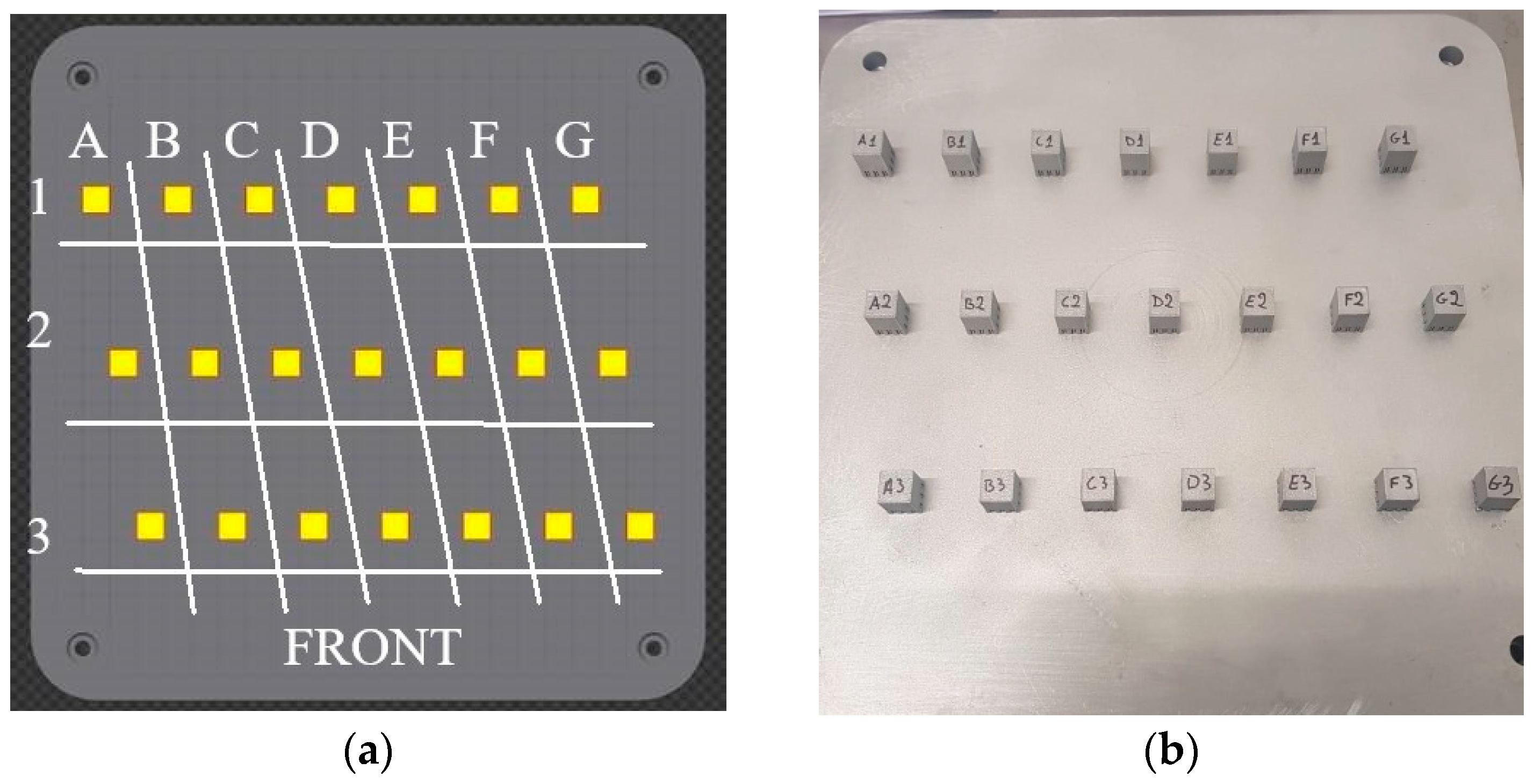
Cube samples were built using a Renishaw AM 400 machine on gas-atomized powder of an average diameter equal to 40 µm. The Meander strategy was used in the process. After processing a stress relief treatment (300 °C for 2 h) was applied. Figure 1 shows the layout defined for the print process and real samples on the table. Three samples were built for each set of process parameters.
The powder composition is shown in Table 1.
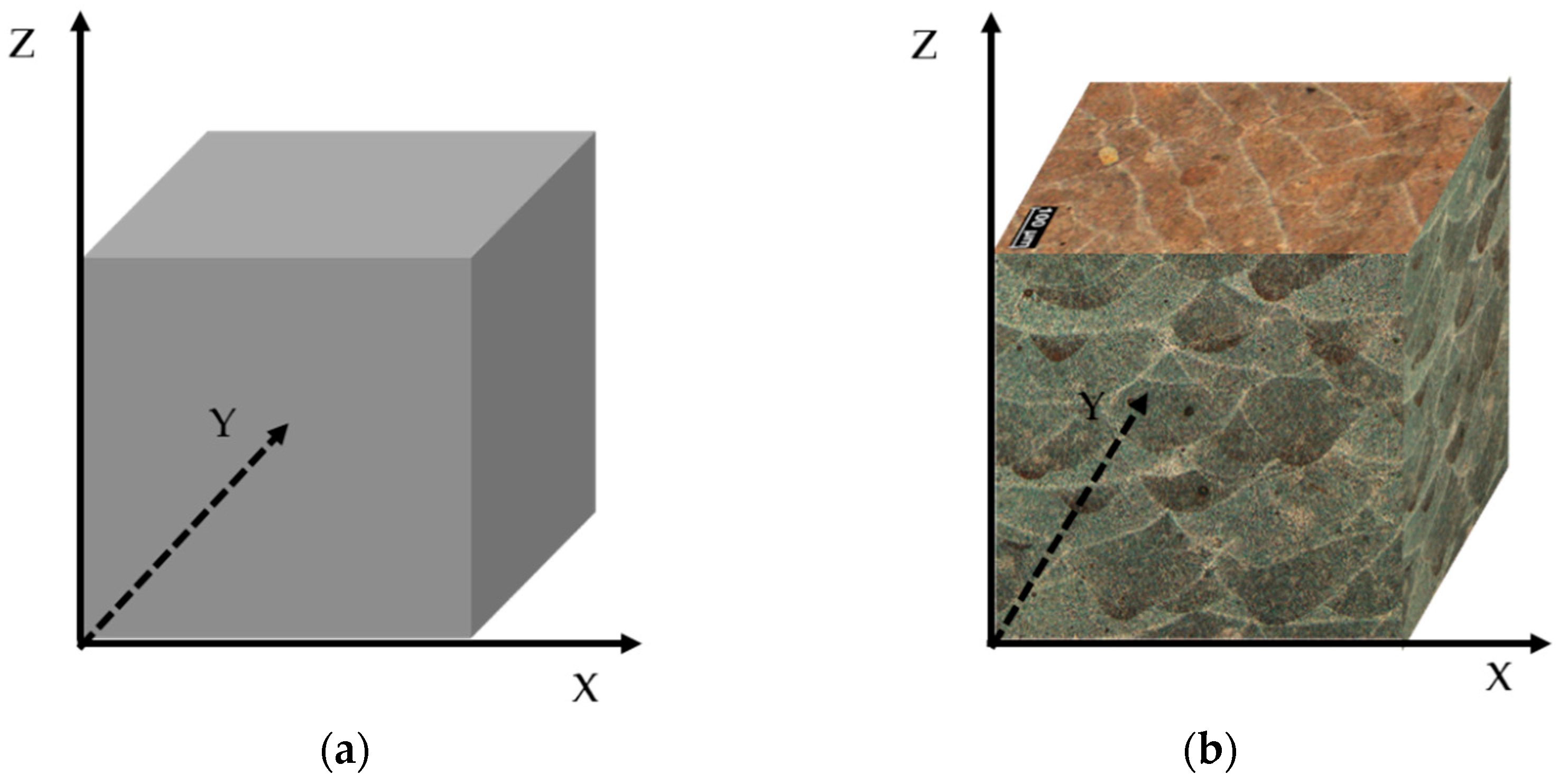
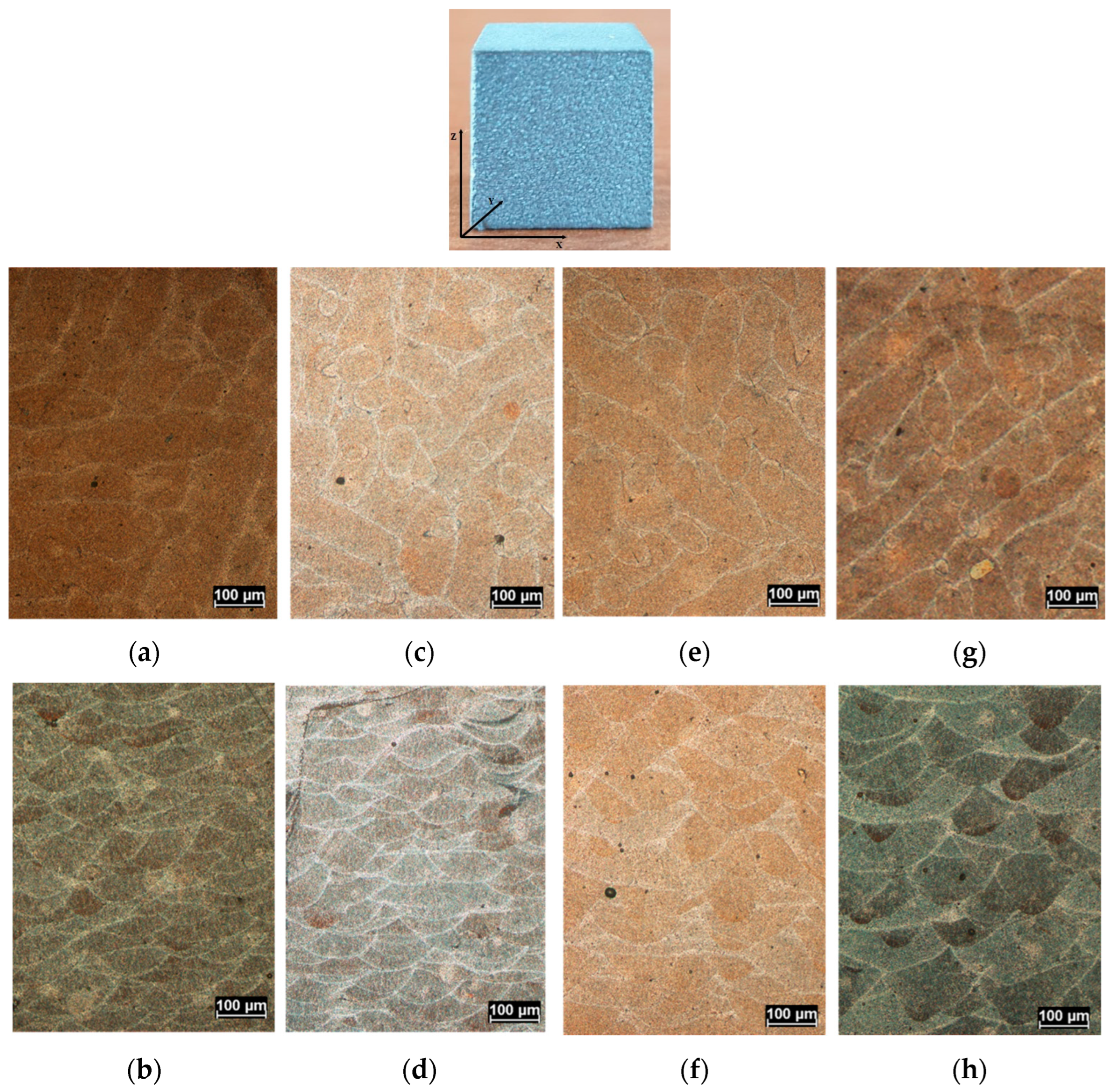
Cube samples with 10 mm edges were built along Z direction (Figure 2a). Moreover, Figure 2b shows the microstructure morphology of the samples processed according to Z direction in the transversal section (XY or T) and in longitudinal sections (XZ and YZ or L).
The building process parameters are shown in Table 2, together with the sample designation. To better recall the samples’ process parameters during the analysis, the samples were named with A or B letters. If processed at 300 W or 350 W, respectively, they were followed by v0, v1, v2, or v3 suffixes, respectively, according to laser scan speeds equal to 1500 mm/s, 1571 mm/s, 1583 mm/s, and 1625 mm/s.
Optical microscope (OM), scanning electron microscope (SEM), and X-ray diffraction (XRD) were used for investigating the microstructure. Particularly, NIKON EPHIPHOT 200 OM, ZEISS EVO SEM equipped with a Bruker energy-dispersive X-ray spectrometer (EDX) and X-ray diffraction Rigaku D/MAX-Ultima X-ray system was employed. Cu (Kα) X-radiation was used.
The sections were prepared following the standard metallographic procedures. For the optical microscope analysis, the microstructure was revealed by Keller etching (95 mL water, 2.5 mL HNO3, 1.5 mL HCl, 1.0 mL HF). On the longitudinal (L) sections of the cubic specimens, the average depth and width of the melt pools were evaluated using NIS Nikon software for image analysis, supplied with optical microscope. All the welding pools in the L sections were characterized. SEM and DRX analyses focused on the amount and size of the silicon particles as a function of the different process parameters.
The fraction of defectiveness area (sum of the area of the defect divided by the section area) was determined on XY and XZ sections by using both Image J software and supplied average values. The defectiveness volume (sum of the volume of the defect divided by the sample volume) was determined by X-ray computed tomography (micro—CT). The lower limit of detection for Image J analysis was taken equal to 20 μm. So, the pores with diameter lower than 20 μm have not been analyzed.
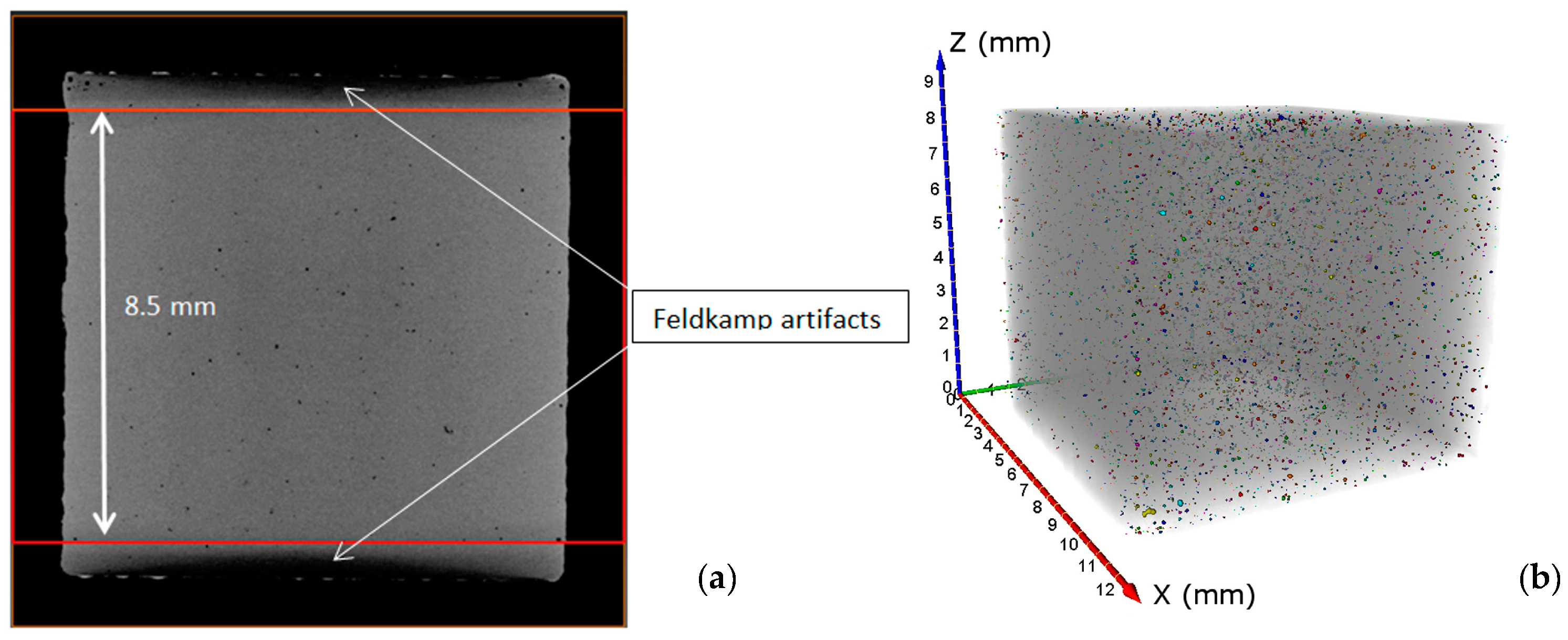
Micro-CT is able to provide information on the internal structure of the analyzed objects as well as on their outer surfaces, by exploiting the properties of penetrating X-rays. The micro-CT analyses were performed by means of a GE Phoenix Nanotom CT system equipped with a 180 kV/15 W nanofocus X-ray tube, a precision rotary table on air bearings, and a 2300 × 2300 pixels Hamamatsu flat panel detector. The CT scan acquisition parameters were properly set before starting the actual X-ray scanning (Table 3), in order to obtain the best 2D X-ray images and consequently a good quality in the tomographic reconstruction. Pores with volume less than 8.0 × 10⁻⁶ mm3 (2 × 2 × 2 = 8 voxels) were excluded from the porosity evaluation to avoid the pixel noise contribution. Once the pores were detected, the porosity was calculated as the ratio between the sum of their volumes and the total volume of the sample. The total examined volume was slightly lower than that of the entire sample (about 0.85 cm3 vs. 1.0 cm3) in order to avoid the Feldkamp effect, a phenomenon of degradation of the intensity values as shown in Figure 3, where, moreover, the volume rendering for the sample Av3 is shown.
HV hardness was measured using a Vickers Affri Wiky 200JS digital instrument employing 0.1 Kg. for holding time equal to 15 s (HV01/15), according to Vickers Hardness ISO 6507-1 (2018) standard.Average hardness values were calculated from edge-to-edge indentation in perpendicular direction, cutting the center of the section 100 µm far from each other on T and L sections.
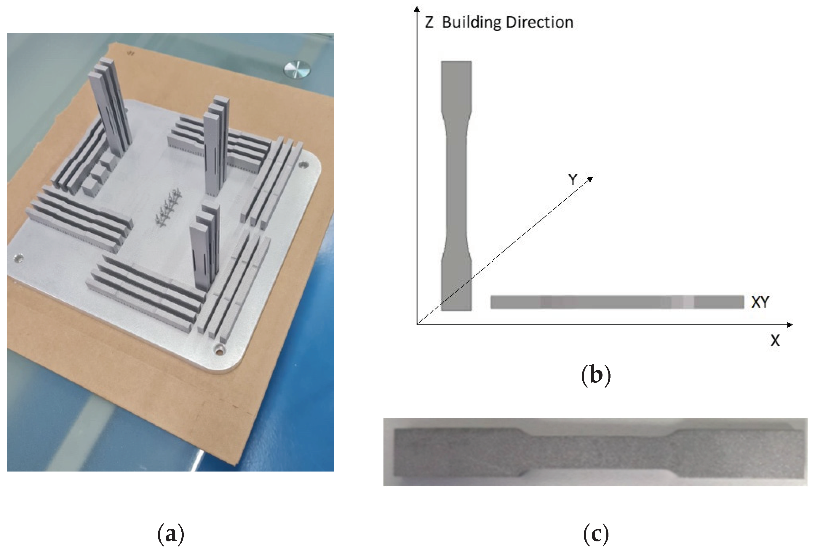
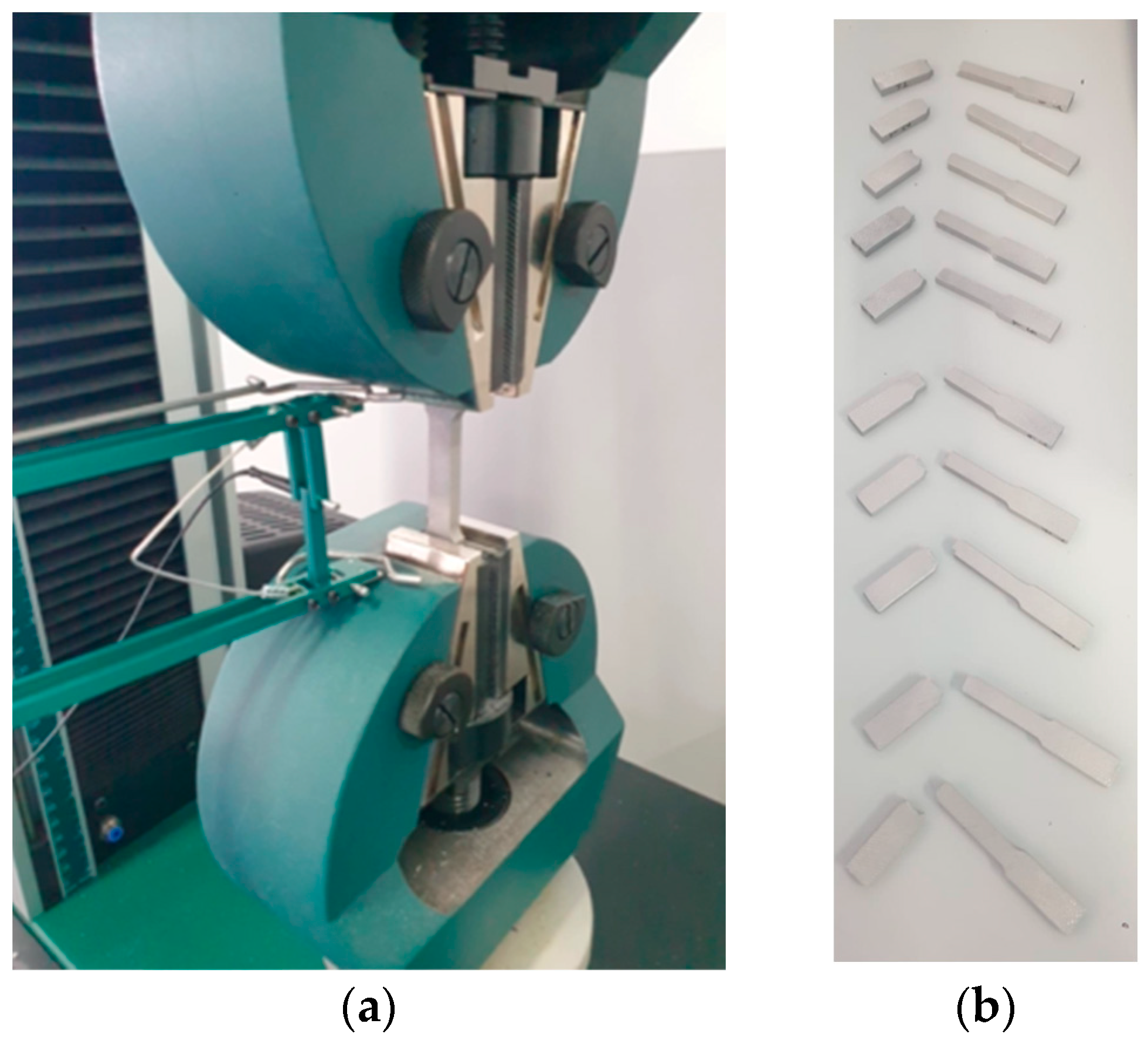
Tensile tests were performed on samples built according to scheme shown in Figure 4a. For each building condition, three samples were built. The XY sample (Figure 4b) has been built perpendicular to the longitudinal section (LS) of the sample shown in Figure 4c. The Z sample has been built perpendicular to its short transverse section (STS) as shown in Figure 4b. While XZ sample has been built perpendicular to its long transverse section (LTS). The tensile test was performed according to ASTM D638—99 standards on a 50 ST Series Universal Testing Machine, Tinius Olsen Inc., with 50 kN capacity (Figure 5a).
3. Results
3.1. Microstructure
The microstructure of the cube sample as analyzed from the optical microscope is shown in Figure 6 for the transversal XZ and longitudinal XY sections of the samples.
In all the sections, the melting pool boundary is clearly observable and lighter after chemical etching. On the transversal sections, the elongated shape of the melting pool (tracks shape) is sometimes interrupted by an almost circular melting zone, which is smaller. Those discontinuities are due to the remelting of the melting tracks when the successive layers have been processed [20].
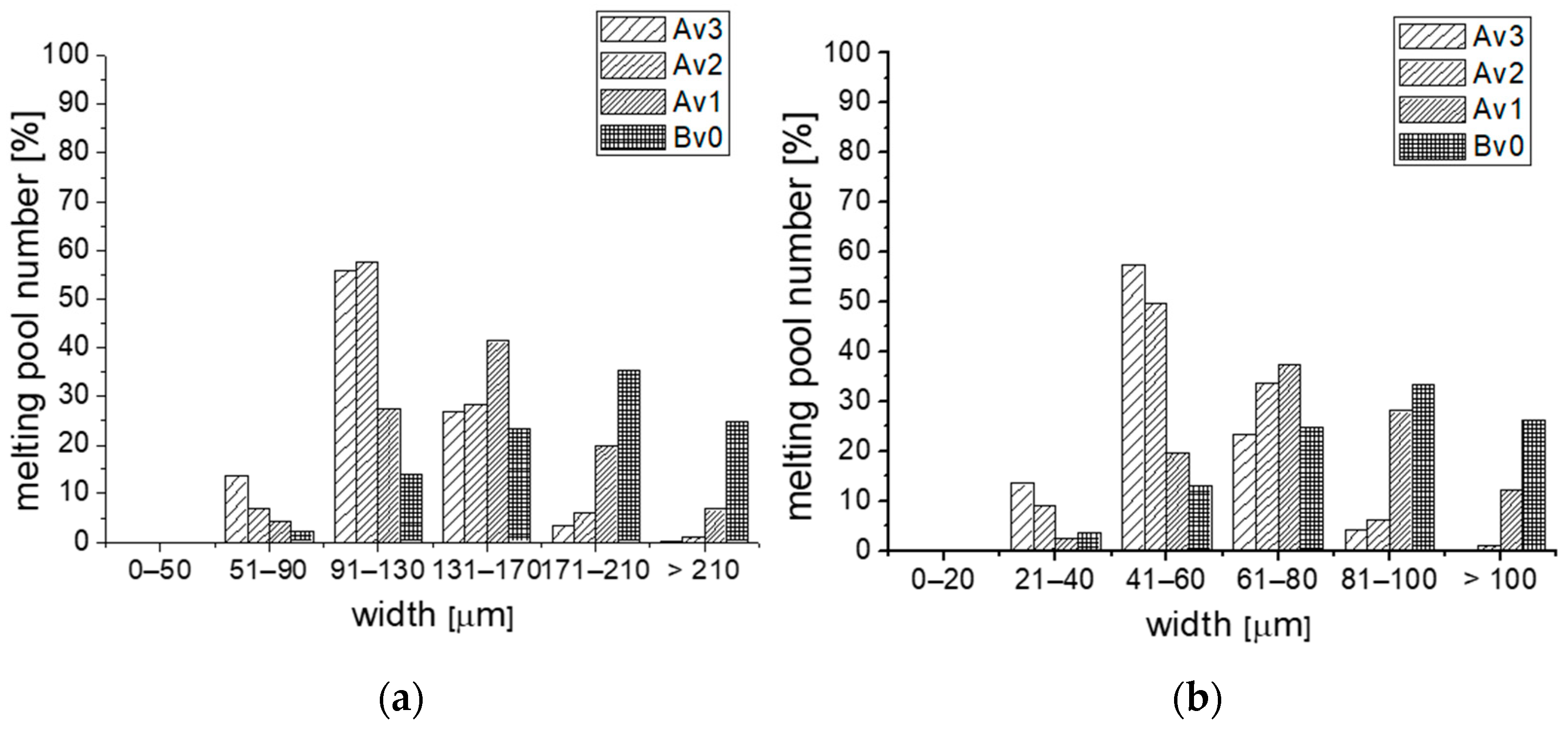
The longitudinal sections show a quite semicircular shape of the melting pool being characterized both by layer-layer and track-track boundaries. The track-track boundaries are can be observed between adjacent melting pools, while the layer-layer boundaries originate from the melting of the powder (this gives the characteristic semi-spherical shape of the molten pool in conduction mode) and remelting of the previous solidified melting pool (which also gives a curved shape to the top of the melting pool) [21]. The role of the different process parameters on melting pool size has been analyzed in Figure 7, where the distribution of the width and depth are shown. Considering the samples processed at the same laser power (A samples), as the scan speed is reduced (Av1 sample), the width and depth of the melting pool increase. Indeed, as the scanning speed is reduced, the net heat input rises and so the size of the melting pool increases. Since the heat input is maximum for the Bv0 sample, this sample exhibits the highest number of melting pools characterized by the highest width and depth. In addition, for the closest values of energy density (Av1 and Av2), similar-sized melting pools should be provided. However, this does not happen (Figure 7a,b). On the contrary, the melting pool sizes are similar for Av2 and Av3 samples but are more different in terms of heat input. This result could be due to the imposed ET in Av2. In fact, the exposure time is lower for Av2 than Av1, and a loss of energy is expected in that sample. For the same reason, the sizes of the melting pools for the Av2 sample are quite similar to those of the Av3 sample, which is characterized by the lowest energy density but the highest ET (that reduces the loss of energy).
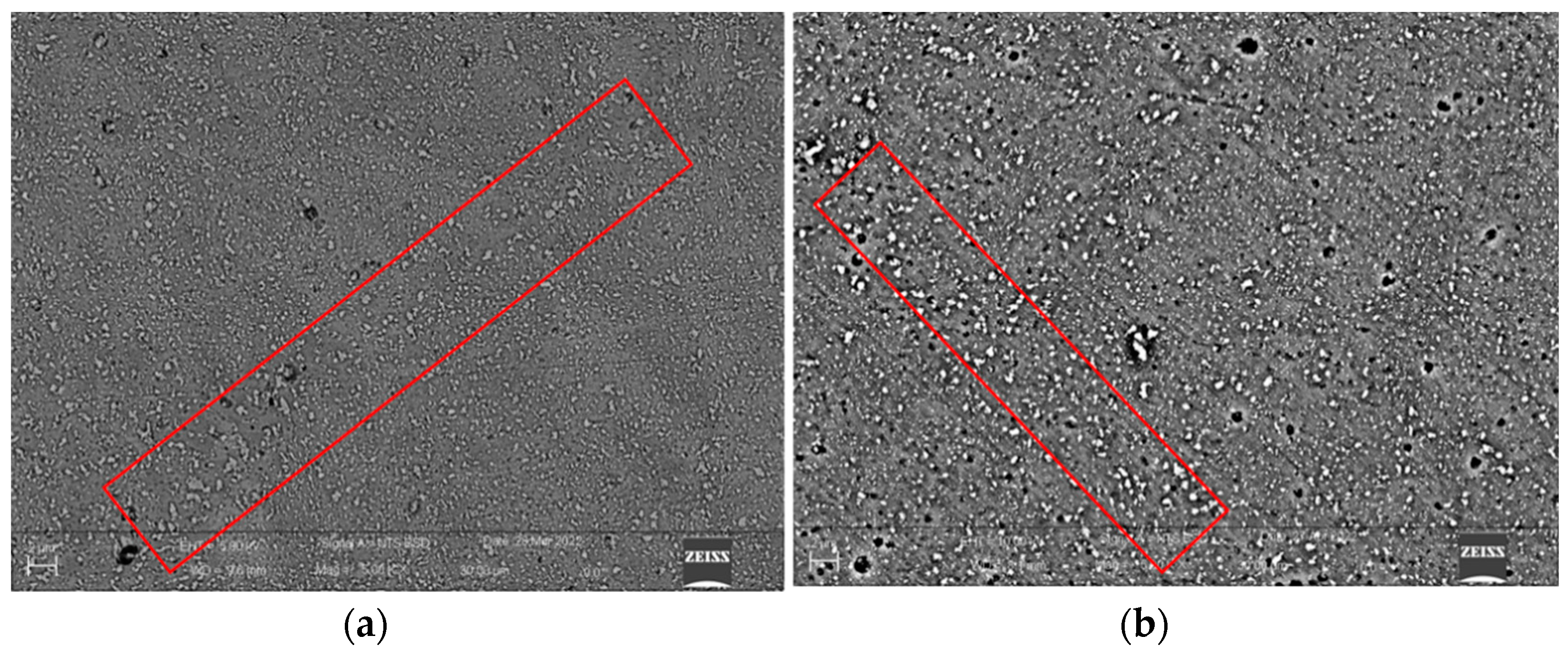
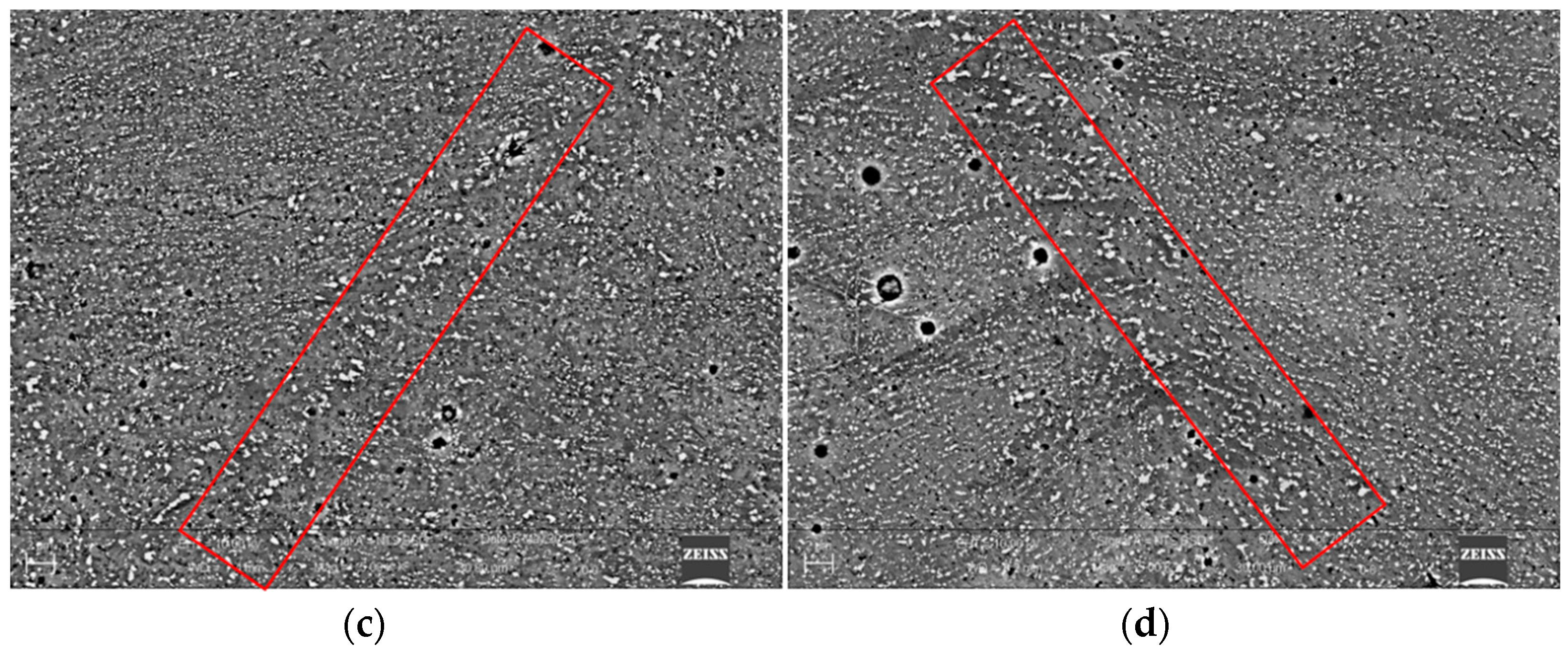
The role of heat input on the related microstructure has been also analyzed in Figure 8. Figure 8 shows the microstructure of samples analyzed from an SEM microscope. In the figure, a gray matrix with dispersed white particles can be observed. The gray matrix is an aluminum solid solution, while the white particles are eutectic Si-Al compounds. At the melting pool boundary (highlight in the red rectangular) a coarser distribution of the silicon phase can be observed, while in the inner of the melting pool, the silicon-phase distribution is finer. The coarser distribution of silicon particles can be explained by different equally valid theories, such as the remelting theory [22] for which the area adjacent to the fusion line is overheated, which is caused by the thermal effect leading to a coarser zone, but it can also be explained by the undercooling theory [23] and the thixo theory [20]. Anyway, as the size of the melting pool increases with energy density (Figure 7a,b), a coarser microstructure is obtained at the melting pool boundaries (Figure 8c,d). The microstructure inside the melting pool, away from the fusion line, is mainly fine cellular [22]. Moreover, even inside the melting pool, a different amount of Si phase precipitating at cell boundary can be observed. Just a qualitative analysis leads to show that as the size of the melting pool decreases for Av3 and Av2 samples (Figure 7a,b), the cell boundary Si phase also decreases due to the faster cooling rate (Figure 8c,d). So, both at the boundary of the melting pool and inside, the amount of Si phase reduces with the energy density.
Therefore, the role of exposure time on the loss of energy is highlighted also in the SEM analysis being the microstructure more similar for the couple Av2 and Av3 than for the couple Av1 and Av2 processed at a very similar value of VED. Moreover, the Av1 microstructure is similar to that of Bvo despite the more significant difference in VED values.
According to a previous study [22], the same happens to secondary Si nanoparticles precipitated from the matrix after that the solidification is completed and upon cooling of the solidified microstructure. Particularly Wang et al. [22] found that nanoparticles of Si occur in the as-built matrix due to solid-state precipitation during the cooling of the melting pool and that the particle size increases with a reduced cooling rate or coarse microstructure.
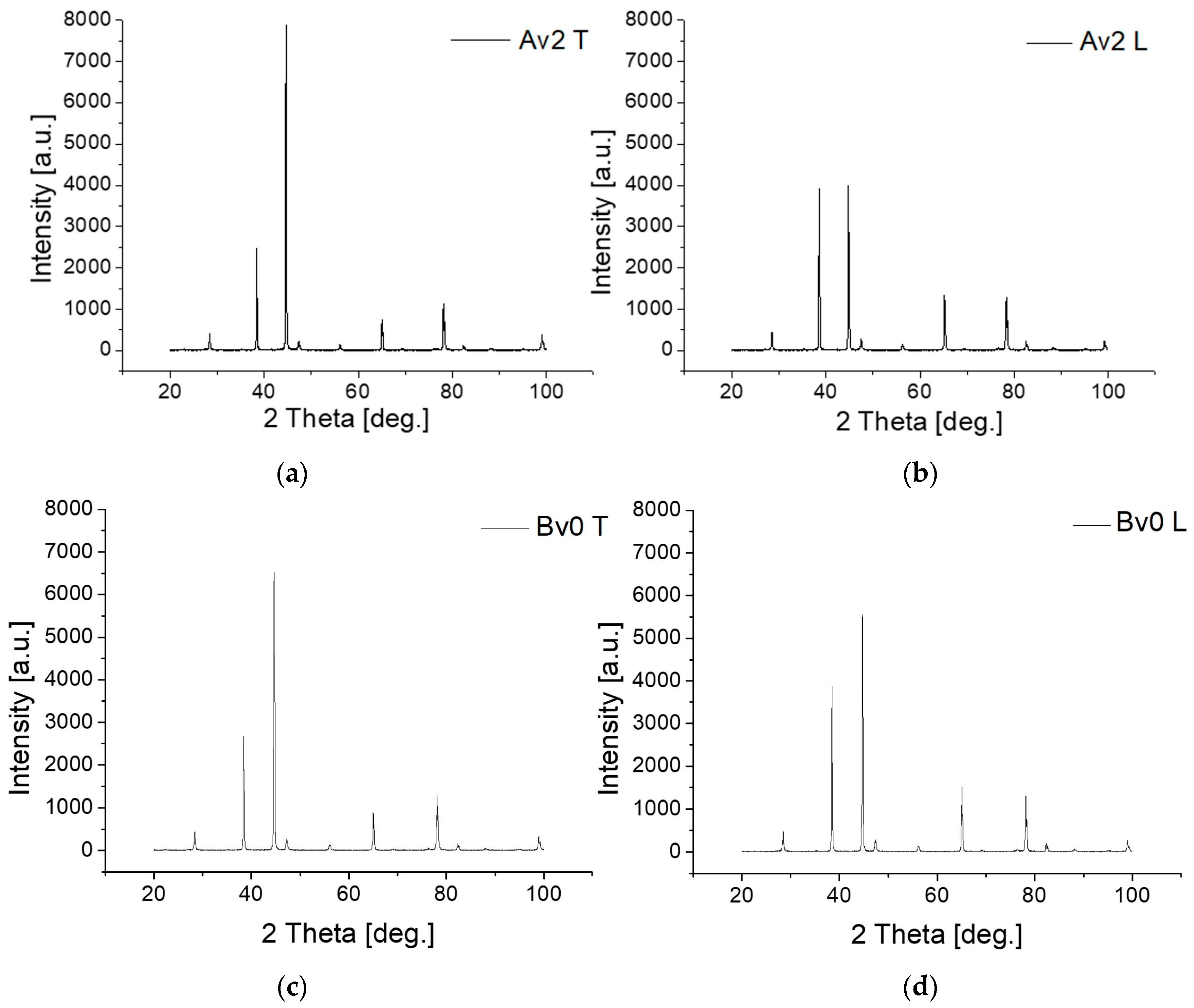
The analysis of the microstructure has been completed and verified by DRX analysis. DRX analysis on both longitudinal and transversal sections of the sample confirms the occurrence of the Si peaks together with the Al ones (Table 4). The Al peaks exhibit the highest intensity (Figure 9). All the peaks have been indexed in Table 4 [24].
Figure 9 also shows the DRX results for the transversal and longitudinal sections of the Av2 and Bv0 samples. In all the patterns, the strongest peak is Al (200) instead of Al (111) and, moreover, this feature is particularly evident in the transverse cross-section (Figure 6a,c). This strongest peak is due to the favorite growth direction of the grain that is <200>, and the slightly different texture in transversal and longitudinal sections is due to the fact that in the transversal section the <200> orientation is dominant, as detailed in [24].
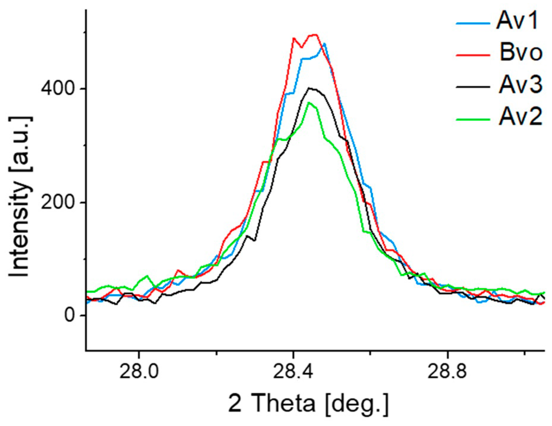
The Av2 and Bv0 samples show a slight difference in the intensity of the Si peaks, particularly the main one (2θ = 28.44) which is more intense for Bv0 samples, as revealed by the previous microstructure analysis (Figure 8 and Figure 9). The main Si peak has been compared to all the analyzed samples and is shown in Figure 10. The analysis of Figure 8 confirms that the amount of Si phase increases in the samples processed with higher energy density (Av1 and Bv0) while is lower in the other ones (Av3 and Av2) as shown in Figure 10. These results agree with the principle of the Rosenthal heat flow theory. In fact, the Rosental equation of heat flow predicts that as the melting pool size increases (Av1 and Bv0), the cooling rate decreases. As a consequence of the reduced cooling rate, lower supersaturation of Si is distributed in the Al matrix as a solid solution and therefore a higher amount of the Silicium phase is obtained in Av1 e Bvo samples.
Table 5 shows the average hardness values in both transversal and longitudinal sections of the samples. The hardness is not much different in all the samples, so they cannot be representative of the microstructure features discussed above. For example, a lower value of hardness should expect in Bv0 samples due to coarser microstructure and the lower supersaturation of the matrix. In fact, the main hardening effect in SLM samples is due to supersaturation according to the constitutive analysis proposed by Shercliff and Ashby [24] and supersaturation decreases at higher energy density according to the reduced cooling rate predicted by the Rosenthal theory. Thus, the average hardness has to be affected by microstructural characteristics which have not been taken into account, such as defectiveness.
3.2. Defectiveness
To clarify the hardness results, porosity has been analyzed in the samples both by CT and optical microscope analysis supported by ImageJ software. The CT results are shown in Table 6.
The level of porosity according to CT analysis decreases significantly in Bvo (4.1%) and Av1 (5.6%) samples with respect to Av2 and Av3 values that are more similar (11.5% and 15.6%, respectively). Moreover, as observed in the microstructural analysis results, Av2 defectiveness level is much higher than Av1 level (despite the very close VED values) both in terms of number (27.3 K vs. 13.8 K) and size distribution. Av1 and Bvo samples, on the contrary, exhibit very close values of defectiveness, although the energy densities are the most different.
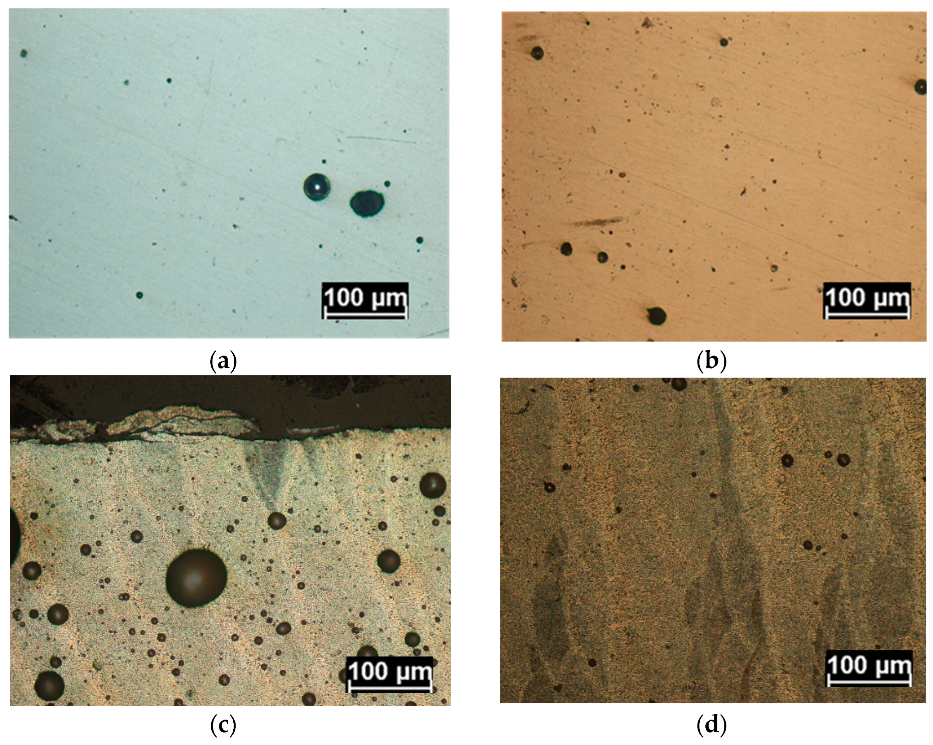
The porosity morphology is mainly spherical (Figure 11). This morphology is usually related to the gas into powder particle gaps, balling phenomenon, and water absorption of aluminum powder due to the significant differences in hydrogen solubility in the solid and liquid phases [4,10,25,26,27]. This type of porosity increases with insufficient energy density because lower values of the heat input favor the balling phenomenon and entrap the bubble of gas in the melting pool. CT results (Table 6) show that the level of porosity decrease with increasing energy density in agreement with the previous studies [4,10,25] and that the highest defectiveness was found in the Av2 sample.
So, despite a high (/low) value of heat input, a lower (/high) hardness should be expected due to the coarser (/finer) microstructure and the lower (/higher) supersaturation of the matrix, also a lower (/higher) level of porosity occurs in the samples. So, the proper microstructure softening (/hardening) is counterbalanced by the opposite effects due to the reduction (/increase) in porosity levels, and therefore no significant difference in hardness can be observed (Table 5).
According to an optical microscope in all the analyzed sections, the amount of defectiveness was always higher and close to the edge of the section with respect to the inner side (Figure 12). Koutiri et al. [25] found that this phenomenon is due to the variation of scan speed near the edge that leads to a deeper melting pool and also favor gas/vapor entrapment. This phenomenon is highlighted in Figure 11c,d on the L sections after chemical etching where deeper melting pools have been observed close to the edge in agreement with Koutiri analysis [25]. Moreover, the shape of the melting pool changes close to the edge, indicating that the heat flow could not mainly be governed by the conduction mode.
Considering the porosity analysis by optical microscopy (Figure 12), a good agreement with the porosity trend released by CT has been found for the analyzed transversal sections (Figure 12a) and also in the longitudinal sections except for the Av2 sample (Figure 12b). In fact, in the analyzed longitudinal sections of Av2 sample, the lowest porosity level has been found (Figure 12b). This result is significant according to the author’s opinion because it highlights the fact that the area percentage of porosity could not be representative of the actual quality of the samples in terms of defectiveness as it results from CT. Anyway, for the other samples in both T and L sections, optical analysis has shown good agreement with the CT trend.
3.3. Tensile Tests
Tensile tests were performed on Av2 and Bvo samples that exhibited the most different microstructure and defectiveness levels. Figure 13 shows the Ultimate Tensile Strength (UTS) and elongation results for the samples processed according to the scheme in Figure 4. Three tests have been performed for each built configuration (XY, XZ, and Z) and each test has been identified with a progressive number close to the built configuration (for example XY1, XY2, and XY3 for the XY configuration and so on) as shown in Figure 13. All the samples exhibit poor elongation varying between 1% and 1.6% for both Av2 and Bvo samples, as shown in Figure 13b. The strength response exhibits a certain difference between Av2 and Bvo samples. In particular, the strength of the Av2 sample is usually higher than that of the Bvo sample except in the case of the Z1 and Z2 samples. The coarser melting pool and Si particle distribution are responsible for the lower tensile properties of the Bv0 samples despite the fact that a lower amount of defectiveness is expected in Bv0 samples, according to the previous characterization.
Moreover, both Av2 and Bv0 samples in the XZ configuration develop higher strength with respect to the Z configuration. The different behavior could be explained in terms of the orientation of the melting pool interfaces with respect to the axis of tensile loading. For the Z specimens, the weak track boundaries are perpendicular to the tensile load direction, providing easier paths for void growth and coalescence. In the horizontal samples, these boundaries are parallel to the loading axis and retard the opening and expansion of voids. As a consequence, a reduction in ductility has been observed for the Z-built Av2 samples, while, in terms of ductility, the results are less obvious for the Z-built Bv0 samples and require further investigation [28]. In any case, the values of the tensile strengths are always higher with respect to those of the alloy processed according to conventional casting processes [8], but the elongations are lower.
4. Conclusions
In this study, the microstructural evolutions, defectiveness, and mechanical properties of SLM Al-Si10-Mg samples processed at very close values of heat input have been characterized.
The main conclusions are summarized as follows:
- (1)
- The size of the melting pool increases with energy density. Anyway, the closest values of energy density (70,175.4 J/mm3 and 70,707.1 J/mm3) do not lead to the most similar melting pool sizes. This result could be due to the exposure time effect (40 μs at 70,175.4 J/mm3 and 50 μs at 70,707.1 J/mm3, respectively) on the energy losses. Specifically, the energy losses are increased as the exposure time decreases, leading to a smaller melting pool size.
- (2)
- The amount of Si phase increases in energy density equal to or higher than 70,707.1 J/mm3. Specifically, starting from that level of energy density, a significant increase in the size of the melting pool has been observed, leading to a lower cooling rate and matrix supersaturation. So, the amount of Silicium second phase is increased.
- (3)
- The porosity of the samples is mainly spherical and the lowest value of porosity, equal to 4.1% was found in the sample processed at the highest energy density (86,419.8 J/mm3). Anyway, the closest values of energy density (70,175.4 J/mm3 and 70,707.1 J/mm3) do not lead to the most similar porosity level. Additionally, this result could be due to the exposure time effect (40 μs at 70,175.4 J/mm3 and 50 μs at 70,707.1 J/mm3, respectively) on the energy losses. In particular, the porosity level was found equal to 15.6% for 40 μs and 5.6% for 50 μs. Moreover, the level of porosity was always found to be higher and close to the edge of both transversal and longitudinal sections.
- (4)
- The hardness values of the samples do not differ significantly. This is probably because the finer microstructure related to the lower values of energy density (70,175.4 J/mm3 and 68,376.1 J/mm3) that should lead to a higher hardness is counterbalanced by the highest level of defectiveness in those samples.
- (5)
- Tensile tests have shown poor ductility for the samples. In particular, the coarser microstructure of the samples processed at the highest energy density (86,419.8 J/mm3) leads to lower tensile properties. The tensile test response is always lower for the Z-building configurations.
- (6)
- Taking into account the microstructure features, the amount of defectiveness, and the resulting mechanical properties of all the samples analyzed in this study, the optimal process parameters have been identified to be the following: power 300 W; exposure time 50 μs; point distance 110 μm; hatch distance 0.09 mm; layer thickness of 0.03 mm; and scan speed 1571.4 mm/s.
Author Contributions
Conceptualization, P.L., A.D.P. and T.P.; methodology, P.L., A.D.P., T.P. and M.N.; formal analysis, P.L.; data curation. P.L.; writing—original draft preparation, P.L.; review and editing P.L., A.D.P. and T.P.; supervision, P.L. All authors have read and agreed to the published version of the manuscript.
Funding
Innovative Solutions for the quality and sustainability of ADDitive manufacturing processes—SIADD project, identification code (CUP) B26G18001480005, founded by the Italian Ministry for Education, University and Research within the National Program PON 2014/2020 derived by the European Program Horizon 2020.
Data Availability Statement
Not applicable.
Acknowledgments
The authors thank the HB-Technology company of Taranto (Italy) for their support.
Conflicts of Interest
The authors declare no conflict of interest.
References
- Polmear, I.J. Light Alloys-Metallurgy of the Light Metals, 3rd ed.; Arnold: London, UK, 1995. [Google Scholar]
- Smith, W.F. Structure and Properties of Engineering Alloys, 2nd ed.; McGraw-Hill: London, UK, 1993. [Google Scholar]
- Asphal, Y.; Jawalkar, C.S.; Kant, S. A review on use of aluminium alloys in aircraft components. J. Mater. Sci. 2015, 3, 33–38. [Google Scholar]
- Zhang, J.; Song, B.; Wei, Q.; Bourell, D.; Shi, Y. A review of selective laser melting of aluminum alloys: Processing, microstructure, property and developing trends. J. Mater. Sci. Technol. 2019, 35, 270–284. [Google Scholar] [CrossRef]
- Aboulkhair, N.T.; Simonelli, M.; Parry, L.; Ashcroft, I.; Tuck, C. 3D printing of Aluminium alloys: Additive Manufacturing of Aluminium alloys using selective laser melting. Prog. Mater. Sci. 2019, 106, 100578. [Google Scholar] [CrossRef]
- Olakanmi, E.O.; Cochrane, R.F.; Dalgarno, K.W. Densification mechanism and microstructural evolution in selective laser sintering of Al–12Si powders. J. Mater. Process. Technol. 2011, 211, 113–121. [Google Scholar] [CrossRef]
- Chen, B.; Moon, S.; Yao, X.; Bi, G.; Shen, J.; Umeda, J.; Kondoh, K. Strength and strain hardening of a selective laser melted AlSi10Mg alloy. Scr. Mater. 2017, 141, 45–49. [Google Scholar] [CrossRef]
- Kempen, K.; Thijs, L.; Van Humbeeck, J.; Kruth, J.-P. Mechanical Properties of AlSi10Mg Produced by Selective Laser Melting. Phys. Procedia 2012, 39, 439–446. [Google Scholar] [CrossRef] [Green Version]
- Roehling, J.D.; Coughlin, D.R.; Gibbs, J.W.; Baldwin, J.K.; Mertens, J.C.E.; Campbell, G.H.; Clarke, A.J.; McKeown, J.T. Rapid solidification growth mode transitions in Al-Si alloys by dynamic transmission electron microscopy. Acta Mater. 2017, 131, 22–30. [Google Scholar] [CrossRef] [Green Version]
- Maskery, I.; Aboulkhair, N.T.; Corfield, M.R.; Tuck, C.; Clare, A.T.; Leach, R.K.; Wildman, R.D.; Ashcroft, I.A.; Hague, R.J.M. Quantification and characterisation of porosity in selectively laser melted Al–Si10–Mg using X-ray computed tomography. Mater. Charact. 2016, 111, 193–204. [Google Scholar] [CrossRef] [Green Version]
- Wu, J.; Wang, X.Q.; Wang, W.; Attallah, M.M.; Loretto, M.H. Microstructure and strength of selectively laser melted AlSi10Mg. Acta Mater. 2016, 117, 311–320. [Google Scholar] [CrossRef] [Green Version]
- Ciurana, J.; Hernandez, L.; Delgado, J. Energy density analysis on single tracks formed by selective laser melting with CoCrMo powder material. Int. J. Adv. Manuf. Technol. 2013, 68, 1103–1110. [Google Scholar] [CrossRef]
- Gunenthiram, V.; Peyre, P.; Schneider, M.; Dal, M.; Coste, F.; Koutiri, I.; Fabbro, R. Experimental analysis of spatter generation and melt-pool behavior during the powder bed laser beam melting process. J. Mater. Process. Technol. 2018, 251, 376–386. [Google Scholar] [CrossRef]
- Bertoli, U.S.; Wolfer, A.J.; Matthews, M.J.; Delplanque, J.-P.R.; Schoenung, J.M. On the limitations of Volumetric Energy Density as a design parameter for Selective Laser Melting. Mater. Des. 2017, 113, 331–340. [Google Scholar] [CrossRef] [Green Version]
- Riquelme, A.; Rodrigo, P.; Escalera-Rodriguez, M.D.; Rams, J. Effect of the process parameters in the additive manufacturing of in situ Al/AlN samples. J. Manuf. Process. 2019, 46, 271–278. [Google Scholar] [CrossRef]
- Messler, R.W., Jr. Principles of Welding: Processes, Physics, Chemistry, and Metallurgy; Wiley: New York, NY, USA, 1999. [Google Scholar]
- Porter, D.A.; Easterling, K.E. Phase Transformations in Metals and Alloys; CRC Press: Boca Raton, FL, USA, 1992. [Google Scholar]
- Thijs, L.; Kempen, K.; Kruth, J.-P.; Van Humbeeck, J. Fine-structured aluminium products with controllable texture by selective laser melting of pre-alloyed AlSi10Mg powder. Acta Mater. 2013, 61, 1809–1819. [Google Scholar] [CrossRef] [Green Version]
- Aboulkhair, N.T.; Everitt, N.M.; Ashcroft, I.; Tuck, C. Reducing porosity in AlSi10Mg parts processed by selective laser melting. Addit. Manuf. 2014, 1–4, 77–86. [Google Scholar] [CrossRef]
- Liu, X.; Zhao, C.; Zhou, X.; Shena, Z.; Liu, W. Microstructure of selective laser melted AlSi10Mg alloy. Mater. Des. 2019, 168, 107677. [Google Scholar] [CrossRef]
- Patakham, U.; Palasay, A.; Wila, P.; Tongsri, R. MPB characteristics and Si morphologies on mechanical properties and fracture behavior of SLM AlSi10Mg. Mater. Sci. Eng. A 2021, 821, 141602. [Google Scholar] [CrossRef]
- Wang, L.-Z.; Wang, S.; Hong, X. Pulsed SLM-manufactured AlSi10Mg alloy: Mechanical properties and microstructural effects of designed laser energy densities. J. Manuf. Process. 2018, 35, 492–499. [Google Scholar] [CrossRef]
- Li, W.; Li, S.; Liu, J.; Zhang, A.; Zhou, Y.; Wei, Q.; Yan, C.; Shi, Y. Effect of heat treatment on AlSi10Mg alloy fabricated by selective laser melting: Microstructure evolution, mechanical properties and fracture mechanism. Mater. Sci. Eng. A 2016, 663, 116–125. [Google Scholar] [CrossRef]
- Zhou, L.; Mehta, A.; Schulz, E.; McWilliams, B.; Cho, K.; Sohn, Y. Microstructure, precipitates and hardness of selectively laser melted AlSi10Mg alloy before and after heat treatment. Mater. Charact. 2018, 143, 5–17. [Google Scholar] [CrossRef]
- Koutiri, I.; Pessard, E.; Peyre, P.; Amlou, O.; De Terris, T. Influence of SLM process parameters on the surface finish, porosity rate and fatigue behavior of as-built Inconel 625 parts. J. Mater. Process. Technol. 2018, 255, 536–546. [Google Scholar] [CrossRef]
- Baitimerov, R.; Lykov, P.; Zherebtsov, D.; Radionova, L.; Shultc, A.; Prashanth, K.G. Influence of Powder Characteristics on Processability of AlSi12 Alloy Fabricated by Selective Laser Melting. Materials 2018, 11, 742. [Google Scholar] [CrossRef] [Green Version]
- Kempen, K.; Thijs, L.; Yasa, E.; Badrossamay, M.; Verheecke, W.; Kruth, J.-P. Process optimization and microstructural analysis for selective laser melting of AlSi10Mg. In Proceedings of the 2011 International Solid Freeform Fabrication Symposium, Austin, TX, USA, 8–10 August 2011. [Google Scholar] [CrossRef]
- Yadollahi, A.; Shamsaei, N.; Thompson, S.M.; Elwany, A.; Bian, L. Effects of building orientation and heat treatment on fatigue behavior of selective laser melted 17-4 PH stainless steel. Int. J. Fatigue 2017, 94, 218–235. [Google Scholar] [CrossRef]
Figure 1.
Layout of the samples (a); real samples on the table (b).

Figure 2.
Building direction of the cubic sample (Z) (a); scheme of sample microstructure along T and L sections (b).
Figure 2.
Building direction of the cubic sample (Z) (a); scheme of sample microstructure along T and L sections (b).

Figure 3.
Size of XZ section in order to avoid Feldkamp effect (a); volume rendering of the sample Av3 (b) showing the detected porosity.
Figure 3.
Size of XZ section in order to avoid Feldkamp effect (a); volume rendering of the sample Av3 (b) showing the detected porosity.

Figure 4.
Building process layout (a); building direction of test samples (b); a real tensile sample (c).
Figure 4.
Building process layout (a); building direction of test samples (b); a real tensile sample (c).

Figure 5.
Tensile Testing Machine with the sample (a); some of the samples tested (b).

Figure 6.
Optical micrographs of the traversals XZ section (a,c,e,g) and longitudinal XY sections (b,d,f,h) for the sample Av3 (a,b) Av2 (c,d) Av1 (e,f) and Bv0 (g,h).
Figure 6.
Optical micrographs of the traversals XZ section (a,c,e,g) and longitudinal XY sections (b,d,f,h) for the sample Av3 (a,b) Av2 (c,d) Av1 (e,f) and Bv0 (g,h).

Figure 7.
Distribution of the melting pool width (a) and depth (b) for Av3, Av2, Av1 and Bv0 samples.
Figure 7.
Distribution of the melting pool width (a) and depth (b) for Av3, Av2, Av1 and Bv0 samples.

Figure 8.
SEM micrographs of the longitudinal sections of the sample Av3 (a) Av2 (b) Av1 (c) and Bv0 (d).
Figure 8.
SEM micrographs of the longitudinal sections of the sample Av3 (a) Av2 (b) Av1 (c) and Bv0 (d).


Figure 9.
DRX pattern for the transversal and longitudinal sections of Av2 (a,b) and Bvo (c,d) samples.
Figure 9.
DRX pattern for the transversal and longitudinal sections of Av2 (a,b) and Bvo (c,d) samples.

Figure 10.
Main Si peak (2θ = 28.44) intensity for the samples.

Figure 11.
Morphology of the voids in T (a,b) and L (c,d) plane of Av3 (a,c) and Bv0 (b,d) samples. Etched microstructure of the L planes close to the edge of the samples (c,d) showing the different morphology of the melting pool with respect to Figure 4.
Figure 11.
Morphology of the voids in T (a,b) and L (c,d) plane of Av3 (a,c) and Bv0 (b,d) samples. Etched microstructure of the L planes close to the edge of the samples (c,d) showing the different morphology of the melting pool with respect to Figure 4.

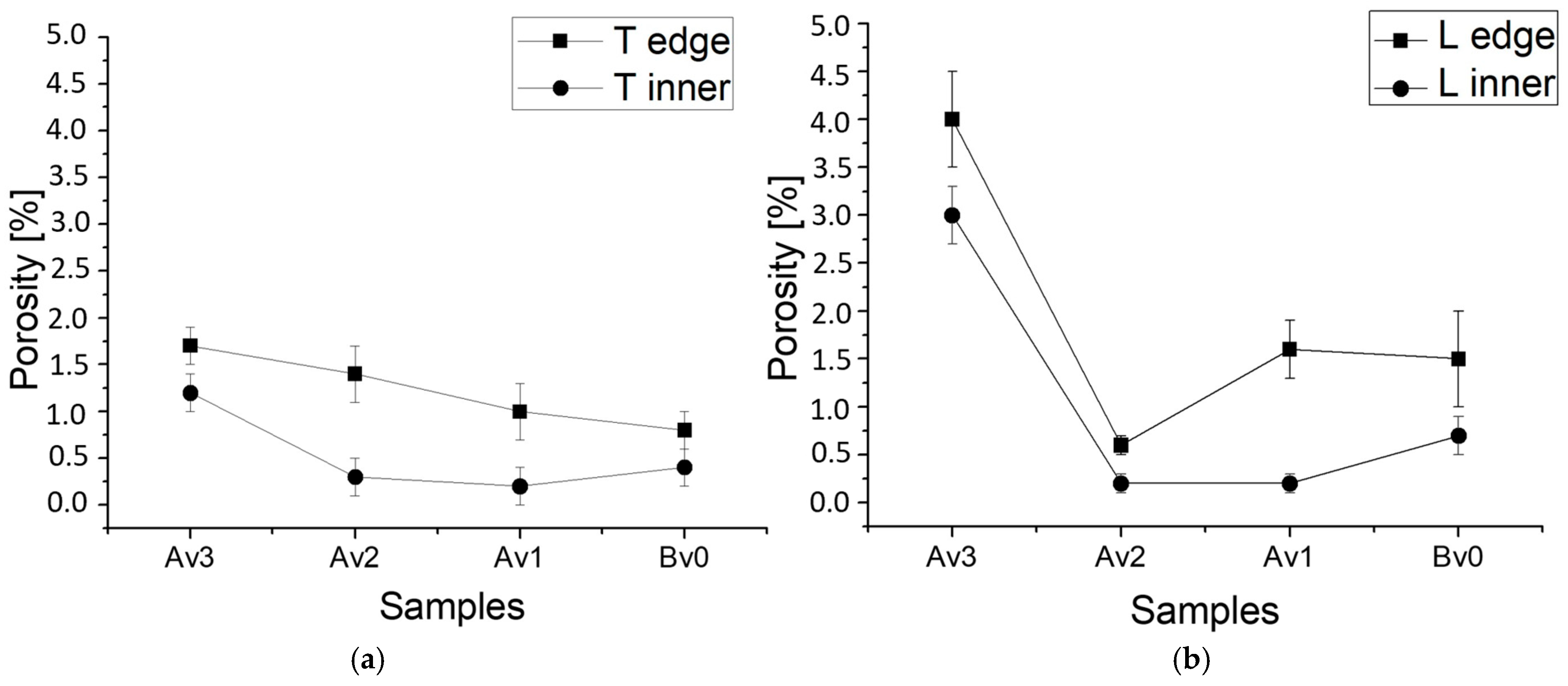
Figure 12.
Porosity percentage evaluated close to the edge of transversal (a); longitudinal sections of the samples and in the inner of the sections (b).
Figure 12.
Porosity percentage evaluated close to the edge of transversal (a); longitudinal sections of the samples and in the inner of the sections (b).

Figure 13.
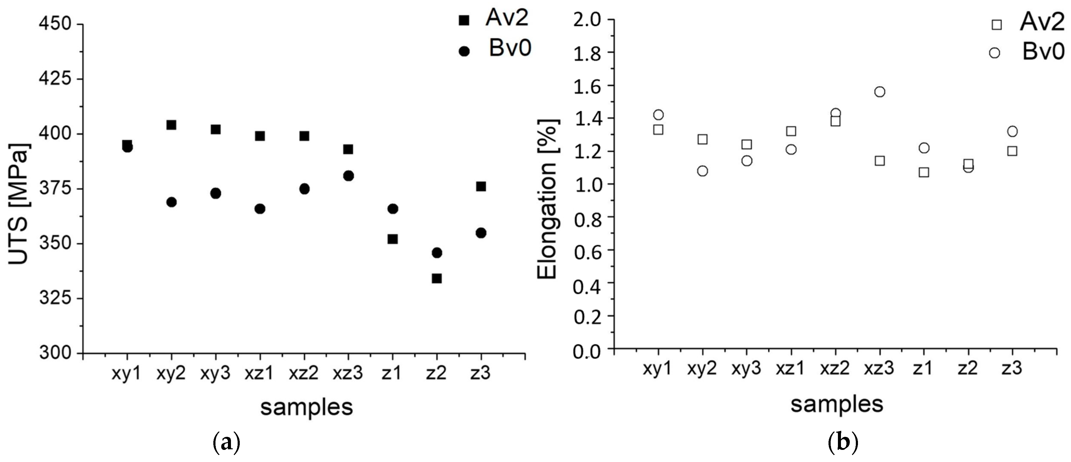
Ultimate tensile strength (a) and elongation (b) values for the different built configurations of the specimen.
Figure 13.
Ultimate tensile strength (a) and elongation (b) values for the different built configurations of the specimen.


Table 1.
Powder composition (wt.%).
| Si | Fe | Cu | Mn | Mg | Cr | Zn | Ti | Al |
|---|---|---|---|---|---|---|---|---|
| 0.80 | 0.40 | 0.10 | 0.50 | 1.2 | 0.30 | 0.20 | <0.15 | bal. |
Table 2.
Samples designation and SLM process parameters.
| Samples Designation | Power (W) | Exposure Time (μs) | TOFF (μs) | Point Distance (μm) | Hatch Distance (mm) | Layer Thickness (mm) | VED (J/mm3) | v (mm/s) | Eline J/mm |
|---|---|---|---|---|---|---|---|---|---|
| Av1 | 300 | 50 | 20 | 110 | 0.09 | 0.03 | 70,707.1 | 1571.4 | 0.1909 |
| Av2 | 300 | 40 | 20 | 95 | 0.09 | 0.03 | 70,175.4 | 1583.3 | 0.1894 |
| Av3 | 300 | 60 | 20 | 130 | 0.09 | 0.03 | 68,376.1 | 1625 | 0.1846 |
| Bv0 | 350 | 40 | 20 | 90 | 0.09 | 0.03 | 86,419.8 | 1500 | 0.233 |
Table 3.
CT experimental conditions.
| Target | Voltage (KV) | Current (μA) | Integration Time (ms) | Resolution (μm) | Number of Radigraphies |
|---|---|---|---|---|---|
| Tungsten | 120 | 80 | 750 | 7.5 | 2000 |
Table 4.
Peak identifications for the spectra shown in Figure 9.
Table 4.
Peak identifications for the spectra shown in Figure 9.
| 2theta [deg] | 28.44 | 38.46 | 44.72 | 47.43 | 56.20 | 65.08 | 78.18 | 82.38 | 99.00 |
|---|---|---|---|---|---|---|---|---|---|
| Peaks identification | Si (111) | Al (111) | Al (200) | Si (220) | Si (331) | Al (220) | Al (311) | Al (222) | Al (400) |
Table 5.
Hardness values in both transversal and longitudinal sections of the sample.
| Samples | HV T 0.1/15 | HV L 0.1/15 | HV Average 0.1/15 |
|---|---|---|---|
| 300 Av3 | 68.8 ± 1.4 | 67.2 ± 1.9 | 68.0 ± 1.6 |
| 300 Av2 | 67.7 ± 1.2 | 64.5 ± 2.4 | 66.1 ± 2.2 |
| 300 Av1 | 68.2 ± 1.7 | 70 ± 1.8 | 69.0 ± 1.4 |
| 350 Bv0 | 68.2 ± 2.2 | 70 ± 2.3 | 69.1 ± 2.3 |
Table 6.
Pore statistics on the samples by CT.
| Samples | Pores Number | Porosity% | Equivalent Diameter (μm) | Volume (mm3) |
|---|---|---|---|---|
| Av3 | 16821 | 0.115 | mean: 39.42 min: 20.05 max: 267.70 | mean: 5.77 × 10⁻⁵ min: 4.22 × 10⁻⁶ max: 10.04 × 10⁻³ |
| Av2 | 27286 | 0.159 | mean: 37.34 min: 20.05 max: 220.36 | mean: 4.94 × 10⁻⁵ min: 4.22 × 10⁻⁶ max: 5.60 × 10⁻³ |
| Av1 | 13785 | 0.056 | mean: 34.79 min: 20.05 max: 165.02 | mean: 3.45 × 10⁻⁵ min: 4.22 × 10⁻⁶ max: 2.35 × 10⁻³ |
| Bv0 | 8287 | 0.041 | mean: 35.97 min: 20.05 max: 139.08 | mean: 4.07 × 10⁻⁵ min: 4.22 × 10⁻⁶ max: 1.41 × 10⁻³ |
Disclaimer/Publisher’s Note: The statements, opinions and data contained in all publications are solely those of the individual author(s) and contributor(s) and not of MDPI and/or the editor(s). MDPI and/or the editor(s) disclaim responsibility for any injury to people or property resulting from any ideas, methods, instructions or products referred to in the content. |
© 2023 by the authors. Licensee MDPI, Basel, Switzerland. This article is an open access article distributed under the terms and conditions of the Creative Commons Attribution (CC BY) license (https://creativecommons.org/licenses/by/4.0/).
Share and Cite
MDPI and ACS Style
Leo, P.; Del Prete, A.; Primo, T.; Nacucchi, M. Al-Si10-Mg Manufactured by Selective Laser Melting: Microstructure Sensitivity to Close Values of the Heat Input. Metals 2023, 13, 590. https://doi.org/10.3390/met13030590
AMA Style
Leo P, Del Prete A, Primo T, Nacucchi M. Al-Si10-Mg Manufactured by Selective Laser Melting: Microstructure Sensitivity to Close Values of the Heat Input. Metals. 2023; 13(3):590. https://doi.org/10.3390/met13030590
Chicago/Turabian StyleLeo, Paola, Antonio Del Prete, Teresa Primo, and Michele Nacucchi. 2023. "Al-Si10-Mg Manufactured by Selective Laser Melting: Microstructure Sensitivity to Close Values of the Heat Input" Metals 13, no. 3: 590. https://doi.org/10.3390/met13030590
Note that from the first issue of 2016, this journal uses article numbers instead of page numbers. See further details here.