Drain Current Stress-Induced Instability in Amorphous InGaZnO Thin-Film Transistors with Different Active Layer Thicknesses


1
Key Laboratory of Applied Surface and Colloid Chemistry, Ministry of Education, Shaanxi Key Laboratory for Advanced Energy Devices, Shaanxi Engineering Lab for Advanced Energy Technology, School of Materials Science and Engineering, Shaanxi Normal University, Xi’an 710119, China
2
School of Environmental Science and Engineering, Kochi University of Technology, Kami, Kochi 782-8502, Japan
3
Center for Nanotechnology in Research Institute, Kochi University of Technology, Kami, Kochi 782-8502, Japan
*
Authors to whom correspondence should be addressed.
Materials 2018, 11(4), 559; https://doi.org/10.3390/ma11040559
Submission received: 21 February 2018
/
Revised: 19 March 2018
/
Accepted: 2 April 2018
/
Published: 5 April 2018
(This article belongs to the Section Thin Films and Interfaces)
Abstract
:In this study, the initial electrical properties, positive gate bias stress (PBS), and drain current stress (DCS)-induced instabilities of amorphous indium gallium zinc oxide (a-IGZO) thin-film transistors (TFTs) with various active layer thicknesses (TIGZO) are investigated. As the TIGZO increased, the turn-on voltage (Von) decreased, while the subthreshold swing slightly increased. Furthermore, the mobility of over 13 cm2·V−1·s−1 and the negligible hysteresis of ~0.5 V are obtained in all of the a-IGZO TFTs, regardless of the TIGZO. The PBS results exhibit that the Von shift is aggravated as the TIGZO decreases. In addition, the DCS-induced instability in the a-IGZO TFTs with various TIGZO values is revealed using current–voltage and capacitance–voltage (C–V) measurements. An anomalous hump phenomenon is only observed in the off state of the gate-to-source (Cgs) curve for all of the a-IGZO TFTs. This is due to the impact ionization that occurs near the drain side of the channel and the generated holes that flow towards the source side along the back-channel interface under the lateral electric field, which cause a lowered potential barrier near the source side. As the TIGZO value increased, the hump in the off state of the Cgs curve was gradually weakened.
1. Introduction
Recently, amorphous indium gallium zinc oxide (a-IGZO), as a representative of an amorphous metal oxide-based semiconductor, has been widely investigated for use in the active layer of thin-film transistors (TFTs) due to its high electron mobility, good transparency in visible light, chemical and thermal stability, low temperature processing, and smooth surface [1,2,3,4]. The a-IGZO TFT with excellent electrical properties, such as high mobility (μ) of over 10 cm2·V−1·s−1 and low values of subthreshold swing, has become one of the research hotspots for the advanced display application in next-generation active-matrix liquid crystal displays (AM-LCDs) and active-matrix organic light-emitting diodes (AM-OLEDs) [5,6,7,8]. Hitherto, AM-OLEDs driven by the a-IGZO TFTs involve two or three transistors and one capacitor current-biased voltage-programmed pixel circuit. Therefore, the stability of the a-IGZO TFTs under long-term current-bias is a critical issue for these circuits in AM-OLEDs. However, the a-IGZO TFTs inevitably suffer gate and drain bias stresses during practical operation conditions, leading to device instability and hindering their development for commercial products [9,10]. Fujii et al. [11] have investigated the increase in internal temperature of the IGZO TFTs when the device was operated in the saturation region. Choi et al. [12] have reported that the electron-hole pair generation by impact ionization near the drain side contributed to the negative shift of the threshold voltage of IGZO TFTs with wide channel width under a high gate and drain bias stress. Valdinoci et al. [13] have reported that the electron-hole pair generation by impact ionization near the drain region caused the floating body effect in high μ poly-Si TFTs. Consequently, the electrical stability under drain current stress was considered to be an important issue, especially for high-μ oxide TFTs.
Moreover, the active layer thickness is an important parameter to adjust device electrical properties, such as on/off ratio, threshold voltage, and field effect mobility [14,15,16]. As reported in previous publications, the device performance is significantly influenced by the semiconductor/gate insulator (GI) interfacial density [17,18] and the active layer trap density [19], indicating that the total trap density increases with the increase in the active layer thickness [20], which can effectively modify the threshold voltage and field effect mobility. Therefore, the impact of the active layer thickness (TIGZO) on the instability induced by the positive gate bias stress (PBS) and the drain current stress (DCS) in a-IGZO TFTs should be well investigated.
In this study, the initial electrical properties and PBS and DCS-induced instabilities of a-IGZO TFTs with various TIGZO are investigated. Moreover, the DCS-induced instability in the a-IGZO TFTs with various TIGZO is revealed by the combination of current-voltage (I–V) and capacitance-voltage (C–V) measurements.
2. Experimental
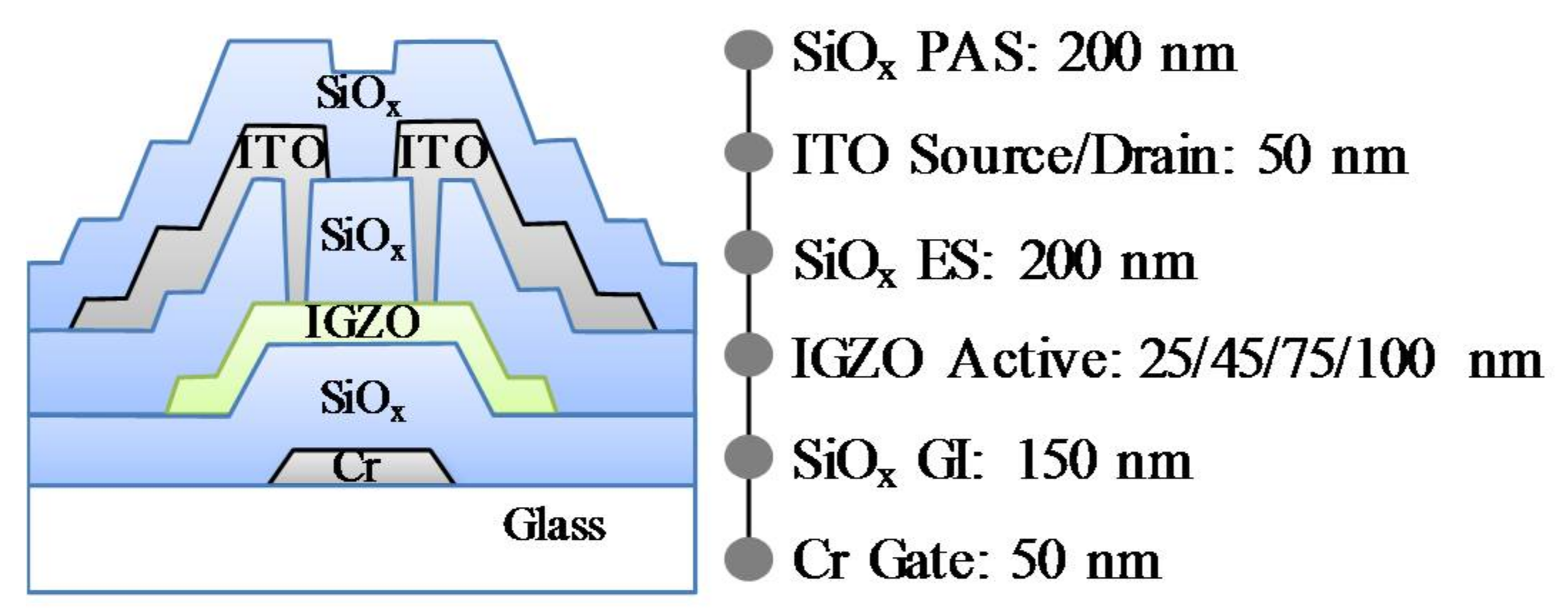
A schematic cross-sectional view and fabrication process of the bottom-gate IGZO TFT are shown in Figure 1. The fabrication procedure for the a-IGZO TFT is as follows. A chromium (Cr) gate electrode is firstly formed on a glass substrate. A SiOx gate insulator (GI) with a thickness of 150 nm is then deposited at 350 °C by plasma-enhanced chemical vapor deposition (PECVD). The a-IGZO layer with thicknesses of 25 nm, 45 nm, 75 nm, and 100 nm are deposited at 160 °C from a sintered IGZO ceramic target by direct current (DC) magnetron sputtering with a mixed gas of Ar/O2 = 29.4/0.6 sccm at a deposition pressure of 1 Pa. After patterning the IGZO film as an active channel, a SiOx film (200 nm) as an etch stopper is deposited by PECVD. Source and drain electrodes are formed using indium tin oxide (ITO) via contact holes. A 200-nm thick SiOx passivation layer is also deposited by PECVD. Finally, the IGZO TFTs are annealed in N2 ambient at 350 °C for 1 h before electrical measurements. The channel width (W) and length (L) the IGZO TFTs are 50 μm and 20 μm, respectively. All of the I–V characteristics are measured using an Agilent 4156C precision semiconductor parameter analyzer. The C–V measurements, the channel capacitance (Cgc), the gate-to-source capacitance (Cgs), and the gate-to-drain capacitance (Cgd), are measured at 1 kHz and an alternating current (AC) level of 100 mV. All of the measurements are carried out at room temperature in ambient air.
3. Results and Discussion
To investigate the thickness impact on the chemical properties and bonding states of the IGZO films, an X-ray photoelectron spectroscopy (XPS, ESCALAB250Xi, Thermo Fisher Scientific, Waltham, MA, USA) measurement is performed. Figure 2 shows the O 1s XPS spectra of the IGZO films with various thicknesses. The O 1s spectra can be resolved into three nearly Gaussian distribution peaks approximately centered at 530.7 eV, 531.4 eV, and 532.6 eV. The peaks at the binding energy of 530.7 eV (labeled as OM), 531.4 eV (labeled as OV), and 532.6 eV (labeled as OH) are attributed to the O2− ions combined with the metal atoms, oxygen deficiency, and hydroxyl groups in a stoichiometric IGZO structure, respectively [21]. The positions, areas, and area ratios of the O 1s three peaks for the IGZO films with various thicknesses are summarized in Table 1. For the 25-nm thick IGZO film, the OM/(OM + OV + OH) and OV/(OM + OV + OH) area ratios are 74.4% and 22.4%, respectively. It is suggested that the IGZO film contains a small quantity of oxygen-related defects during the short-time fabrication in the chamber. With the increase in the deposition duration, the OV/(OM + OV + OH) area ratio evidently increased, whereas the OM/(OM + OV + OH) area ratio obviously decreased. When the IGZO thickness is increased to 100 nm, the area ratios of OV/(OM + OV + OH) and OM/(OM + OV + OH) are changed remarkably to 29.1% and 67.7%, respectively. These results reveal that the long-time sputtering process deteriorates the quality of the IGZO film and accelerates the generation of the oxygen-related defects, which cause the unbalanced chemical bonds of metal and oxygen atoms. Interestingly, the area ratio of OH/(OM + OV + OH) keeps the small constant of ~3.2%, even for IGZO films fabricated under different durations, implying that the magnetron sputtering method is a promising approach to obtain a metal oxide semiconductor with small amounts of hydroxyl groups.
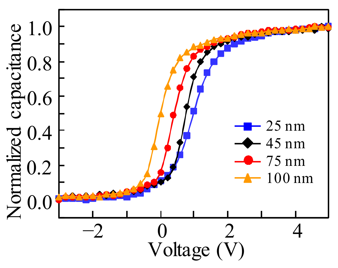
Figure 3 illustrates the C–V plot as a function of the thickness of IGZO in the ITO/IGZO/SiO2/Cr stack structure. It is noted that the increase in the IGZO thickness induces a negative shift of the flat band voltage (VFB). The variation of the VFB in the negative direction implies that the threshold voltage (Vth) of the ITO/IGZO/SiO2/Cr stack structure-based TFTs can be adjusted by using the IGZO layer with various thicknesses. In addition, the maximum negative shift of VFB is observed for the IGZO film with the thickness of 100 nm, which contributes to the largest negative shift of the Vth.
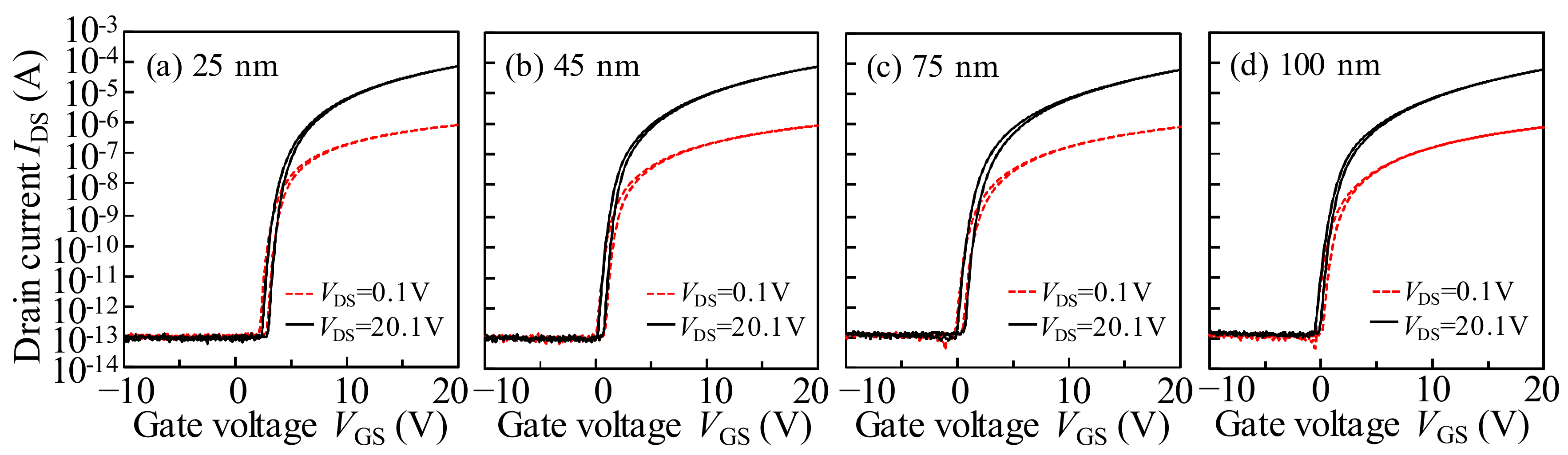
Figure 4 shows the initial transfer characteristics (IDS–VGS) of a-IGZO TFTs with various active layer thicknesses (TIGZO) measured at VDS values of 0.1 V and 20.1 V. The electrical properties, such as field effect mobility in the saturation region (μsat), Von (defined by VGS at IDS of 1 nA), subthreshold swing (SS = dVGS/dlog10(IDS)), and hysteresis of the transfer curves (defined by the difference of VGS at IDS of 1 nA between the forward and reverse sweeps) are summarized in Table 2.
The saturation mobility μsat is calculated by fitting a straight line to the plot of the square root of IDS versus VGS based on the following equation [22]:
where W and L are the channel width and length, respectively, and CSiOx is the capacitance per unit area of the GI. When the TIGZO is increased from 25 nm to 100 nm, the μsat is slightly degraded from 14.17 cm2·V−1·s−1 to 13.04 cm2·V−1·s−1. The μsat is affected by the quality of the active layer and the a-IGZO/GI interface. To confirm the influence of the TIGZO on the quality of the a-IGZO/GI interface, the hysteresis behaviors of the IGZO TFT with various TIGZO are extracted, as listed in Table 1. The identically negligible clockwise hysteresis is obtained regardless of the TIGZO, indicating that the good quality of the IGZO/GI interface is well kept during the fabrication processes for all of the IGZO TFTs. Moreover, the Von and SS values are significantly changed from 2.32 V and 323 mV/dec. in the 25-nm thick IGZO TFT to −0.33 V and 475 mV/dec. in the 100-nm thick IGZO TFT, respectively. The degraded SS value and the shifted Von in the negative VGS direction can be commonly interpreted as consequences of the total defect states and free carrier numbers being increased as the TIGZO values increased, which is consistent with previous publications [23,24] and in agreement with the C–V measurements in Figure 3. Generally, the SS value is an indicator of the maximum area density of state (Nt), including the interfacial (Dit) and the semiconductor bulk traps (Nbulk). The Nt value can be extracted from following equation [25]:
where q is the electron charge, and k is the Boltzmann constant. The Nt values were 6.53 × 10¹¹, 7.62 × 10¹¹, 8.83 × 10¹¹, and 1.03 × 1012 cm–2·eV–1 for the IGZO TFTs with the TIGZO values of 25 nm, 45 nm, 75 nm, and 100 nm, respectively. Obviously, the Nt is increased with the increase in the TIGZO value, which is consistent with the XPS results. The results exhibit that the change in the Nt mainly originated from the Nbulk, owing to the similar a-IGZO/GI interfacial quality.
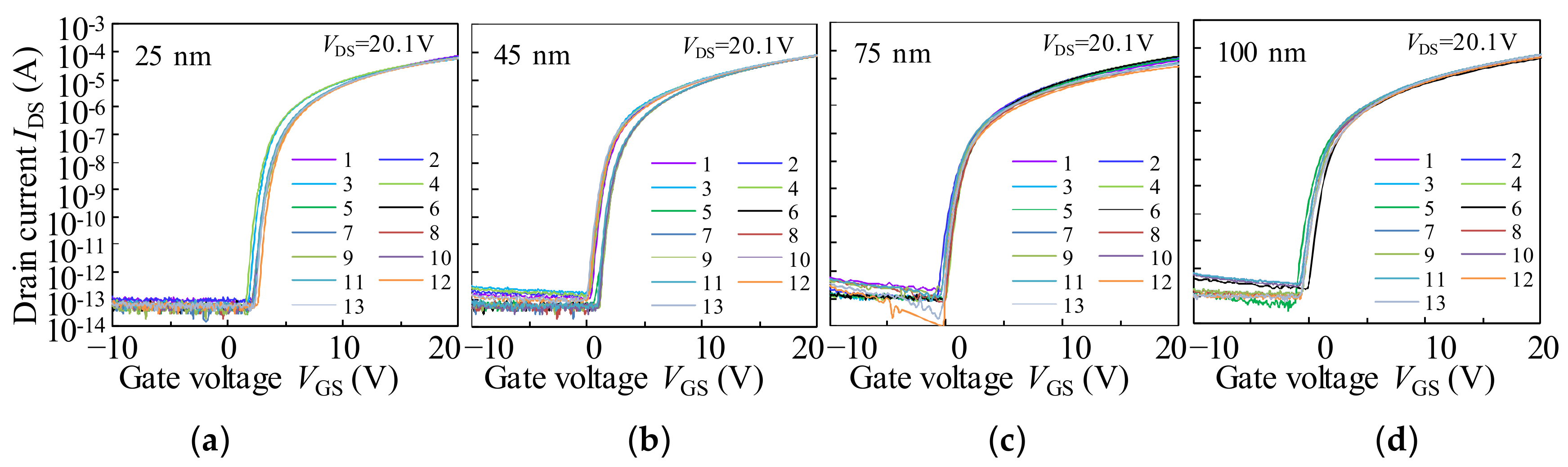
To confirm the uniformity and reproducibility of the a-IGZO TFTs with various TIGZO, the IDS–VGS curves of the 13 individual devices measured at VDS of 20.1 V are shown in Figure 5, respectively. The corresponding electrical properties, such as μsat, Von, SS, and hysteresis, are listed in Table 3. Notably, the statistical distribution of all of the parameters has the same tendency as described in Table 1 and small standard deviations, thereby indicating very good reproducibility in the fabricated a-IGZO TFTs.
To investigate the impact of the TIGZO on the stability of a-IGZO TFTs, the positive bias stress (PBS) is carried out. Figure 6a–d shows the variation in the transfer characteristics of the a-IGZO with various TIGZO under PBS with a VGS value of 20 V. The variation in Von (ΔVon) as a function of PBS duration for the a-IGZO TFTs with various TIGZO values is shown in Figure 5e. It is found that the transfer characteristics for all of the TFTs under PBS shift parallel in the positive VGS direction without SS degradation, indicating that the electrons are trapped at the interface of the a-IGZO or in the GI without introducing any defects. When the TIGZO is decreased from 100 nm to 25 nm, the ΔVon is remarkably increased from 0.52 V to 1.85 V after the stress duration of 104 s. The obtained results can be explained by the vertical electrical field distribution. Generally, the electric potential exponentially declines inside the active layer, and has a maximum transfer length called the Debye length. For the a-IGZO TFT, the calculated Debye length was ~40 nm [19]. When the TIGZO is less than Debye transfer length (TIGZO = 25 nm), the surface potential will exponentially decline into the whole active layer. Therefore, with the decrease in the TIGZO value, the electrical field will be enhanced. Under PBS, the electrons in the thinner TIGZO will be accelerated by the enhanced surface field, which are accumulated by electrical field energy and are trapped at the interface of the a-IGZO/GI or in the GI under the positive bias, leading to the large positive VGS shift. When the TIGZO increased to more than the Debye length of 40 nm, the electric field at the front-interface becomes lower, contributing to the few electrons that are trapped at the front-interface, which exhibits the small ΔVon with the increase in the TIGZO value.
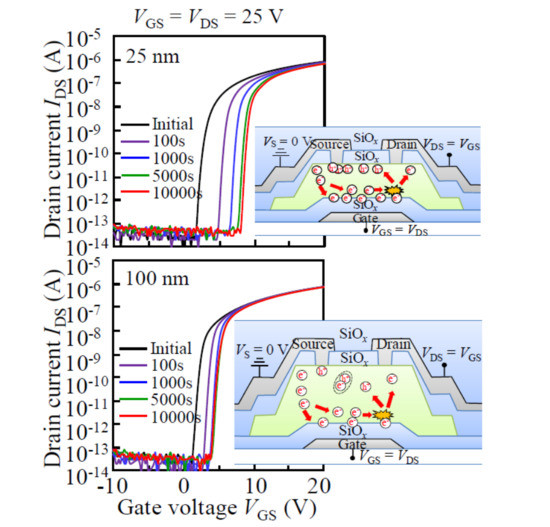
To simulate the practical operation conditions, the drain current stress (DCS) is applied to the a-IGZO TFTs with various TIGZO values. Figure 7a–d shows the variation in the transfer characteristics of the a-IGZO with various TIGZO under DCS with VGS = VDS = 25 V. The variations in ΔVon as a function of the DCS duration for the a-IGZO TFTs with various TIGZO values are shown in Figure 7e. Noticeably, the transfer curves of all of the a-IGZO TFTs exhibit a parallel shift in the positive VGS direction without SS degradation during the DCS duration. In the initial stage of DCS (<100 s), all of the transfer curves shift significantly towards the VGS direction without SS degradation. In the subsequent stage (>100 s), the amplitude of ΔVon becomes weakened, and the ΔVon increases with the decrease in the TIGZO after the DCS for 104 s.
To clarify the mechanism of the DCS-induced instability in the a-IGZO TFTs with various TIGZO, the C–V analyses of Cgc, Cgs, and Cgd before and after DCS duration of 104 s are carried out, as shown in Figure 8. Compared with the Cgc curves of the a-IGZO TFTs with various TIGZO values in the initial stage and after DCS duration, all of the Cgc curves exhibited a positive VGS shift with distortion in the off state of the C–V curves. The shift of the C–V curves is weakened as the TIGZO value increases, which has a similar tendency to the I–V curves, as shown in Figure 7. However, the shift amplitude of the C–V curves is smaller than that of the I–V curves, indicating that the less free carriers are trapped, or the trapped carriers are partly de-trapped during the C–V measurement after the DCS. Furthermore, the hump phenomenon in the off state of the C–V curves becomes weakened as the TIGZO values increase, which is hardly observed in the I–V curves. To further investigate the origin of the hump phenomenon in the off state of the C–V curves, the Cgs and Cgd values before and after the DCS are measured. Note that the both Cgs and Cgd curves exhibit a parallel shift in the positive VGS direction. However, the hump phenomenon is only observed in the Cgs curve rather than the Cgd curve during the DCS.
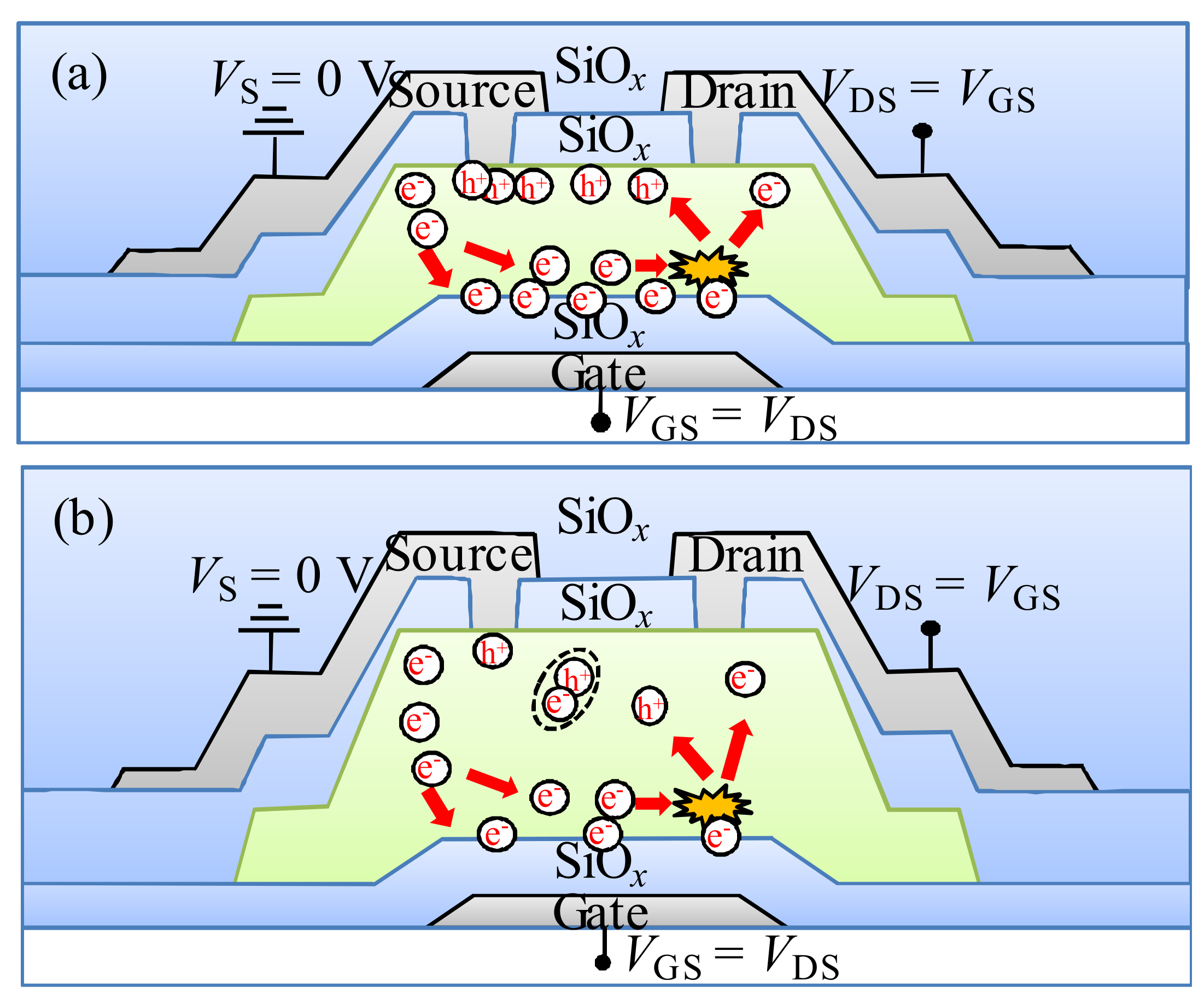
In terms of the a-IGZO TFT with a TIGZO of 25 nm under the DCS (VDS = VGS), the electrons are transported from the source to drain side along the front-channel interface, which contributes to a depletion region near the drain side. Combined with the case of 25-nm thick IGZO TFT under the PBS, in the initial stage of DCS (<100 s), the electrons are accelerated to the front-channel under the high vertical electric field. Then, they are trapped at the interface of the a-IGZO/GI or injected into the GI, resulting in a significantly positive VGS shift of the transfer curve. Simultaneously, the electrons are accelerated from the source to the drain side under the lateral electric field, resulting in the impact ionization occurring at the drain side of the channel [12]. Subsequently, the electron-hole pairs are generated by impact ionization near the drain side. The generated electrons and holes are collected at the front-channel and the etch-stopper/IGZO (back-channel) interfaces, respectively. The generated holes flow towards the source side along the back-channel interface and cause a lowered potential barrier near the source side, leading to the additional charge response in the C–V measurement, which contributes to the hump in the off state of the Cgs curve. The schematic diagram of DCS-induced degradation in the IGZO TFT with the TIGZO of 25 nm is illustrated in Figure 9a. In the subsequent stage (>100 s), with the extension of DCS duration, the more generated holes are accumulated near the source side, which contributes to the increase in the body potential. Therefore, the ΔVon of the transfer curve is weakened with the DCS duration.
When the TIGZO value is increased to 45 nm, a similar phenomenon is observed in the a-IGZO TFT under the DCS of 104 s. Due to the reduction of the vertical electric field, the amount of the trapped electrons are decreased at the interface of the channel/GI or into the GI, leading to the smaller ΔVon of the transfer curves compared with the 25-nm thick IGZO TFT, which is in agreement with the I–V and C–V results. Meanwhile, the impact ionization occurs near the drain side under the lateral electric field. The electrons are accelerated from the source to the drain side, which induces the generation of the electron-hole pair near the drain side. The generated holes drift towards the source side along the back-channel interface. Due to the amount of free electrons that increase with the increase in the TIGZO, the recombination probability of the holes and electrons are enlarged during the hole drifting. The number of the collected holes at the source side is reduced, contributing to the small hump in the off state of the Cgs curve. When the TIGZO is further increased to 75 nm or 100 nm, the positive VGS shift of the transfer curves is significantly decreased due to the weaker vertical electric field with the increase in the TIGZO value, contributing to the slightly positive VGS shift of the I–V and C–V curves. The schematic diagram of the mechanism of DCS-induced instability in the IGZO TFT with the thicker TIGZO is illustrated in Figure 9b. The generated holes induced by the impact ionization in the drain region are drifted from the drain to the source side along the back-channel under the vertical and lateral electric fields. The holes would suffer easily from the recombination with the more free electrons in the thicker IGZO layer. Therefore, the slight hump in the off state of the Cgs curve is attributed to the few holes that are accumulated at the back-channel near the source side.
Besides the TIGZO value, the architecture of devices also plays a critical role in the DCS-induced instability of the TFTs. On the basis of our previous publication [26], the role of impact ionization is strongly dependent on channel scale, and exhibits two types of dependences on channel length and width. When the DCS is applied to the TFTs with a fixed channel length and different channel widths, the stronger impact ionization can be observed for the wider channel width TFT, leading to the high heating temperature. On the other hand, when the DCS is carried out on the devices with a fixed channel width and different channel lengths, the stronger impact ionization can be obtained for the shorter channel length TFT. Therefore, besides the proper TIGZO, the a-IGZO TFTs with the relatively long length and short width may effectively minimize the impact ionization effect, improving the DCS-induced stability of the a-IGZO TFTs.
4. Conclusions
In this study, the initial electrical properties, PBS, and DCS-induced instabilities of a-IGZO TFTs with various TIGZO are investigated. As the TIGZO values increased, the Von decreased, while the SS slightly increased because the total defect states and free carrier numbers were increased as the increase in the TIGZO. It is found that the ΔVon under PBS is aggravated as the decrease in the TIGZO, which is due to the enhancement of the vertical electrical field in the channel. In addition, the DCS-induced instability in the a-IGZO TFTs with various TIGZO values is revealed by the combination of I–V and C–V measurements. The C–V results indicate that an anomalous hump phenomenon is only observed in the off state of the Cgs curve for all of the a-IGZO TFTs. This is because the impact ionization occurs near the drain side of the channel and the generated holes flow towards the source side along the back-channel interface under the lateral electric field, which causes a lowered potential barrier near the source side. Since the amount of free electrons increase with the increase in the TIGZO values, the recombination probability of the generated holes and electrons are enlarged during the hole drifting, leading to the weakened hump phenomenon as the the TIGZO values increased. This study points out that material and fabrication engineering in the drain region should be well considered, even for the high-performance oxide TFTs.
Acknowledgments
The authors acknowledge all support from the National Key Research and Development Program of China (2016YFA0202403), the National Nature Science Foundation of China (61674098, 91733301), the Natural Science Foundation of Shaanxi Provincial Department of Education (2017KW-023, 2017JM6020), the Fundamental Research Funds for the Central Universities (GK201603053, GK201603054, GK201702003, GK201601010), the Changjiang Scholar and the Innovative Research Team (IRT_14R33) and the Chinese National 1000-talent-plan program (Grant No. 111001034). The authors would like to thank Idemitsu Kosan Co. Ltd., for their support throughout this work. This work was partly supported by JSPS KAKENHI Grant Number 16K06309.
Author Contributions
M. Furuta and D. Wang conceived and designed the experiments; D. Wang, W. Zhao, and H. Li performed the experiments; D. Wang analyzed the data; D. Wang wrote the paper.
Conflicts of Interest
The authors declare no conflict of interest.
References
- Nomura, K.; Ohta, H.; Takagi, A.; Kamiya, T.; Hirano, M.; Hosono, H. Room-temperature fabrication of transparent flexible thin-film transistors using amorphous oxide semiconductors. Nature 2004, 432, 488–492. [Google Scholar] [CrossRef] [PubMed]
- Lee, S.-H.; Kim, T.; Lee, J.; Avis, C.; Jang, J. Solution-processed gadolinium doped indium-oxide thin-film transistors with oxide passivation. Appl. Phys. Lett. 2017, 110, 122102. [Google Scholar] [CrossRef]
- Martins, J.; Bahubalindruni, P.; Rovisco, A.; Kiazadeh, A.; Martins, R.; Fortunato, E.; Barquinha, P. Bias stress and temperature impact on InGaZnO TFTs and circuits. Materials 2017, 10, 680. [Google Scholar] [CrossRef] [PubMed]
- Wang, W.-H.; Lyu, S.-R.; Hredia, E.; Liu, S.-H.; Jiang, P.-H.; Liao, P.-Y.; Chang, T.-C.; Chen, H.-M. Competing weak localization and weak antilocalization in amorphous indium–gallium–zinc-oxide thin-film transistors. Appl. Phys. Lett. 2017, 110, 022106. [Google Scholar] [CrossRef]
- Zhang, J.; Yang, J.; Li, Y.; Wilson, J.; Ma, X.; Xin, Q.; Song, A. High performance complementary circuits based on p-SnO and n-IGZO thin-film transistors. Materials 2017, 10, 319. [Google Scholar] [CrossRef] [PubMed]
- Hung, M.P.; Wang, D.; Jiang, J.; Furuta, M. Negative bias and illumination stress induced electron trapping at back-channel interface of InGaZnO thin-film transistor. ECS Solid State Lett. 2014, 3, Q13–Q16. [Google Scholar] [CrossRef]
- Hirao, T.; Furuta, M.; Hiramatsu, T.; Matsuda, T.; Li, C.; Furuta, H.; Hokari, H.; Yoshida, M.; Ishii, H.; Kakegawa, M. Bottom-gate zinc oxide thin-film transistors (ZnO TFTs) for AM-LCDs. IEEE Trans. Electron Dev. 2008, 55, 3136–3142. [Google Scholar] [CrossRef]
- Kim, K.S.; Ahn, C.H.; Kang, W.J.; Cho, S.W.; Jung, S.H.; Yoon, D.H.; Cho, H.K. An all oxide-based imperceptible thin-film transistor with humidity sensing properties. Materials 2017, 10, 530. [Google Scholar] [CrossRef] [PubMed]
- Wang, D.; Hung, M.P.; Jiang, J.; Toda, T.; Furuta, M. Suppression of degradation induced by negative gate bias and illumination stress in amorphous InGaZnO thin-film transistors by applying negative drain bias. ACS Appl. Mater. Interfaces 2014, 6, 5713–5718. [Google Scholar] [CrossRef] [PubMed]
- Billah, M.M.; Jang, J. Millisecond positive bias recovery of negative bias illumination stressed amorphous InGaZnO thin-film transistors. IEEE Electron Device Lett. 2017, 38, 477–480. [Google Scholar] [CrossRef]
- Fujii, M.; Yano, H.; Hatayama, T.; Uraoka, Y.; Fuyuki, T.; Jung, J.S.; Kwon, J.Y. Thermal analysis of degradation in Ga2O3–In2O3–ZnO thin-film transistors. Jpn. J. Appl. Phys. 2008, 47, 6236–6240. [Google Scholar] [CrossRef]
- Choi, S.-H.; Han, M.-K. Effect of channel widths on negative shift of threshold voltage, including stress induced hump phenomenon in InGaZnO thin-film transistors under high-gate and drain bias stress. Appl. Phys. Lett. 2012, 100, 043503. [Google Scholar] [CrossRef]
- Valdinoci, M.; Colalongo, L.; Baccarani, G.; Fortunato, G.; Pecora, A.; Policicchio, I. Floating body effects in polysilicon thin-film transistors. IEEE Trans. Electron Dev. 1997, 44, 2234–2241. [Google Scholar] [CrossRef]
- Park, H.-W.; Park, K.; Kwon, J.-Y.; Choi, D.; Chung, K.-B. Effect of active layer thickness on device performance of tungsten-doped InZnO thin-film transistor. IEEE Trans. Electron Dev. 2016, 64, 159–163. [Google Scholar] [CrossRef]
- Park, J.; Kim, Y.S.; Kim, J.H.; Park, K.; Park, Y.C.; Kim, H.-S. The effects of active layer thickness and annealing conditions on the electrical performance of ZnON thin-film transistors. J. Alloy. Compd. 2016, 688, 666–671. [Google Scholar] [CrossRef]
- Yang, Z.; Yang, J.; Meng, T.; Qu, M.; Zhang, Q. Influence of channel layer thickness on the stability of amorphous indium zinc oxide thin film transistors. Mater. Lett. 2016, 166, 46–50. [Google Scholar] [CrossRef]
- Avis, C.; Hwang, H.R.; Jang, J. Effect of channel layer thickness on the performance of Indium–Zinc–Tin oxide thin film transistors manufactured by inkjet printing. ACS Appl. Mater. Interfaces 2014, 6, 10941–10945. [Google Scholar] [CrossRef] [PubMed]
- Jeong, J.; Hong, Y. Debye length and active layer thickness-dependent performance variations of amorphous oxide-based TFTs. IEEE Trans. Electron Dev. 2012, 59, 710–714. [Google Scholar] [CrossRef]
- Li, Y.; Pei, Y.L.; Hu, R.Q.; Chen, Z.M.; Zhao, Y.; Shen, Z.; Fan, B.F.; Liang, J.; Wang, G. Effect of channel thickness on electrical performance of amorphous IGZO thin-film transistor with atomic layer deposited alumina oxide dielectric. Curr. Appl. Phys. 2014, 14, 941–945. [Google Scholar] [CrossRef]
- Singh, T.; Lehnen, T.; Leuning, T.; Sahu, D.; Mathur, S. Thickness dependence of optoelectronic properties in ALD grown ZnO thin films. Appl. Surf. Sci. 2014, 289, 27–32. [Google Scholar] [CrossRef]
- Wang, D.; Jiang, J.; Furuta, M. Investigation of carrier generation mechanism in fluorine-doped n+ In–Ga–Zn-O for self-aligned thin-film transistors. J. Disp. Technol. 2016, 12, 258–262. [Google Scholar] [CrossRef]
- Yue, L.; Pu, H.-F.; Li, H.-L.; Pang, S.-J.; Zhang, Q. Effect of active layer thickness on device performance of a-LZTO thin-film transistors. Superlattices Microstruct. 2013, 57, 123–128. [Google Scholar] [CrossRef]
- Chen, A.H.; Cao, H.T.; Zhang, H.Z.; Liang, L.Y.; Liu, Z.M.; Yu, Z.; Wan, Q. Influence of the channel layer thickness on electrical properties of indium zinc oxide thin-film transistor. Microelectron. Eng. 2010, 87, 2019–2023. [Google Scholar] [CrossRef]
- Woo, C.H.; Kim, Y.Y.; Kong, B.H.; Cho, H.K. Effects of the thickness of the channel layer on the device performance of InGaZnO thin-film-transistors. Surf. Coat. Technol. 2010, 205, S168–S171. [Google Scholar] [CrossRef]
- Wang, Y.; Sun, X.W.; Goh, G.K.L.; Demir, H.V.; Yu, H.Y. Influence of channel layer thickness on the electrical performances of inkjet-printed In-Ga-Zn oxide thin-film transistors. IEEE Trans. Electron Dev. 2011, 58, 480–485. [Google Scholar] [CrossRef] [Green Version]
- Urakawa, S.; Tomai, S.; Ueoka, Y.; Yamazaki, H.; Kasami, M.; Yano, K.; Wang, D.; Furuta, M.; Horita, M.; Ishikawa, Y.; et al. Thermal distribution in amorphous InSnZnO thin-film transistor. Phys. Status Solidi C 2013, 10, 1561–1564. [Google Scholar] [CrossRef]
Figure 1.
A schematic cross-sectional view and fabrication process of the bottom-gate indium gallium zinc oxide (IGZO) thin-film transistor (TFT).
Figure 1.
A schematic cross-sectional view and fabrication process of the bottom-gate indium gallium zinc oxide (IGZO) thin-film transistor (TFT).

Figure 2.
X-ray photoelectron spectroscopy (XPS) spectra of O 1s peaks of the IGZO films with the thickness of (a) 25 nm; (b) 45 nm; (c) 75 nm; and (d) 100 nm, respectively.
Figure 2.
X-ray photoelectron spectroscopy (XPS) spectra of O 1s peaks of the IGZO films with the thickness of (a) 25 nm; (b) 45 nm; (c) 75 nm; and (d) 100 nm, respectively.

Figure 3.
Capacitance–voltage (C–V) characteristics of the indium tin oxide (ITO)/IGZO/SiO2/Cr stack structure with various TIGZO.
Figure 3.
Capacitance–voltage (C–V) characteristics of the indium tin oxide (ITO)/IGZO/SiO2/Cr stack structure with various TIGZO.

Figure 4.
The initial transfer characteristics (IDS–VGS) of amorphous indium gallium zinc oxide (a-IGZO) TFTs with various TIGZO of (a) 25 nm; (b) 45 nm; (c) 75 nm; and (d) 100 nm measured at VDS of 0.1 and 20.1 V, respectively.
Figure 4.
The initial transfer characteristics (IDS–VGS) of amorphous indium gallium zinc oxide (a-IGZO) TFTs with various TIGZO of (a) 25 nm; (b) 45 nm; (c) 75 nm; and (d) 100 nm measured at VDS of 0.1 and 20.1 V, respectively.

Figure 5.
The IDS–VGS of 13 individual TFTs with various TIGZO of (a) 25 nm; (b) 45 nm; (c) 75 nm; and (d) 100 nm measured at VDS of 20.1, respectively.
Figure 5.
The IDS–VGS of 13 individual TFTs with various TIGZO of (a) 25 nm; (b) 45 nm; (c) 75 nm; and (d) 100 nm measured at VDS of 20.1, respectively.

Figure 6.
Evolution of transfer characteristics in the a-IGZO TFT with the TIGZO values of (a) 25 nm; (b) 45 nm; (c) 75 nm; and (d) 100 nm as a function of the 20 V positive gate bias stress (PBS) duration for 104 s; and (e) the variation in ΔVon as a function of PBS duration for the a-IGZO TFTs with various TIGZO.

Figure 7.
Evolution of transfer characteristics in the a-IGZO TFT with the TIGZO values of (a) 25 nm; (b) 45 nm; (c) 75 nm; and (d) 100 nm as a function of the drain current stress (DCS) (VGS = VDS = 25 V) duration for 104 s, and (e) the variation in ΔVon as a function of DCS duration for the a-IGZO TFTs with various TIGZO.

Figure 8.
C–V curves of (a) Cgc; (b) Cgs; and (c) Cgd in the initial and (d) Cgc; (e) Cgs; and (f) Cgd after a DCS duration of 104 s with various TIGZO.
Figure 8.
C–V curves of (a) Cgc; (b) Cgs; and (c) Cgd in the initial and (d) Cgc; (e) Cgs; and (f) Cgd after a DCS duration of 104 s with various TIGZO.

Figure 9.
The schematic diagram of the mechanism of DCS-induced instability in the IGZO TFT with the TIGZO value of (a) 25 nm and (b) 45 nm, 75 nm, or 100 nm.
Figure 9.
The schematic diagram of the mechanism of DCS-induced instability in the IGZO TFT with the TIGZO value of (a) 25 nm and (b) 45 nm, 75 nm, or 100 nm.


Table 1.
The position, areas, and area ratios of the deconvoluted O 1s peaks for the IGZO films with various thicknesses.
Table 1.
The position, areas, and area ratios of the deconvoluted O 1s peaks for the IGZO films with various thicknesses.
| O 1s | IGZO Thickness (nm) | ||||
|---|---|---|---|---|---|
| 25 | 45 | 75 | 100 | ||
| OM | Position (eV) | 530.7 | 530.7 | 530.7 | 530.7 |
| Area | 177500 | 159500 | 158000 | 156000 | |
| OV | Position (eV) | 531.4 | 531.4 | 531.4 | 531.4 |
| Area | 53500 | 55500 | 61000 | 67000 | |
| OH | Position (eV) | 532.6 | 532.6 | 532.6 | 532.6 |
| Area | 7500 | 7000 | 7000 | 7500 | |
| OM/(OM + OV + OH) area ratio (%) | 74.4 | 71.8 | 69.9 | 67.7 | |
| OV/(OM + OV + OH) area ratio (%) | 22.4 | 25.0 | 27.0 | 29.1 | |
| OH/(OM + OV + OH) area ratio (%) | 3.2 | 3.2 | 3.1 | 3.2 | |
Table 2.
The electrical properties of a-IGZO TFTs with various TIGZO.
| Thickness (nm) | 25 | 45 | 75 | 100 |
|---|---|---|---|---|
| μsat (cm2∙V−1∙s−1) | 14.17 | 14.01 | 13.62 | 13.04 |
| Von at IDS = 1 nA (V) | 2.32 | 0.27 | 0.04 | −0.33 |
| Hysteresis ΔVH (V) | 0.52 | 0.54 | 0.55 | 0.43 |
| Subthreshold swing (mV/dec.) | 323 | 367 | 416 | 475 |
Table 3.
The statistical deviation of the electrical properties of a-IGZO TFTs with various TIGZO.
| Thickness (nm) | 25 | 45 | 75 | 100 |
|---|---|---|---|---|
| μsat (cm2∙V−1∙s−1) | 13.91 ± 0.92 | 13.70 ± 0.39 | 12.50 ± 1.01 | 11.88 ± 0.34 |
| Von at IDS = 1 nA (V) | 2.29 ± 0.28 | 1.60 ± 0.46 | 1.31 ± 0.44 | 0.88 ± 0.46 |
| Hysteresis ΔVH (V) | 0.37 ± 0.18 | 0.33 ± 0.07 | 0.38 ± 0.27 | 0.28 ± 0.12 |
| SS (mV/dec.) | 279 ± 24 | 287 ± 19 | 314 ± 23 | 351 ± 26 |
© 2018 by the authors. Licensee MDPI, Basel, Switzerland. This article is an open access article distributed under the terms and conditions of the Creative Commons Attribution (CC BY) license (http://creativecommons.org/licenses/by/4.0/).
Share and Cite
MDPI and ACS Style
Wang, D.; Zhao, W.; Li, H.; Furuta, M. Drain Current Stress-Induced Instability in Amorphous InGaZnO Thin-Film Transistors with Different Active Layer Thicknesses. Materials 2018, 11, 559. https://doi.org/10.3390/ma11040559
AMA Style
Wang D, Zhao W, Li H, Furuta M. Drain Current Stress-Induced Instability in Amorphous InGaZnO Thin-Film Transistors with Different Active Layer Thicknesses. Materials. 2018; 11(4):559. https://doi.org/10.3390/ma11040559
Chicago/Turabian StyleWang, Dapeng, Wenjing Zhao, Hua Li, and Mamoru Furuta. 2018. "Drain Current Stress-Induced Instability in Amorphous InGaZnO Thin-Film Transistors with Different Active Layer Thicknesses" Materials 11, no. 4: 559. https://doi.org/10.3390/ma11040559
Note that from the first issue of 2016, this journal uses article numbers instead of page numbers. See further details here.