Review

A Review of Power Electronic Devices for Heavy Goods Vehicles Electrification: Performance and Reliability

1
School of Engineering, University of Warwick, Coventry CV4 7AL, UK
2
Faculty of Engineering, University of Bristol, Bristol BS8 1QU, UK
3
Engineering and Mathematics Department, Sheffield Hallam University, Sheffield S1 1WB, UK
*
Author to whom correspondence should be addressed.
Energies 2023, 16(11), 4380; https://doi.org/10.3390/en16114380
Submission received: 30 April 2023 / Revised: 18 May 2023 / Accepted: 23 May 2023 / Published: 28 May 2023
(This article belongs to the Section F3: Power Electronics)

Abstract

:
This review explores the performance and reliability of power semiconductor devices required to enable the electrification of heavy goods vehicles (HGVs). HGV electrification can be implemented using (i) batteries charged with ultra-rapid DC charging (350 kW and above); (ii) road electrification with overhead catenaries supplying power through a pantograph to the HGV powertrain; (iii) hydrogen supplying power to the powertrain through a fuel cell; (iv) any combination of the first three technologies. At the heart of the HGV powertrain is the power converter implemented through power semiconductor devices. Given that the HGV powertrain is rated typically between 500 kW and 1 MW, power devices with voltage ratings between 650 V and 1200 V are required for the off-board/on-board charger’s rectifier and DC-DC converter as well as the powertrain DC-AC traction inverter. The power devices available for HGV electrification at 650 V and 1.2 kV levels are SiC planar MOSFETs, SiC Trench MOSFETs, silicon super-junction MOSFETs, SiC Cascode JFETs, GaN HEMTs, GaN Cascode HEMTs and silicon IGBTs. The MOSFETs can be implemented with anti-parallel SiC Schottky diodes or can rely on their body diodes for third quadrant operation. This review examines the various power semiconductor technologies in terms of losses, electrothermal ruggedness under short circuits, avalanche ruggedness, body diode and conduction performance.

1. Introduction

As of 2019, according to the national grid UK, long haul transportation with Heavy Goods Vehicles (HGVs) contributed 16% of the total greenhouse gas emissions due to transportation [1]. If the UK is to meet its net zero targets, the electrification of HGVs cannot be avoided. The electrification of HGVs remains one of the more challenging objectives in the decarbonisation of road transportation. This is because the power levels (500 kW and above) and range (hundreds of miles) typical of HGVs requires significantly large batteries with long charging times. Be that as it may, there is progress in the development of battery-powered HGVs. For example, Volvo recently commercialised an electric truck, called the Volvo FM Electric, with a powertrain of up to 490 kW and range of 380 km. The truck is powered by a battery pack with a capacity as high as 540 kWh, which, assuming a gravimetric energy density (of Lithium Ion Batteries) equal to 0.25 kWh/kg [2], translates into a battery mass of approximately 2.1 tonnes. This is 5% of the gross-vehicle-weight. For comparison, 415 litres of diesel have a mass of 357 kg (0.8% of the gross vehicle weight) while providing a range of over 1000 km, assuming 8 miles per gallon [3]. More importantly, unlike the current fossil fuel-powered HGVs where the mass of the fuel is reduced as it is consumed over the journey, the mass of the battery is independent of the state-of-charge. This is no longer a problem in passenger electric vehicles where battery packs ranging between 50 kWh and 100 kWh are commercially available with good mileage on a full charge (between 300 and 500 miles depending on specific driving conditions).
Electric buses are also becoming mainstream [4,5,6]. Eighty seat capacity electric buses with 250 kW powertrains and over 660 kWh battery capacity have been commercialised with a gross weight of 27.6 tonnes and proclaimed mileage of up to 250 miles. However, when it comes to HGVs with gross weights of above 30 tonnes (up to 44 tonnes) that are required to cover long haul distances, electrification is significantly more challenging in spite of the advances made by companies such as Volvo. Some studies have demonstrated that battery capacities ranging from 150 kWh (for 12 tonne vehicles) to 800 kWh (for heavier vehicles) are required for HGV electrification [7]. Various powertrain technologies for reducing the carbon footprint of the HGV industry have been explored. These include hybrid electric powertrains that combine traction power from internal combustion engines with battery-powered electric motors with and without a plug-in charging capability [8]. Other options for HGV electrification include fuel cell HGVs powered by hydrogen [9,10] or overhead catenaries powering HGVs through pantographs, called the Electric Road System (ERS) [11,12]. The advantage of the hybrid HGV is its avoidance of the battery requirement problem; however, the disadvantage is that it is not fully decarbonised since there is still an internal combustion engine. The advantage of the ERS is its avoidance of the battery and charging problem together with the fact that it operates without any carbon emissions.
Power electronics is a critical factor in HGV electrification. It enables the energy interchange between the electrical power system and the HGV battery as well as managing and controlling the flow of electrical power between the HGV battery and the traction motors. Whether HGVs are powered by batteries, overhead catenaries or hydrogen, the power electronics required for implementing the drivetrain traction converter remains the same. If the HGV is battery powered, then ultra-fast DC chargers (above 100 kW charging power) are required for charging within reasonable timeframes [13,14,15]. The larger power levels in the powertrain means that either the voltage capacity, current capacity or both will have to be increased. This has significant implications for the choice of power semiconductor devices used. Battery chargers comprise rectifiers, (which are AC/DC converters for converting three-phase AC mains power to DC power) and DC/DC converters for interfacing with the HGV battery. Traction converters are bi-directional DC/AC converters usually implemented as three-phase two-level voltage source converters with six switching units comprised of transistors and anti-parallel diodes. During forward traction, power flows from the DC battery to the AC motor via the transistors and during regenerative braking, power flows back to the battery from the motor through the diodes. Lower-rated power electronic DC/DC converters are also required to interface the high voltage battery with low voltage electrical loads in the vehicle. Figure 1 shows a schematic figure illustrating the various power flows and the converters that enable them.
Given the power ratings mentioned previously, devices with voltage ratings between 650 V and 1.2 kV are typical for EV power electronics. The most critical qualities these power devices must meet for HGV electrification are loss performance and reliability. Efficiency is important for maximizing the EV mileage, while reliability is important for safe operation. Depending on the voltage ratings, these devices can be silicon super-junction MOSFETs, silicon IGBTs, SiC Planar or Trench MOSFETs, SiC Cascode JFETs, enhancement mode GaN HEMTs or GaN Cascode HEMTs. These devices have different advantages and drawbacks as far as reliability and performance is concerned. The goal of this paper is to review the latest generation power semiconductor devices and their suitability for HGV electrification applications, as well as loss performance and reliability. Section 2 of the paper introduces the different power converters and devices used in electric HGV charging and traction applications. Section 3 assesses the measured switching losses of the different devices (except for the GaN devices), reliability and robustness performance (including short circuit, avalanche ruggedness, gate oxide robustness, body diode performance and conduction). Section 4 concludes the paper.

2. Power Converters and Devices
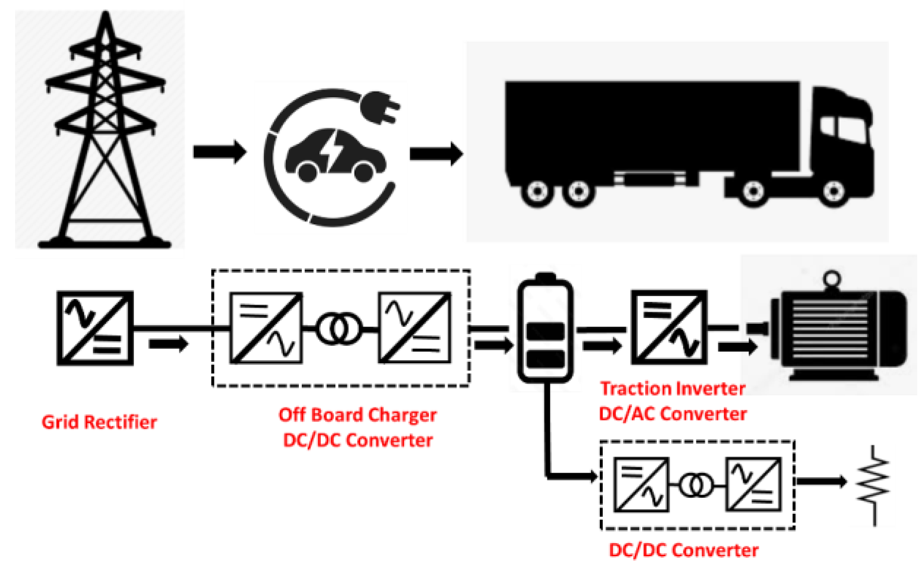
The main power electronic systems in electric HGVs are the onboard/off-board chargers and the traction converter. Other than batteries, this is where the main engineering challenges are regarding HGV electrification. In this section, the main common converter topologies for EV charging and power traction inverters are reviewed, providing an overview of the device technologies required for implementing these converters.

2.1. EV Charging

EV charging can be categorised into level 1 chargers (around 3 kW single phase AC), level 2 chargers (between 7 kW single phase AC and 22 kW 3-phase AC) and level 3 (50 kW DC and above). Level 3 charging standards include CHAdeMO (pioneered by Japan and common in Asia) and CCS (pioneered in Europe and the US). Due to the large battery sizes involved with electric HGVs, only high-power DC charging options are realistic. Assuming a 600 kWh battery, a 350 kW rapid DC charger will require more than 1 h for full charging. HGV charging stations of 350 kW charging power and above can be connected either to the low voltage distribution network (400 V) or the medium voltage distribution network (11 kV or 33 kV). There are advantages and disadvantages regarding the power electronics associated with both approaches.

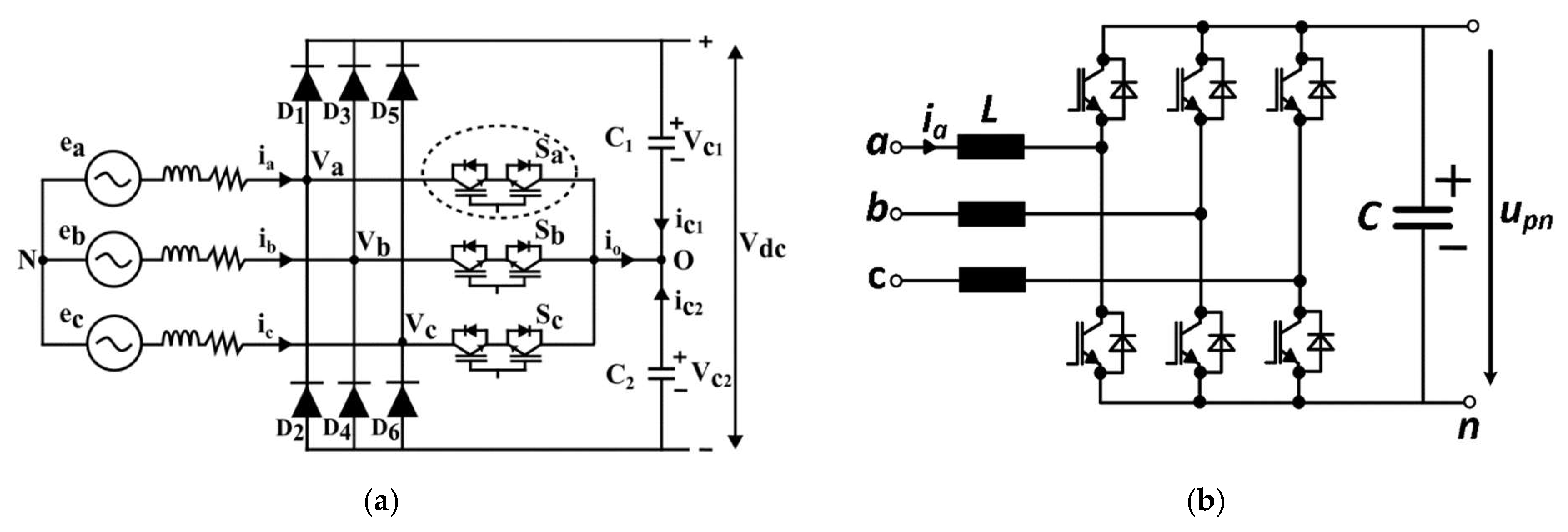
2.1.1. High Power Charging from the 400 V Network

The primary advantage with connecting to the 400 V AC system is that low-voltage-rated power devices can be used with more established and conventional converter topologies. The charger comprises of a rectifier followed by a DC/DC converter. The two popular rectifier topologies, shown below in Figure 2a,b, are the Vienna rectifier [16,17,18,19] and the active front-end rectifier [20,21,22,23]. Both rectifiers are capable of power factor correction. Connected to the 400 V ac mains, the diodes (D1 to D6) in the front end of the Vienna rectifier should be rated at 1.2 kV. With switching frequencies as high as 50 kHz, these can only be SiC Schottky Barrier Diodes (SBDs) for an acceptable switching loss performance. The transistors in the Vienna rectifier should be rated at 650 V. In the case of the AFE rectifier in Figure 2b, the power devices should be rated at 1.2 kV since the devices are blocking the entire DC link voltage, unlike in the Vienna rectifier, where they are blocking half the DC link. The primary disadvantage with charging from the 11 kV network is the additional thermal loading on the 400 V distribution transformers. Reinforcing these transformers in dense urban networks will be costly and highly disruptive, especially since they are already servicing domestic and commercial/industrial load centres.

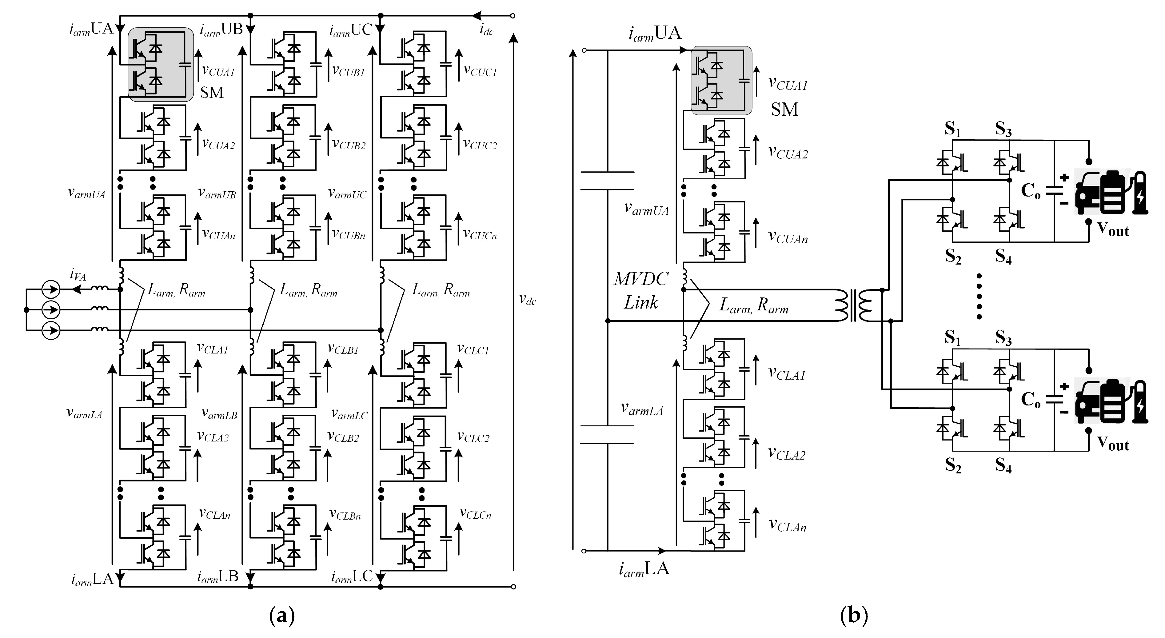
2.1.2. High Power Charging from 11 kV or 33 kV Network

The primary advantage in charging from the 11 kV and 33 kV network is that the low voltage 11 kV/400 V distribution transformers can be avoided. These transformers are numerous and are usually located in dense urban environments where upgrading will be difficult. Furthermore, incorporating EV charging with a medium voltage DC transmission (MVDC) allows other advantages for the AC system if different AC nodes in the sub-transmission and distribution network are interconnected [24,25,26,27,28]. These advantages include more flexible and reconfigurable AC power flow systems and additional resilience to faults since active and reactive power flow can be enabled between different AC distribution systems if power electronic converters are implemented and controlled. In this case, the EV charger system can be integrated with MVDC transmission and soft-open-points. The main disadvantage of charging from 11 kV or 33 kV networks is the complexity and cost of the power electronic converter, which must be designed to handle such high voltages. Due to the high voltages, either multi-level converter topologies and/or series connected devices must be used for the EV charger [29,30,31,32]. These multilevel converters include cascaded H-bridge or multi-level NPC converters, possibly with series connected devices for each level, depending on the number of levels. Figure 3a shows an MMC rectifier connected to a 3-phase AC system, while Figure 3b shows an MMC-based DC/DC converter connecting an MVDC infeed to parallel connected EV batteries. In the MMCs shown in Figure 3, the voltage rating of the power devices used will depend on the number of levels in the converter. The higher the number of levels, the lower the required voltage blocking capability of the power device and vice versa. For example, assuming the MMC is connected to a 33 kV AC system and the MVDC transmission voltage is 54 kV DC, then using 1.7 kV rated SiC MOSFETs will require 57 levels, assuming 56.72% of the voltage rating of the device is used. If the voltage rating of the device is increased to 3.3 kV, then the number of submodules required to implement the MMC reduces to 29 (also assuming 58.44% of the voltage rating is used).
High-voltage-rated devices (above 2.5 kV) are limited to silicon bipolar transistors (Thyristors and IGBTs) and SiC MOSFETs [33]. Since most Thyristors only have turn-on capability and need to be turned off by the voltage commutation of the AC system (except GTOs and IGCTs), they are not suitable for EV charging applications. IGBTs with ratings as high as 4.5 kV and 6.5 kV are commercially available; however, they usually have long tail currents and long gate delays, which makes them inapplicable for EV chargers where a high switching frequency is required for compact design. Silicon IGBTs are typically used in high voltage direct current voltage source converter (HVDC VSC) systems where offshore wind power is transmitted onshore. The switching frequencies used in such systems are significantly smaller (hundreds of Hz); hence, the switching losses are not a critical design factor. In MVDC VSC systems for EV charging stations, considerably higher switching frequencies (several kHz) will be used, hence, the switching losses means that only SiC MOSFETs’ technologies are applicable in such systems.

2.2. Traction Inverters

Based on existing diesel engine specifications currently used in Internal Combustion Engine (ICE)-powered HGVs, the powertrain of electric HGVs can require as high as 500 kW of electrical power. For an EV powertrain with a 400 V DC bus, this will mean an approximately 1.2 kA DC current and a peak AC current of 1 kA into the motor stator windings per phase. For a DC bus voltage of 800 V, the DC bus current will be 600 A, while the peak AC current will be approximately 500 A per phase. Powertrains with DC bus voltages of 400 V will require the traction converter to be implemented using 650 V rated power devices, while powertrains with 800 V DC buses will require 1.2 kV power devices. There is consensus that moving EV powertrains from 400 V DC bus voltage to 800 V DC bus voltage is beneficial for reducing losses and increasing battery charging times [34,35,36]. For both voltage classes, paralleling of multiple devices will be required for enabling large current capability. However, more devices will be required for the lower DC bus voltage. The switching frequencies used in such converters will be between 5 and 20 kHz. While 650 V and 1.2 kV silicon IGBTs have historically been used to implement EV traction inverters, SiC MOSFETs are increasingly gaining popularity for such applications [37,38,39,40,41,42,43]. At the 1.2 kV voltage level, SiC MOSFETs have a considerably reduced switching loss compared to the silicon IGBT. Likewise, SiC Schottky Barrier diodes will have significantly reduced switching losses compared to silicon PiN diodes [44]. In terms of cost and reliability, silicon IGBTs still outperform SiC MOSFETs. Hence, there is a trade-off between the switching efficiency on one hand and cost/reliability on another.

3. Performance and Reliability Assessment

In this section, some of the latest generation SiC MOSFETs and silicon devices have been tested. Experimental measurements are performed on commercially available 650 V and 1.2 kV SiC MOSFETs and IGBTs from different manufacturers. Devices rated at 1.2 kV have been selected assuming a DC link voltage of 800 V corresponding to the battery voltage, whereas 650 V rated devices are selected assuming a DC link voltage/battery voltage of 400 V. The 650 V devices can also be used in the Vienna rectifier connected to the 400 V three-phase mains. The tests performed assess the performance and reliability of the devices in hard switched applications. The loss performance can be assessed using conduction and switching measurements of the transistors and body diodes, while the reliability/robustness performance can be assessed using short circuit tests, gate oxide tests, avalanche ruggedness, etc. A fair comparison between devices under identical conditions can enable systems engineers to identify the trade-offs involved in device selection.

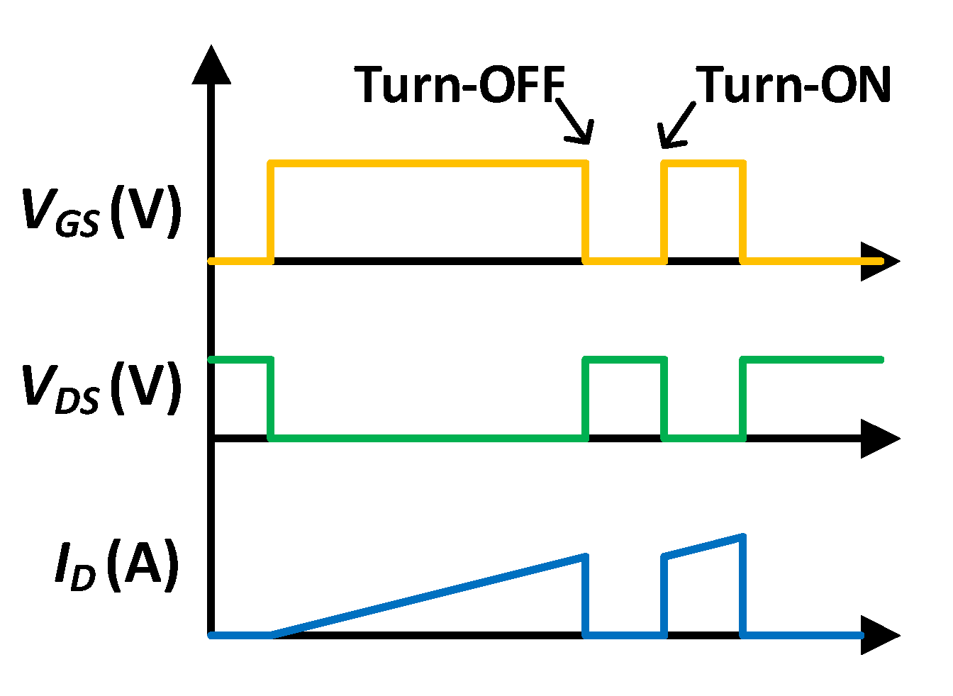
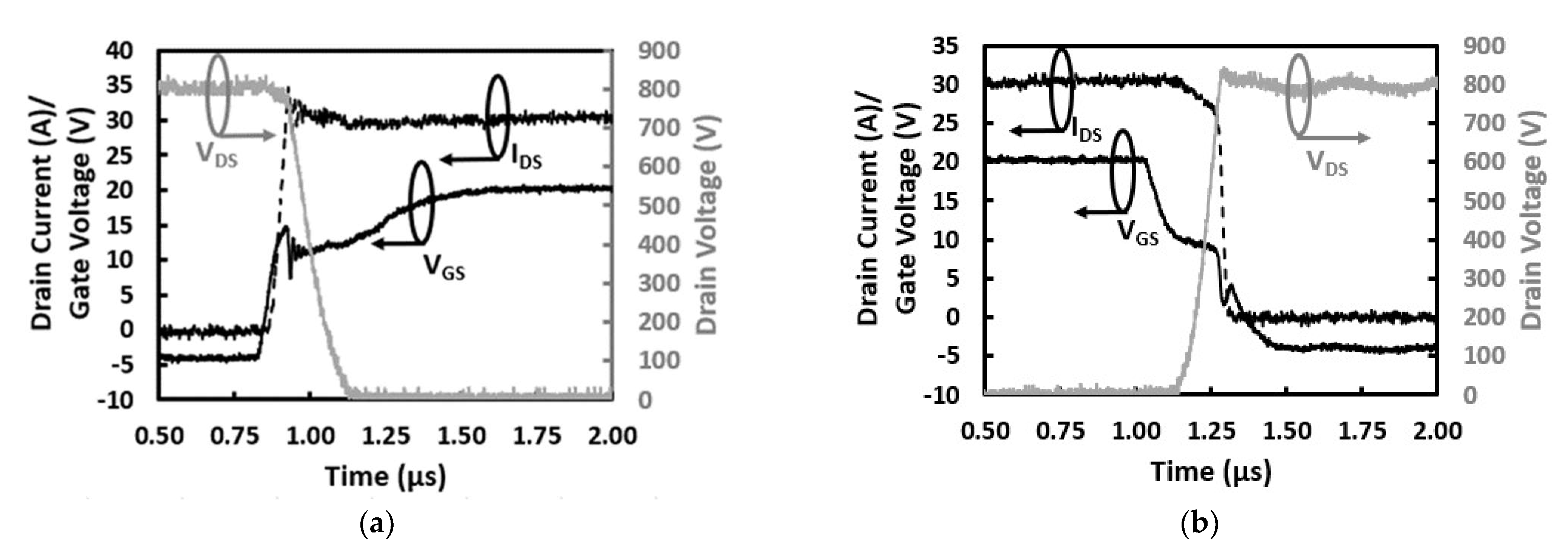
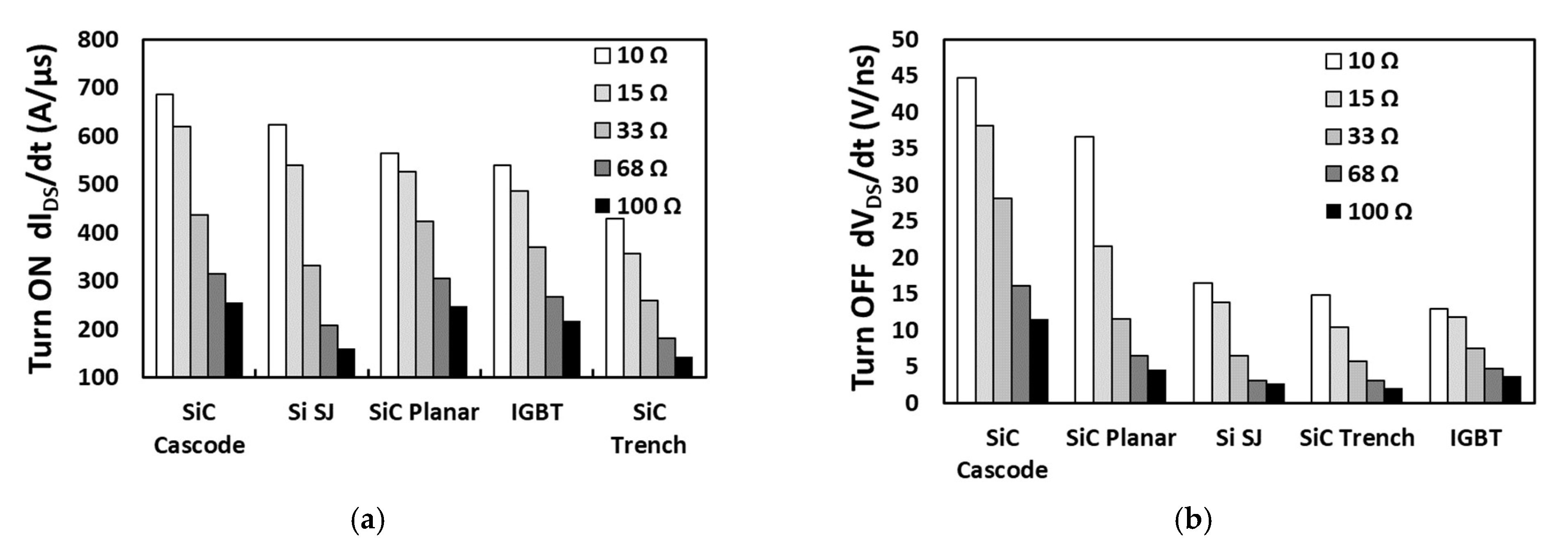
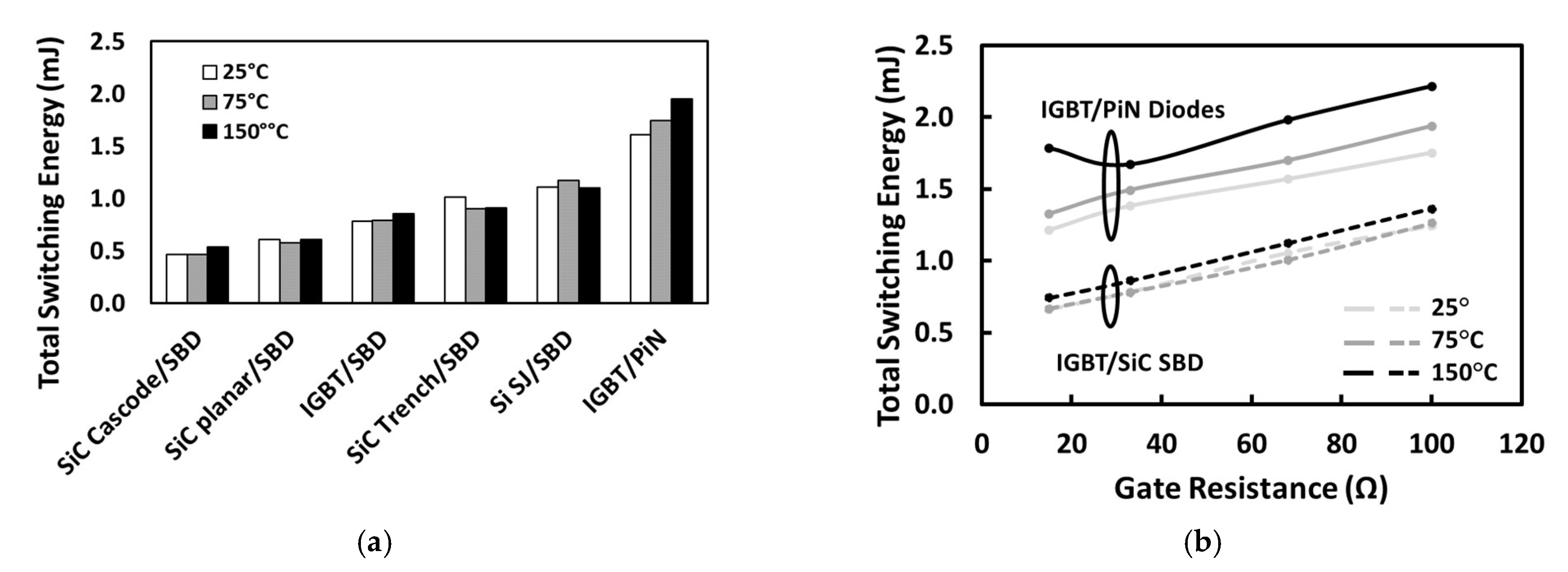
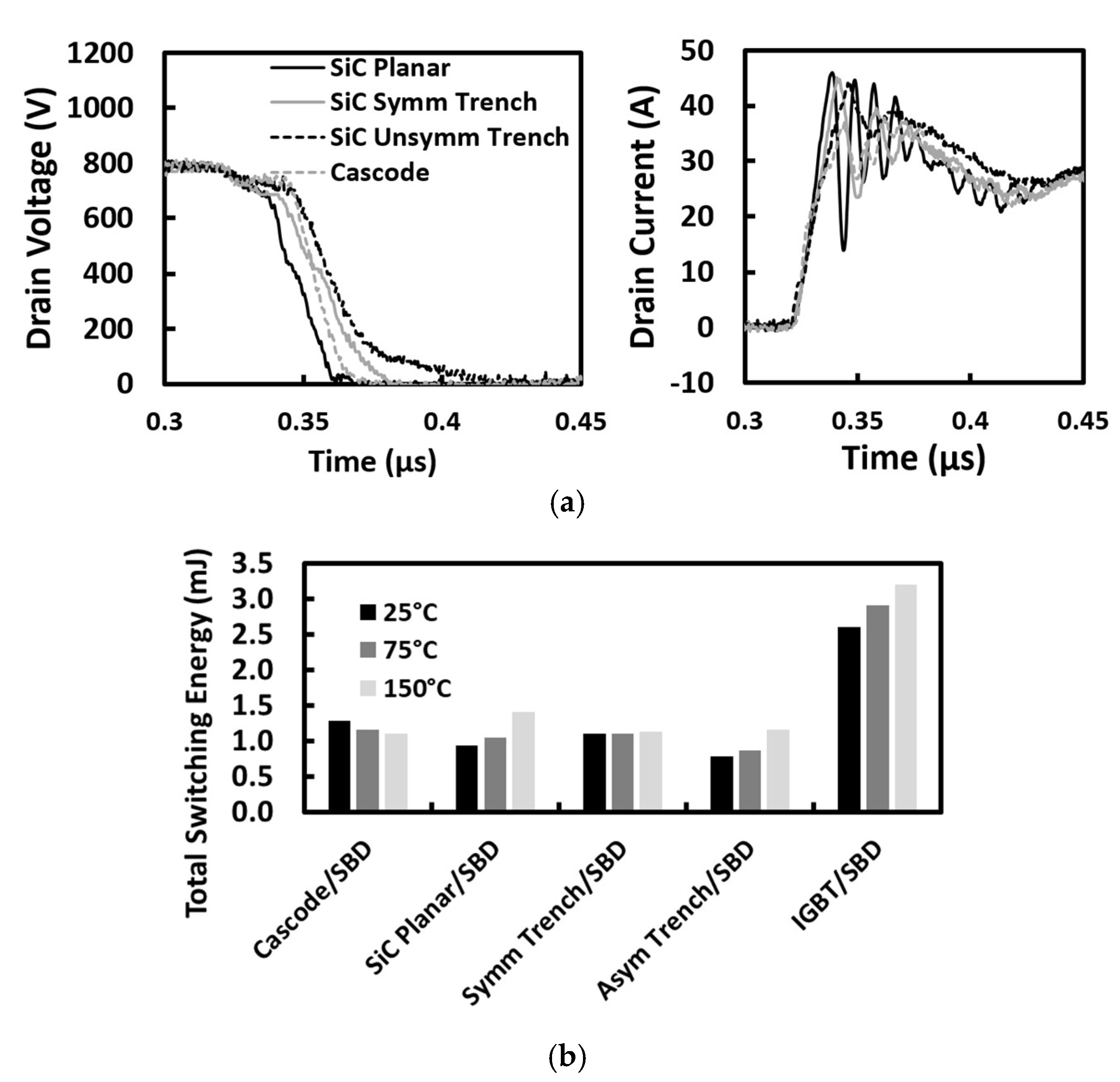
3.1. Switching Performance

The switching energy of a power transistor is measured using a double pulse set-up [45]. The double pulse experimental set up is shown in Figure 4a, while Figure 4b shows the equivalent circuit where the device under the test transistor (DUT) is identified as Q1 and the freewheeling diode is identified as D1. The other elements of the circuit are a load inductor L, DC-link capacitor CDC connected to a DC power supply of voltage VDC and a gate driving circuit with a supply voltage VGG, which is used for turning the transistor ON/OFF using an external gate resistance RGEXT. This type of test circuit usually allows one to adjust the temperature of the DUT, allowing dynamic characterisation at different temperatures. It is also common to drive the transistor using a positive gate voltage VGG for turning on the device and a negative gate voltage VEE for turning off the device. This helps with the issue of parasitic turn-on [46,47].
The circuit works by first adjusting the power supply/DC link capacitor to the test voltage, which should be the DC bus voltage of the HGV. The DC link provides the current during the test and allows the use of a power supply with a lower current rating than the load current being tested [45]. As the DUT transistor turns on (first pulse), the inductor (L) is charged. The duration of the ON time tON is determined by the target load current of the switching energy test Itest, according to Equation (1).
I t e s t = V D C t O N L
As the DUT is turned off, the current commutates to the diode at a rate that depends on the turn-off switching speed of the DUT (controlled by the external gate resistance RGEXT). The turn-off energy ESW-OFF of the transistor is measured here. The DUT transistor is subsequently switched on for a second time and the turn-on switching energy ESW-ON is measured for that switching transient. The switching energies are calculated using Equation (2), where tSW is the switching time (which can be the turn-on switching time or turn-off switching time).
E S W = 0 t S W I D S V D S   d t
An idealised double pulse test sequence is shown in Figure 5, whereas an experimental example of the turn-on and turn-off current and voltage waveforms for a 1200 V SiC Planar MOSFET are shown in Figure 6a,b. The measurements were performed using a DC link voltage of 800 V, load current of 30 A, junction temperature of 25 °C, a low side external gate resistance of 68 Ω and a gate driver with voltages of +20 V and −5 V for turning the transistor on and off, respectively.
The DPT configuration is paramount for evaluating the switching performance of devices, and there are different commercial tests setups and support equipment available from different manufacturers [49,50,51] indicating the relevance of these types of measurements.
An investigation on the switching performance of different 650 V and 900 V device technologies was performed in [52]. The devices include SiC planar MOSFETs, SiC trench MOSFETs, SiC cascode JFETs, Si super-junction MOSFETs and Si IGBTs. These devices are suitable for 400 V DC link voltages and Figure 7a,b shows the turn-on dI/dt and turn-off dV/dt at different gate resistances for a load current of 20 A and a DC link voltage of 400 V. Figure 8a shows the measured switching energies of all the 650 V/900 V rated technologies switched with a 400 V DC link and 20 A load current, using a SiC Schottky barrier diode as the freewheeling diode. In summary, the SiC Cascode JFETs and SiC Planar MOSFET were the best performing devices with the lowest switching losses and highest switching rates (dV/dt and dI/dt).
Switching characterisation of 650 V devices using a DPT configuration was also performed in [43] with a focus on automotive traction applications. A summary of the results is shown in Figure 8. In Figure 8a, the IGBT is switched with a PiN diode and a SiC SBD as freewheeling diodes to highlight the importance of the SiC SBD and how it affects the transistor switching energy. Figure 8b compares the switching energy measurements of the silicon IGBT with a freewheeling PiN diode with the same IGBT, as well as with a freewheeling Schottky diode as a function of the gate resistance at different temperatures. From Figure 8b, it is apparent that using the PiN diode increases the transistor losses compared to the SiC SBD.
For DC link voltages of 800 V, the devices selected are 1.2 kV rated. Clamped inductive switching measurements have been performed on 1.2 kV SiC MOSFETs and latest generation fast silicon IGBTs. The SiC MOSFETs were a 1.2 kV SiC Planar MOSFET from Wolfspeed with datasheet reference C2M0080120D, 1.2 kV SiC Symmetrical Trench MOSFET from ROHM with datasheet reference SCT3080KLHRC11, 1.2 kV Asymmetrical Trench MOSFET from Infineon with datasheet reference AIMW120R080M1, a 1.2 kV SiC Cascode JFET from United SiC Technologies with datasheet reference UJ3C120080K3S and a silicon IGBT from Infineon with datasheet reference IKW15N120CS7. The IGBT used is a comparatively fast IGBT optimised for hard switching. All devices are of a similar current rating and were switched using a Schottky barrier diode as a freewheeling diode. The turn-on current and voltage waveforms for all the SiC devices are demonstrated in Figure 9a, while the total measured switching energy for all devices are shown in Figure 9b at three different junction temperatures (25 °C, 75 °C and 150 °C) while switching 30 A. The results in Figure 9 demonstrate that the SiC devices have a similar switching performance, which has approximately 50% lower switching energy than the silicon IGBT. These results highlight that while silicon IGBTs may be able to compete with SiC MOSFETs at 650 V in terms of switching energy, at 1.2 kV, their switching energies become significantly higher.

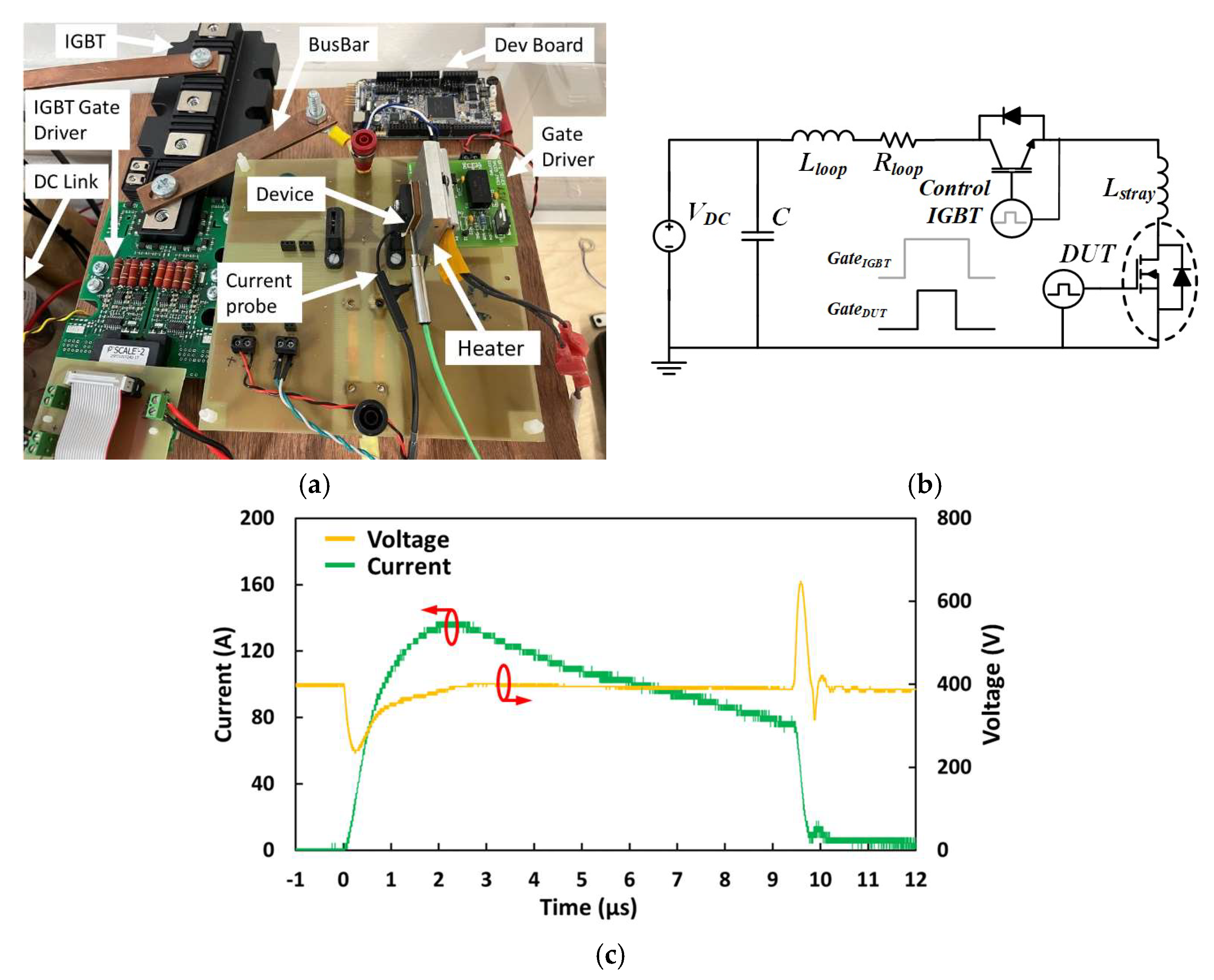
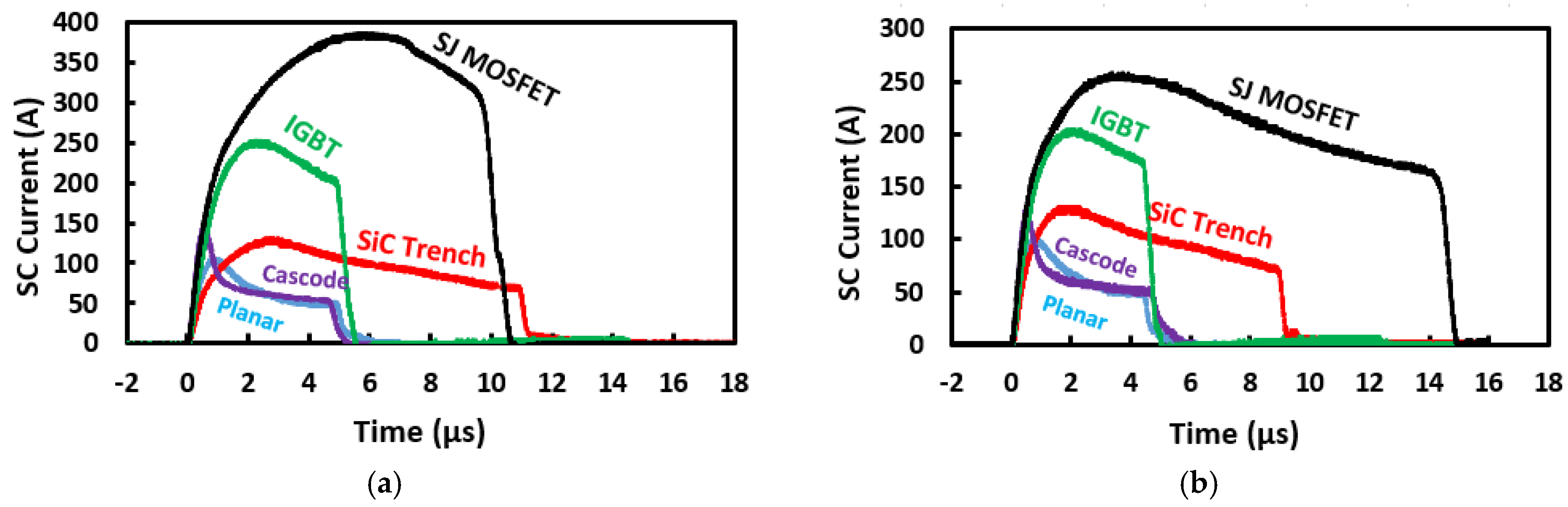
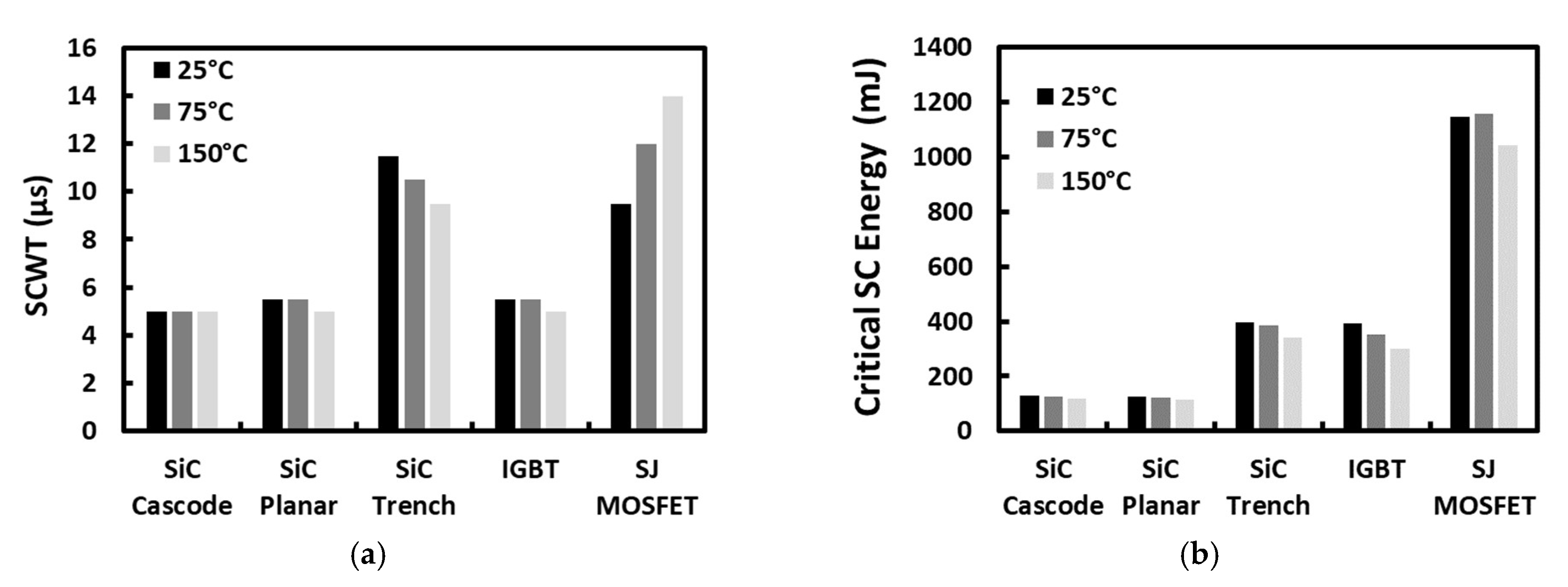
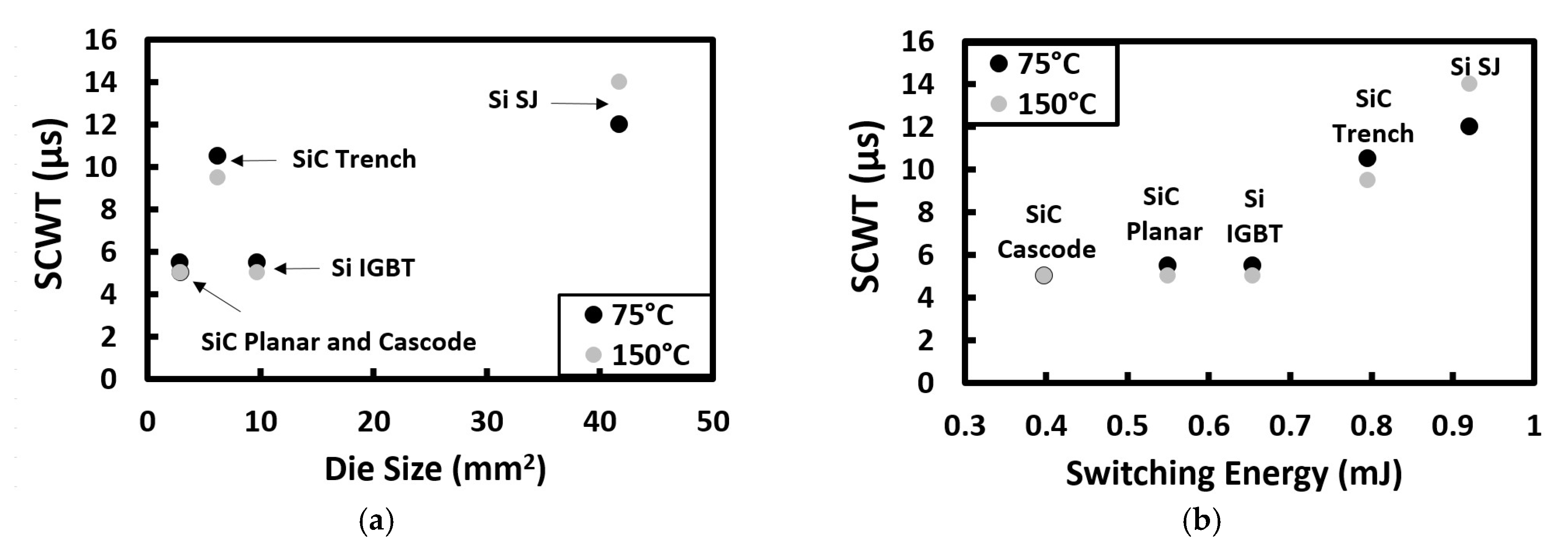
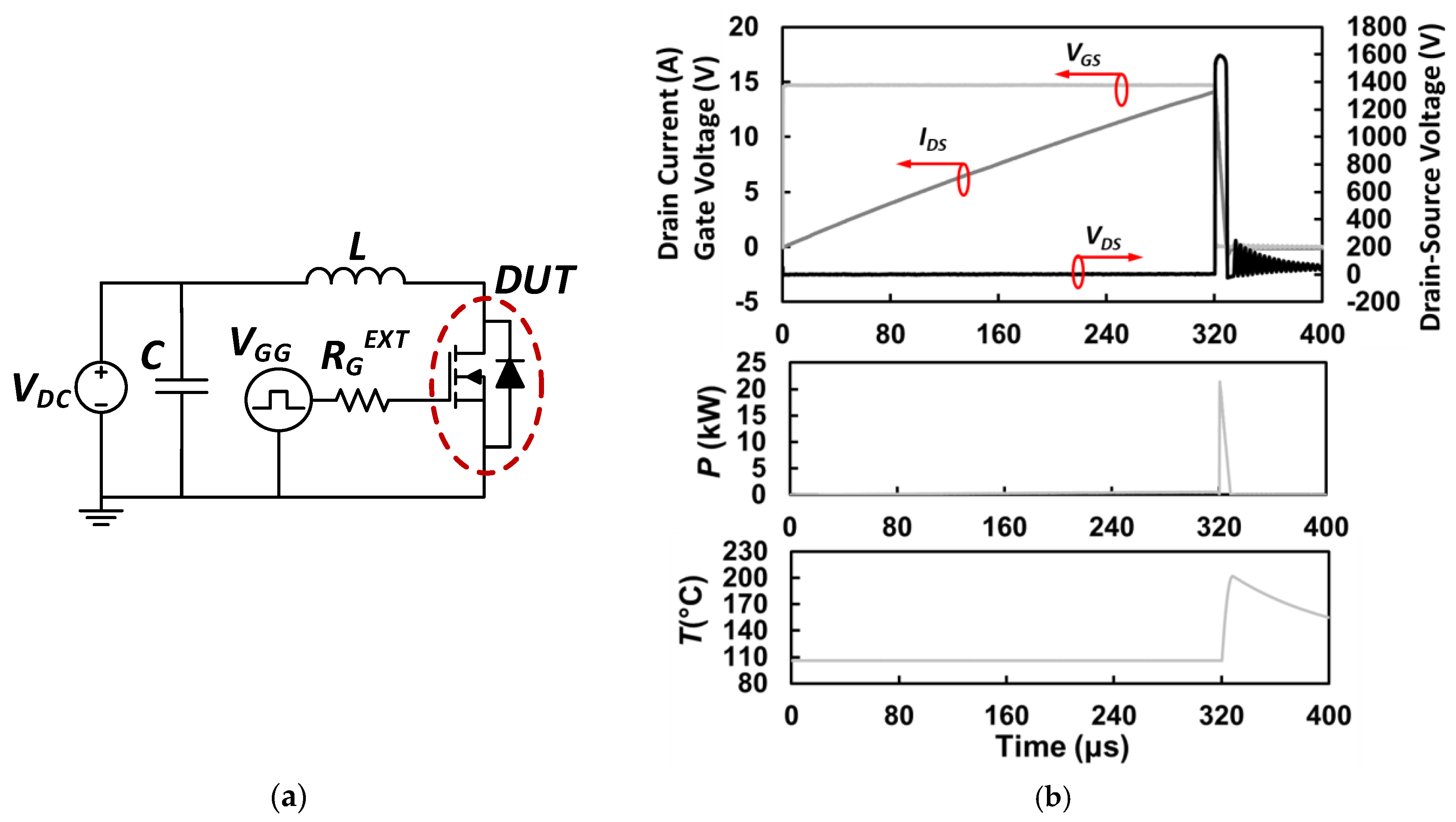
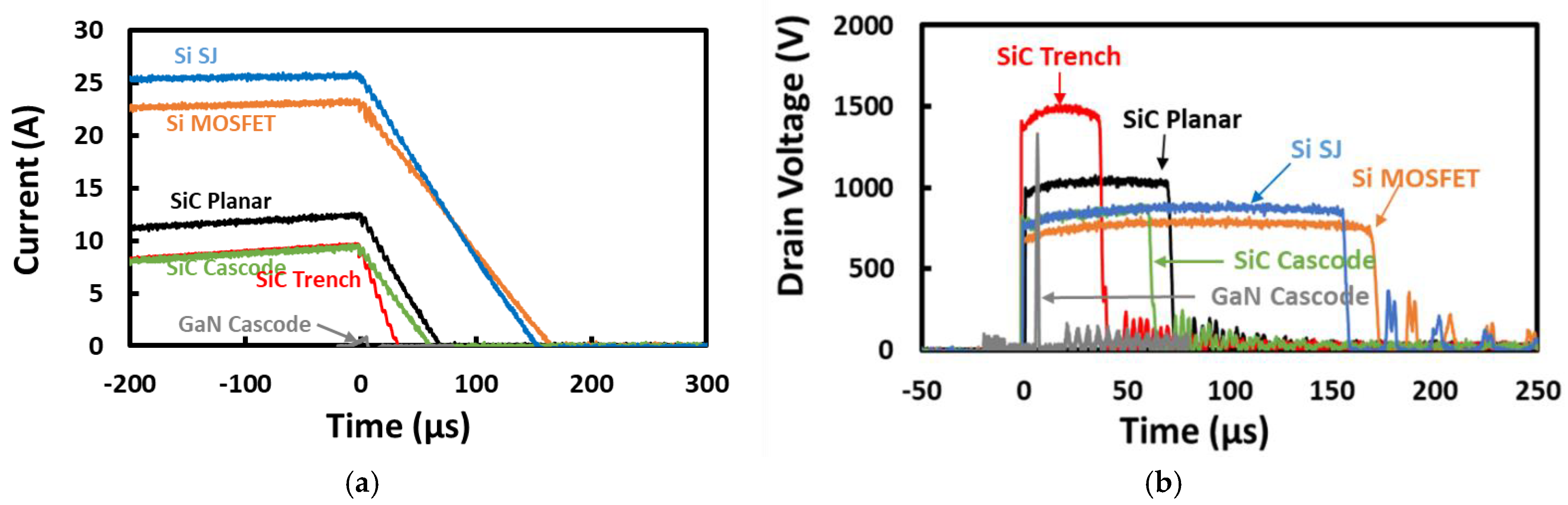
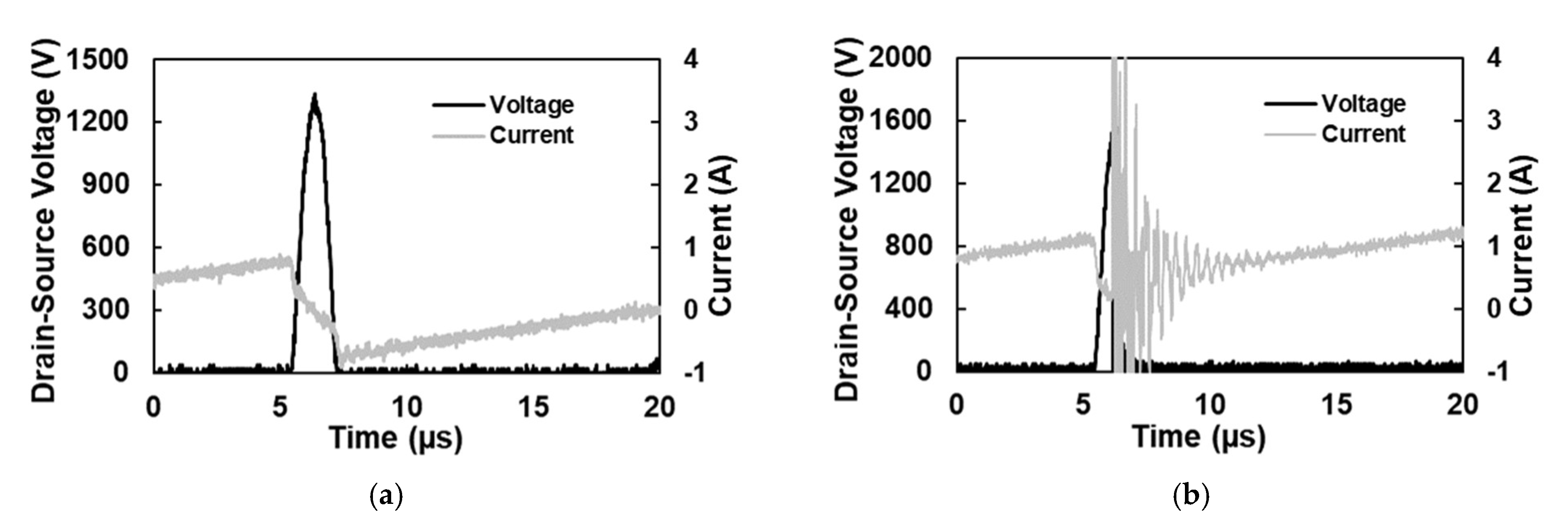
3.2. Short Circuit Robustness

The short circuit (SC) ruggedness of a power device is an important reliability metric, as it quantifies the capacity of the power device to withstand sudden energy surges resulting from anomalous operations leading to short circuits [53,54,55]. Devices operating under normal conditions will either block the voltage in the OFF state (with ideally zero current, but, in reality, there is a leakage current on the order of nanoamperes) or conduct current in the ON state (with ideally zero voltage drop, but, in reality, there is a voltage drop of a few volts). Under short circuit conditions, however, there is simultaneously high voltage across the device while it is conducting the full load current. This means that there is a very significant instantaneous power dissipation and high junction temperature. Short circuits can occur when two devices in the same phase leg are turned on (called a hard switching fault) or when there is a short circuit across the load (called Fault Under Load). The short circuit withstand time (SCWT) is the maximum time duration that a device can endure under short circuit conditions before electrothermal failure. The short circuit critical energy is the maximum short circuit energy the DUT can dissipate without failure.
Figure 10a shows a picture of the test rig for short circuit measurements, while Figure 10b shows the equivalent circuit of the test rig [56]. An example of the SC test characteristics is shown in Figure 10c. The circuit comprises of a DC power supply and DC link capacitor bank for emulating the HGV DC bus and a control IGBT module, which typically has a current rating several times (at least 10 times) larger than the current rating of the DUT transistor. The DC power supply charges up the DC link capacitor while the DUT and the control IGBT are off. The much larger output capacitance of the control IGBT means that the majority of the DC link voltage falls across the DUT as is the case in series-connected capacitors. The control IGBT turns on, and is followed by the DUT. The energy stored in the DC link capacitor bank is discharged through the control IGBT into the DUT. The control IGBT, which in this case is a 1.7 kV/1 kA silicon IGBT from Infineon with datasheet reference FF1000R17IE4, disconnects the DUT from the DC link if there is a short circuit failure. The on time of the DUT is increased by 500 nanosecond pulse steps until it fails. This has been conducted at three junction temperatures, namely 25 °C, 75 °C and 150 °C, using a Rogowski coil to measure the short-circuit current. The SC measurements are performed on three devices in each technology to ensure statistical integrity and that rogue devices do not disguise the analysis. The selected devices are 650 V rated and include a SJ MOSFET, Silicon IGBT, SiC Cascode JFET, SiC Trench MOSFET and SiC Planar MOSFET. The tests were performed at 400 V DC link voltage, and failure analysis details are provided in [57].
Figure 11a shows the last-pass (last SC measurement before failure) short circuit current transient for all device technologies at a case temperature of 25 °C, while Figure 11b shows similar measurements at 150 °C. As the short circuit current is drawn from a voltage source, it is limited by the temperature-dependent short circuit resistance of the DUT.
As can be observed from Figure 11, different device technologies have different peak currents due to differences in the short circuit resistance. The temperature coefficient of the short circuit resistance determines how steep the decline from the peak short current is with time. The silicon SJ MOFET and IGBT have the highest peak SC currents, with the SiC devices having smaller currents. This is due to the higher short circuit resistance of the SiC MOSFETs. Figure 12a,b shows the SCWT and Critical SC Energy for the different technologies at the different junction temperatures. The best performing devices in terms of SCWT are the Si SJ MOSFET and the SiC Trench MOSFET, followed by the Si IGBT, SiC Planar and SiC Cascode JFETs.
Several studies into the short circuit performance of SiC MOSFETs have demonstrated reduced SCWT compared to silicon MOSFETs due to increased thermal impedance (from smaller die sizes) and reduced oxide robustness (from the increased interface and fixed oxide charge) [58,59,60,61]. An important factor in determining the SCWT is the die area, since the peak junction temperature will reduce with an increasing die area. This is because thermal impedance is inversely proportional to die size; hence, a larger area device will more likely have a longer SCWT. Figure 13a shows the SCWT as a function of the die size for each of the device technologies. Except for the SiC Trench MOSFET, the SCWT is proportional to die size. The SiC Trench MOSFET appears to have very good short circuit ruggedness, given that it has a smaller chip area compared to the SJ MOSFET and Si IGBT. Figure 13b shows the SCWT as a function of the switching energy in each device technology where there is a trade-off between SCWT and switching energy.
The high performance of the Silicon SJ MOSFET is due to a large die size which comes with higher switching energy, since device capacitances increase with die size. The SiC Cascode JFET which has the best switching performance also has the lowest SCWT (hence, it is least short-circuit-rugged). The short circuit performance of 650 GaN HEMTs has been reported in the literature, with very short durations (less than 1 µs) for DC link voltages of 400 V [62,63,64]. Oscillations during the short circuit event in GaN Cascodes have been reported in [63,65].

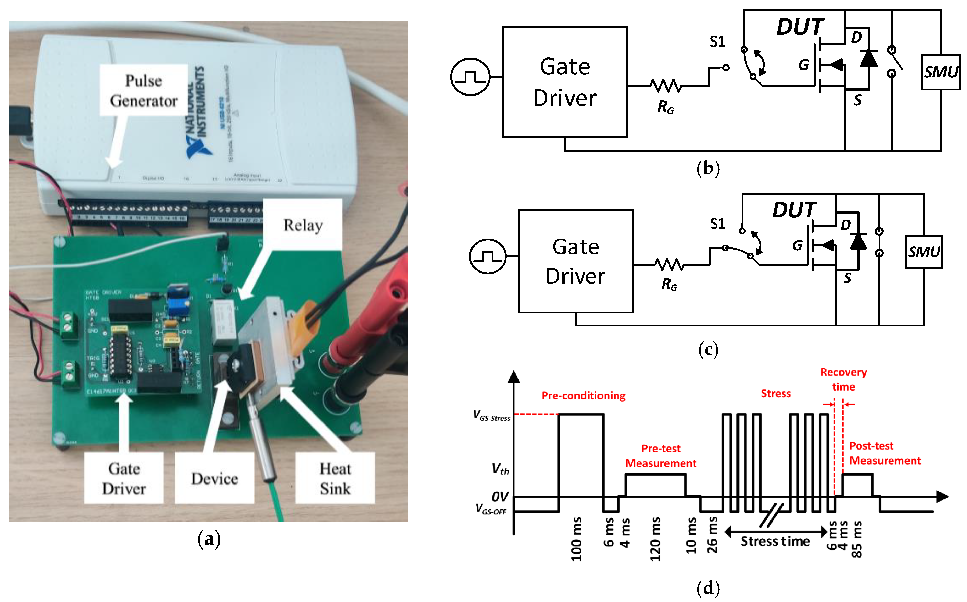
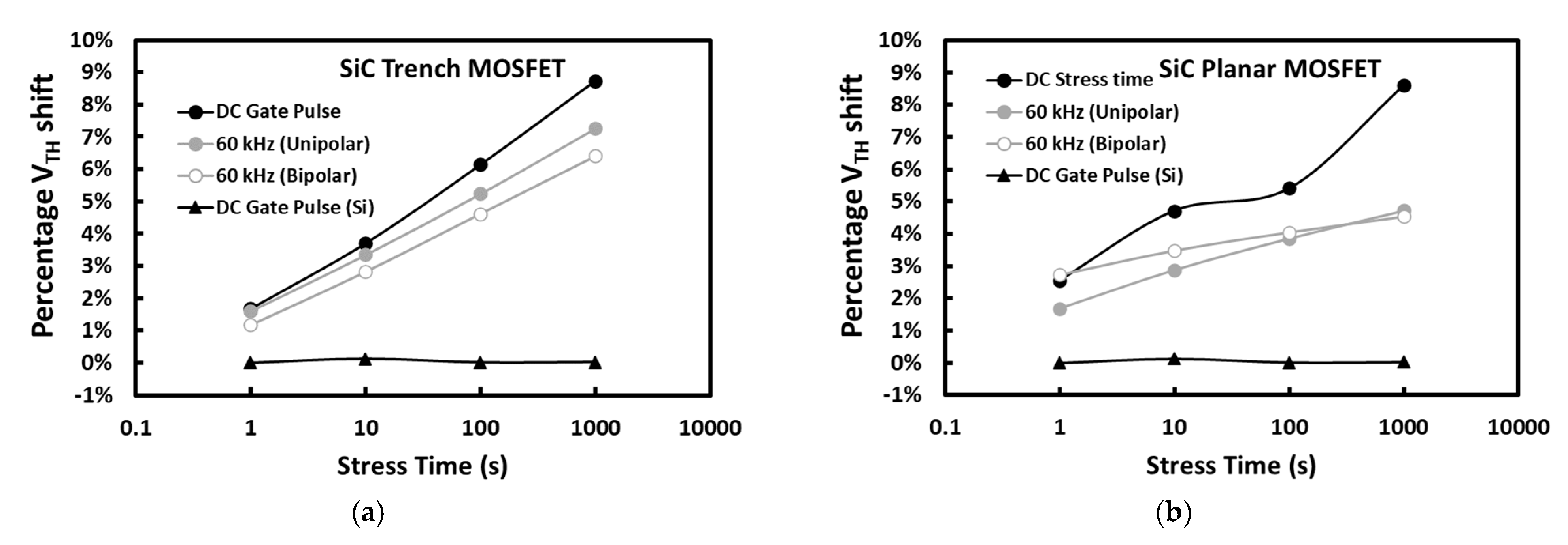
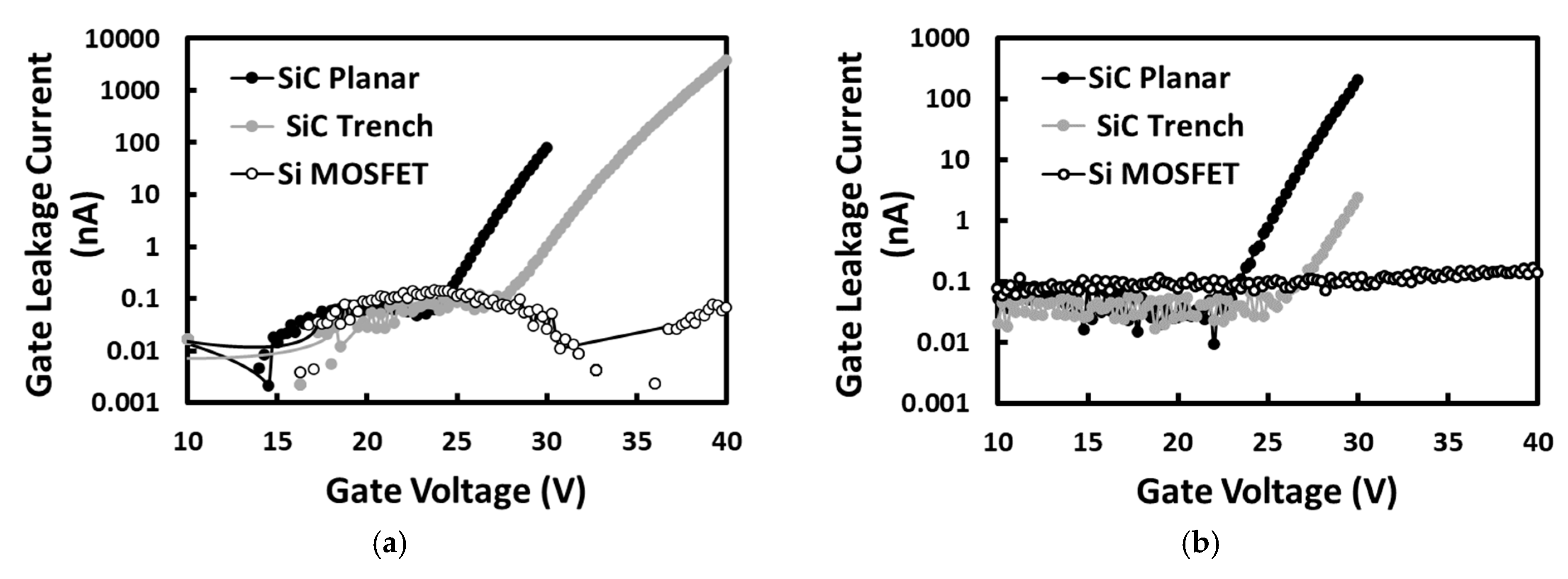
3.3. Gate Oxide Reliability Performance

Gate oxide reliability refers to the ability of the MOSFET/IGBT gate to retain its insulating properties required for controlling the device. In power electronics, particularly for automotive applications, there are strict reliability standards set out by industrial organisations such as the Joint Electron Device Engineering Council (JEDEC) [66] and the Automotive Electronics Council (AEC) [67]. These standards stipulate that power semiconductor devices must pass a series of tests, one of which includes high temperature gate bias (HTGB). HTGB involves biasing the gate of the power device with its rated drive voltage for 1000 h at a high temperature (175 °C). For the device to pass, none of its parameters (threshold voltage, gate leakage current, drain leakage current, on-state resistance, etc.) should deviate from the pre-test values by more than a predefined amount. These tests have been performed in silicon devices (MOSFETs and IGBTs) over several years; hence, most issues pertaining to the gate oxide reliability in silicon devices have been resolved. However, new devices such as SiC MOSFETs have faced some challenges, particularly regarding the issue of Bias Temperature Instability (BTI). BTI refers to a process where the threshold voltage of the device shifts (usually by millivolts) depending on the magnitude and polarity of a gate stress voltage. Several researchers have reported on BTI in SiC MOSFETs [68,69,70,71,72,73], demonstrating that VTH is less stable compared to silicon devices. When a positive VGS stress is applied to the MOSFET, VTH shifts upwards because of negative charge trapping; when a negative VGS stress is applied, VTH shifts downwards because of positive charge trapping. Unlike Si MOSFETs, the charge trapping and release time constants are much shorter; hence, the post-stress-measured VTH depends on the time between the stress removal and VTH measurement. This has resulted in new HTGB guidelines and test procedures and guidelines specific to wide bandgap devices [74,75].
Gate oxide reliability is even more important for HGV applications because paralleling several power devices requires good current sharing and electrothermal stability. Variations of VTH across parallel devices can cause reliability problems due to poor current sharing under extreme conditions, for example, in short circuits [76,77]. In the study performed in this review, BTI is assessed in the power devices by performing HTGB measurements using the classic measure–stress–measure sequence with bipolar preconditioning before each sequence; i.e., VTH is measured before VGS stress and after VGS stress at pred-defined intervals. Bipolar preconditioning simply means that a VGS pulse of both positive and negative polarity is applied to the device gate for a defined duration (usually 10 milliseconds). This is different from the VGS stress and is conducted to set an initial charge state in the gate oxide which is to act as a reference for subsequent measurements.
Figure 14a shows a picture of the test set-up including the gate driver, the DUT and other ancillary components for enabling the test, including a National Instruments DAQ Board to generate the control pulses and an adjustable gate driver for performing the gate stress. Figure 14b shows the equivalent circuit of the test set-up in Figure 14a under a VTH measurement mode. VTH is measured by connecting the gate and drain of the MOSFET while forcing a 1 mA drain-source current through the channel using a source measurement unit (SMU). In these measurements, the SMU is a model 2602 B from Keithley that is controlled using LabVIEW. Figure 14c shows the test set-up in the VGS stress mode where the drain and source are connected (to ensure VDS is zero), and the gate is connected to a gate driver which supplies the stress VGS voltage at a given magnitude and frequency. Figure 14d shows the stress–measure–stress gate pulse sequence, including the pre-conditioning, which is implemented to reset the charges on the MOSFET gate.
The BTI analysis presented here is conducted for a DC stress pulse (constant VGS stress), unipolar VGS stress pulses at 60 kHz (VGS is switched from 0 to a rated value) and the bipolar VGS stress pulses at 60 kHz (VGS is switched from −5 V to a rated value). The results are shown in Figure 15a for the SiC Trench MOSFET and Figure 15b for the SiC Planar MOSFET. Both devices are compared to measurements obtained from a silicon MOSFET. It should be noted here that a SiC Cascode JFET comprises a low voltage silicon MOSFET as the input; hence, BTI tests performed on a SiC Cascode JFET investigate the gate characteristics of the low voltage silicon MOSFET. It is clear from Figure 15a,b that the VTH shifts in Silicon MOSFETs are negligible compared to that in both SiC MOSFETs, which can increase by up to 9% after 1000 s of DC and pulsed stresses. The shift in the VTH of the SiC MOSFETs is due to negative charge trapping, which increases with time. As the shift is evident after post-test bipolar preconditioning, it can be considered to be a permanent shift in VTH.
Figure 16 shows the results of the oxide breakdown voltage tests. This is conducted by simply increasing the gate voltage on the gate oxide until it breaks down and becomes unable to support the voltage without a rapid increase in the gate leakage current. Figure 16a shows the test results for a SiC Planar and a Trench MOSFET compared with a silicon SJ MOSFET at 25 °C, while Figure 16b shows similar test results at 150 °C. Figure 16 shows that the silicon MOSFET gate oxide is more robust at higher voltages compared to the selected SiC MOSFETs, which break down at 23 V for the selected Planar MOSFET and 27 V for the selected Trench MOSFET. The silicon MOSFET oxide retains its insulating properties beyond 40 V. These measurements demonstrate that the fixed oxide and interface trapped charge in SiC MOSFETs means that the gate oxide is not as robust against high voltages, as is the case in silicon MOSFETs. VTH is also more stable in silicon MOSFETs compared to SiC MOSFETs.

3.4. Avalanche Ruggedness Performance

Some applications require devices to operate repetitively under unclamped inductive switching (UIS) conditions, for example, in automotive fuel injection systems. Although devices in EV chargers and traction inverters do not require the repetitive operation of devices under UIS, it is nevertheless necessary to evaluate the avalanche ruggedness of power devices under UIS because some failure modes result in the latching of the MOSFET parasitic BJT. Examples include cosmic ray-induced failures, anti-parallel diode failure or hard commutation of the body diode with high dV/dt and dI/dt. There have been several studies into the avalanche ruggedness of SiC MOSFETs, all of which allude to the wide bandgap properties as being advantageous for improved performance [78,79,80,81,82]. The avalanche ruggedness of power MOSFETs is tested by subjecting the devices to unclamped inductive switching. The failure mode is either (i) the latching of the parasitic BJT in the MOSFET causing thermal runaway through current hot-spots or (ii) thermal limit breaching of the average device junction temperature. The first failure mode results from the large avalanche power dissipated in the device over a short duration, while the second failure mode results from the smaller avalanche power dissipated in the device over a longer duration. All the 650 V devices in this study have been tested under UIS using the circuit shown in Figure 17a [52]. The DC supply voltage VDC was 50 V, and the inductor L was 6 mH, except for the GaN cascode HEMT, which was tested using a 1 mH inductor. Figure 17b shows the typical avalanche characteristics observable in a UIS measurement. The gate voltage (VGS) of the DUT is turned on, thereby causing the current to rise at a rate given by VDC/L. After a pre-defined time interval, the DUT is turned off, causing the energy stored in the magnetic field of the inductor to discharge into DUT while it is off. As the DUT is off and there is no channel for the current to flow through, the DUT goes into an avalanche as the current flows through the impact ionisation. During this period, the drain-source voltage of the DUT is at its breakdown value, which is usually higher than the datasheet rating of the device, depending on how much the manufacturers have de-rated. This causes a junction temperature surge such as the one observed in a short circuit. To measure the avalanche ruggedness of the DUT, the VGS pulse duration is increased, therefore increasing the avalanche current and power, until the DUT fails. This is conducted at different initial junction temperatures to gauge the thermal activation of the parasitic BJT for each device technology. The maximum energy the DUT can dissipate under the avalanche quantifies the avalanche ruggedness of the MOSFET technology.
For studying the UIS performance, the following 650 V rated devices were selected: two Si super-junction MOSFETs with datasheet references IPW65R080CFDA and SIHG33N60EF, a SiC planar MOSFET with reference C3M006065D, a SiC Cascode JFET with datasheet reference UJ3C065080K3S, a SiC trench MOSFET with reference SCT3080AL and a GaN Cascode HEMT with datasheet reference TP65H050WS.
Figure 18a shows the last pass avalanche current transients of all of the DUTs (except the Si SJ MOSFET), while Figure 18b shows the corresponding avalanche voltage transients of the DUTs. It should be noted that the maximum avalanche energy of the Si SJ MOSFET could not be reached (the limits of the test set-up were exceeded); hence, the measurements are not indicative of its avalanche ruggedness, which is the highest for all of the technologies. It is interesting to note that the different MOSFET technologies, although all rated at 650 V according to their respective datasheets, have different actual breakdown voltages. The SiC Trench MOSFET has the highest breakdown voltage at approximately 1500 V, followed by the SiC Planar MOSFET at 1000 V, the Si SJ MOSFET at 915 V, the Cascode JFET at 900 V and the silicon MOSFET at 830 V.
The GaN cascode does not have UIS capability and fails at very low avalanche currents (even for 1 mH inductor at ambient temperature). The current and voltage transients of the last pass and failure (at a current of 1 A) are shown in Figure 19, whereas the failure mechanism is discussed in [83].
Figure 20a shows the peak avalanche current normalised by the 25 °C current rating of the device while Figure 20b shows the measured critical avalanche energy at 25 °C, 75 °C and 150 °C. The results for the Si SJ MOSFET are not presented because the critical avalanche energy of the device exceeded the capacity of the test circuit. Hence, the Si SJ MOSFET demonstrated their best avalanche ruggedness performance. The results demonstrate that the silicon devices (MOSFET and silicon SJ) are more avalanche rugged than the SiC MOSFETs as their maximum avalanche currents and energies are larger than the SiC MOSFETs. This is due to lower thermal impedance resulting from larger die size, hence, lower instantaneous junction temperatures. As the chip sizes of SiC devices are 5 to 10 times smaller than Si devices [56,84,85], from a material evaluation point of view, some studies [56,85] consider the avalanche energy density. However, from the application point of view, the avalanche energy is a more relevant metric.

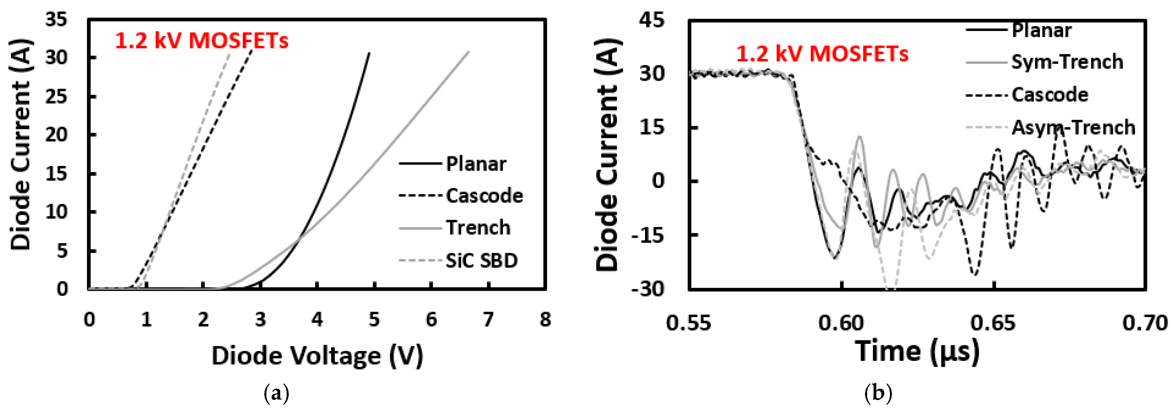
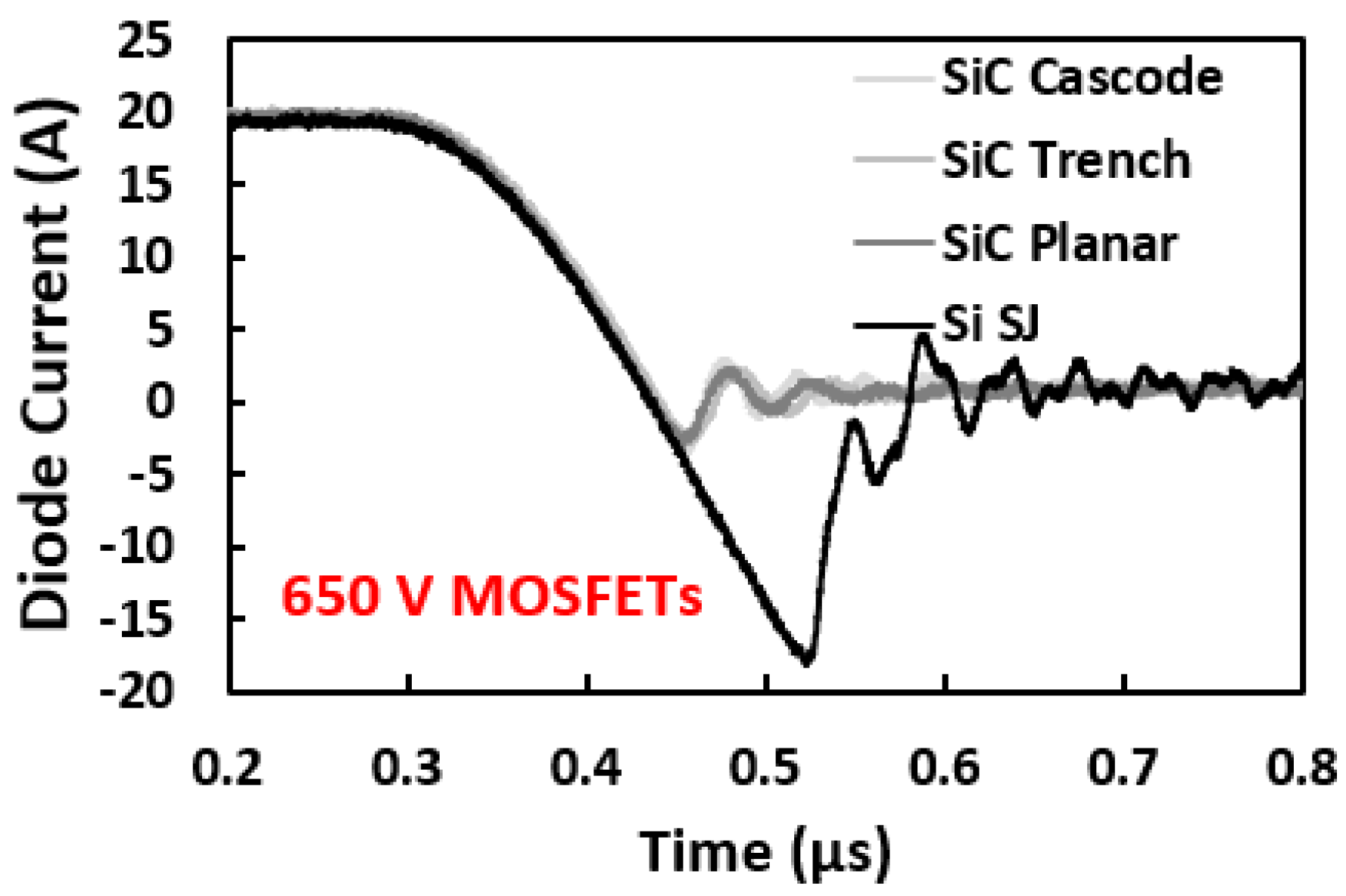
3.5. Body Diode Performance

Body diodes are important for dead-time operation and regenerative breaking when the traction converter operates as a rectifier, converting the AC power generated by the electrical machine into DC power to recharge the battery. Body diode characteristics also contribute to the switching performance of power devices, since the stored charge will contribute to switching losses [86,87]. Between 650 V and 1.2 kV, it is customary to use SiC Schottky Barrier Diodes (SBDs) because of the excellent switching performance. SiC SBDs have very little stored charge since they are a majority carrier unipolar device, unlike PiN diodes that are minority carrier bipolar devices. Another advantage of SiC SBDs is that the switching losses are temperature invariants, unlike Silicon PiN diodes that have switching losses that increase with temperature due to the positive temperature coefficient of the minority carrier lifetime [88]. However, MOSFET body diodes can also be used instead of SiC SBDs, with the advantage of a reduced component account and improved power module compactness. However, body diodes are PiN diodes since the voltage blocking drift region is between the p-body anode and the heavily doped N+ cathode. This means that there is some stored charge, although not as much as silicon PiN diodes because of the reduced minority carrier lifetime in SiC compared to silicon [86]. Figure 21a shows the measured forward voltage characteristics for 1.2 kV SiC Planar MOSFET, SiC Trench MOSFETs, SiC Cascode JFETs and a reference SiC SBD. The results in Figure 21a demonstrate the third quadrant forward characteristics of the SiC SBD, and the SiC Cascode JFET demonstrate a better conduction performance compared to the Planar and Trench SiC MOSFETs. The absence of the PN junction in the SiC SBD means that by tuning the Schottky metal work function, low forward voltages can be achieved compared with MOSFET body diodes. The good performance of the third quadrant characteristics of the SiC Cascode JFET is because the diode characteristics are that of the low voltage Silicon MOSFET and not a SiC MOSFET (hence the narrower bandgap of silicon compared to SiC ensures a lower junction voltage). The smaller bandgap of silicon compared to SiC means that the junction voltage is lower because of the higher intrinsic carrier concentration. Low junction voltage is good for conduction loss. However, when it comes to switching loss, the reverse recovery characteristics of the body diode are important. Figure 21b shows the reverse recovery characteristics of the body diodes extracted from switching measurements. The peak negative current at turn-off is a combination of some stored charge and PN junction capacitance. The ringing in the measurements is due to electromagnetic resonance between the device junction capacitance and parasitic inductance in the current flow path. A peak negative current of 15 A is measured for a forward current of 30 A. This will contribute to the turn-on switching losses of the transistor into which the diode is commutating the current.
Figure 22 shows the reverse recovery characteristics of 650 V SiC Planar, Trench, Cascode devices in comparison with a silicon super-junction MOSFET [52]. The performance of the body diodes of the SiC MOSFETs at 650 V is improved with a reduced peak negative current. It can be observed from Figure 22 that the body diode performance of the SiC devices is considerably better, with a significantly smaller peak negative current compared to the silicon SJ MOSFET. The switching frequency of the application will ultimately determine which technology yields a better body diode performance. At low switching frequencies where body diode conduction losses dominate, it would be advisable to use a technology with a low forward voltage (SiC SBD or silicon MOSFET body diode). At high switching frequencies where switching losses dominate, it would be advisable to use a technology with a low stored charge and reverse currents (SiC SBD, SiC MOSFET body diode at 650 V and SiC SBD at 1.2 kV).

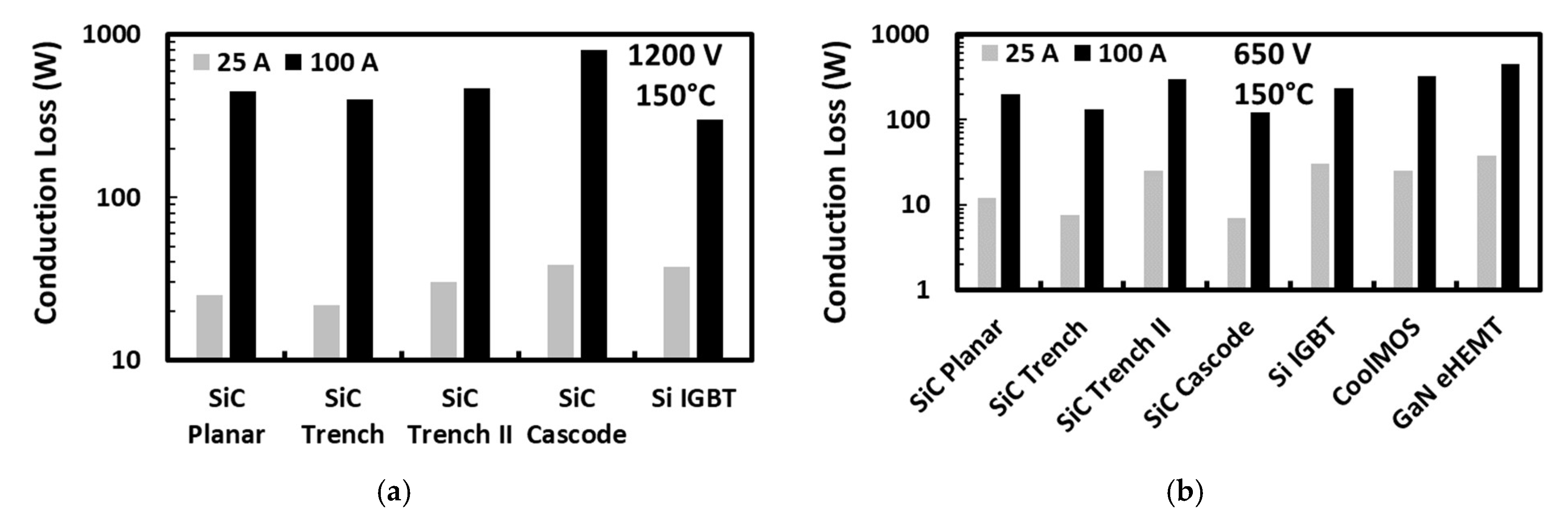
3.6. Conduction Performance

Conduction losses are very important, as they are the dominant losses in power electronic converters operated with low to intermediate switching frequencies. In EV powertrains, the fundamental frequency of the converter will determine the rotational speed of the motor, which in turn depends on the demanded power and the number of motor poles. Typical motor speeds can range from 8000 to 20,000 rpm and fundamental frequencies between 500 Hz and 1 kHz [89]. Assuming a minimum switching frequency that is 10 times the fundamental frequency, this means a device switching frequency of approximately 10 kHz at top speed. While SiC MOSFETs will yield better switching losses than Si IGBTs, the comparison of the conduction losses between the two technologies is less straight forward, especially at 1.2 kV. Under low speed and high torque conditions, for example during starting or a motor stall, the power devices will operate with low fundamental frequencies and close to a full load (high current). Under these conditions, conduction losses are dominant. In high-speed low torque conditions, conduction losses are less dominant. In this paper, using power device datasheets, the conduction losses have been calculated for the different power device technologies at 650 V and 1.2 kV ratings. The devices under comparison all have similar current ratings. The conduction losses are calculated using the device forward characteristics (or on-resistance vs. current characteristics) at 150 °C to 175 °C for a 100 A and 25 A load current. The high junction temperature is used to account for worst case conditions. Figure 23a shows the results of these calculations for 1.2 kV rated devices, while Figure 23b shows the results for 650 V rated devices. The results for 1.2 kV devices demonstrate that the silicon IGBT has the best projected performance (lowest conduction loss) at 100 A, while the SiC MOSFETs perform marginally better at 25 A. SiC MOSFETs usually have lower conduction losses compared to similarly rated silicon IGBTs at low currents, while the IGBTs have lower conduction losses at high currents. This is because the IGBTs have a knee-voltage Vknee due to the PN junction at the collector, while MOSFETs do not have this knee voltage. The equations for the conduction losses for MOSFETs and IGBTs are shown below, where RCE is the slope ΔVCE/ΔICE.
P C O N _ M O S F E T = i D S 2 R D S
P C O N _ I G B T = i C E V C E o n = i C E V k n e e + i C E R C E
Figure 23b shows that for 650 V devices at 150 to 175 °C junction temperatures, silicon IGBTs have comparable losses with the SiC MOSFETs at 100 A and 25 A load currents. Figure 23b includes GaN e-HEMTs (with datasheet reference GS66516T) as well as a silicon superjunction MOSFET(CoolMOSTM). The results in Figure 23 demonstrate that silicon IGBTs are comparable to advanced WBG devices in terms of conduction losses and even outperform them at high load currents at a 1.2 kV level. It has been proposed by some researchers to combine SiC MOSFETs and IGBTs in hybrid switches to exploit the advantages of both technologies [90,91,92]. In these hybrid switches, the SiC MOSFETs will perform the switching and low current conduction operation, while the silicon IGBTs will perform the full load current operation. This solution also has cost benefits, given that silicon IGBTs are considerably cheaper than SiC MOSFETs.

4. Conclusions

Power electronic devices are critical for HGV electrification. HGV chargers and traction inverters require highly reliable and energy efficient power devices for energy conversion. The voltage classes of the devices used are between 650 V and 1200 V. The devices include SiC Trench MOSFETs, SiC Planar MOSFETs, SiC Cascode JFETs, silicon SJ MOSFETs, silicon IGBTs, GaN e-HEMTs and GaN Cascode HEMTs. There are many metrics involved in power device selection, including efficiency, reliability and cost. In this review, the latest generation devices from leading manufacturers have been assessed in terms of efficiency and their reliability. The switching energies of 650 V and 1200 V rated devices were measured along with their short circuit ruggedness, gate oxide robustness, third quadrant performance and avalanche ruggedness under UIS. Table 1 summarises the findings.
For EV charger applications where high switching frequencies are used in Vienna rectifiers and soft-switched DC/DC converters, the high switching losses and longer gate delays in IGBTs make them not optimal for this application. GaN Cascode HEMTs and e-HEMTs would be good candidates given their excellent switching characteristics; however, the poor performance in short circuit conditions and lack of avalanche ruggedness makes them electrothermally fragile. Silicon SJ MOSFETs have higher switching losses than SiC MOSFETs and Cascode JFETs given the higher capacitances due to larger die sizes. SiC Cascode JFETs have excellent switching performance; however, they are limited in short circuit ruggedness compared to SiC Trench MOSFETs. It should be noted that SiC Cascode JFETs completely avoid oxide robustness and threshold voltage shifting problems in SiC MOSFETs. In this application, the SiC Planar, Trench MOSFETs and Cascode JFETs best meet the requirements of reliability and efficiency. At the 650 V level (for Vienna rectifiers and traction inverters at 400 V DC bus), the body diode of the SiC MOSFET can be used; however, at the 1.2 kV level (for DC/DC converters and a traction inverter for 800 V DC bus), it is advisable to use SiC SBDs.
For the HGV traction inverter, although Silicon MOSFETs and IGBTs provide the best performance in terms of the gate oxide robustness and avalanche ruggedness, they have higher switching losses compared to SiC MOSFETs and GaN devices. However, if switching frequencies are low enough for conduction losses to dominate, then the switching loss is inconsequential. Silicon IGBTs have a better conduction loss performance at the full load current, while SiC MOSFETs and GaN devices have a marginally better conduction loss performance at low load currents. An optimal solution could be a hybrid switch that contains Si IGBTs in parallel with SiC MOSFETs. GaN e-HEMTs and GaN Cascodes have a limited commercial availability at the 1200 V rating; hence, they are not widely considered for 800 V traction inverter applications. The conduction loss performance of GaN is not better than IGBTs or SiC MOSFETs. Furthermore, the limited short circuit robustness, avalanche ruggedness and electrothermal performance in current GaN technologies means they are not reliable enough to implement high power traction inverters, especially given the heat management requirements. SiC Cascode JFETs have excellent switching performances but a marginally reduced short circuit and avalanche performance compared to SiC Planar and Trench MOSFETs. The best solution for the traction inverter in terms of losses and reliability remains the silicon IGBT with an anti-parallel SiC SBD for reverse conduction.
Upcoming challenges: This review has characterised the main power device technologies suitable for HGV applications. Nevertheless, considering the converter implementation, other challenges include EMI/EMC [93,94,95], investigating the impact of high voltage commutation rates on motor insulation reliability [96,97,98], power module/converter designs involving multiple chips in parallel and optimised busbars [99,100,101], thermal management and increased power densities [102,103], short circuit detection [104,105] and application-specific qualification methodologies/guidelines, as suggested by the JEDEC JC-70 guidelines and the ECPE guidelines for the qualification of power modules used in motor vehicles (AQG 324) [106]. The increased commercial availability of higher voltage devices (1.7 kV to 3.3 kV rated) may open new avenues for higher voltage charger designs and even higher inverter bus voltages. The investigations summarised in this review are also applicable to electric and hybrid ships, as well as agricultural machinery.

Funding

This research received no external funding.

Data Availability Statement

Not applicable.

Conflicts of Interest

The authors declare no conflict of interest.

References

  1. Grid, N. Government Plans, Commitments and Targets. Available online: https://www.nationalgrid.com/responsibility/environment/decarbonising-transport/heavy-goods-vehicles (accessed on 22 May 2023).
  2. Manthiram, A. An Outlook on Lithium Ion Battery Technology. ACS Cent. Sci. 2017, 3, 1063–1069. [Google Scholar] [CrossRef] [PubMed]
  3. Impact of Transport on Energy Consumption and the Environment, Including Electric Vehicle Charging, Greenhouse Gas Emissions and Air Pollution. Available online: https://www.gov.uk/government/collections/energy-and-environment-statistics (accessed on 22 May 2023).
  4. Perumal, S.S.; Lusby, R.M.; Larsen, J. Electric bus planning & scheduling: A review of related problems and methodologies. Eur. J. Oper. Res. 2022, 301, 395–413. [Google Scholar] [CrossRef]
  5. Aldenius, M.; Mullen, C.; Pettersson-Löfstedt, F. Electric buses in England and Sweden—Overcoming barriers to introduction. Transp. Res. Part D Transp. Environ. 2022, 104, 103204. [Google Scholar] [CrossRef]
  6. Mahmoud, M.; Garnett, R.; Ferguson, M.; Kanaroglou, P. Electric buses: A review of alternative powertrains. Renew. Sustain. Energy Rev. 2016, 62, 673–684. [Google Scholar] [CrossRef]
  7. Liimatainen, H.; van Vliet, O.; Aplyn, D. The potential of electric trucks—An international commodity-level analysis. Appl. Energy 2019, 236, 804–814. [Google Scholar] [CrossRef]
  8. Smallbone, A.; Jia, B.; Atkins, P.; Roskilly, A.P. The impact of disruptive powertrain technologies on energy consumption and carbon dioxide emissions from heavy-duty vehicles. Energy Convers. Manag. X 2020, 6, 100030. [Google Scholar] [CrossRef]
  9. Haugen, M.J.; Flynn, D.; Greening, P.; Tichler, J.; Blythe, P.; Boies, A.M. Electrification versus hydrogen for UK road freight: Conclusions from a systems analysis of transport energy transitions. Energy Sustain. Dev. 2022, 68, 203–210. [Google Scholar] [CrossRef]
  10. Li, K.; Acha, S.; Sunny, N.; Shah, N. Strategic transport fleet analysis of heavy goods vehicle technology for net-zero targets. Energy Policy 2022, 168, 112988. [Google Scholar] [CrossRef]
  11. Börjesson, M.; Johansson, M.; Kågeson, P. The economics of electric roads. Transp. Res. Part C Emerg. Technol. 2021, 125, 102990. [Google Scholar] [CrossRef]
  12. Samet, M.J.; Liimatainen, H.; van Vliet, O.P.; Pöllänen, M. Road Freight Transport Electrification Potential by Using Battery Electric Trucks in Finland and Switzerland. Energies 2021, 14, 823. [Google Scholar] [CrossRef]
  13. Williamson, S.S.; Rathore, A.K.; Musavi, F. Industrial Electronics for Electric Transportation: Current State-of-the-Art and Future Challenges. IEEE Trans. Ind. Electron. 2015, 62, 3021–3032. [Google Scholar] [CrossRef]
  14. Khaligh, A.; D’Antonio, M. Global Trends in High-Power On-Board Chargers for Electric Vehicles. IEEE Trans. Veh. Technol. 2019, 68, 3306–3324. [Google Scholar] [CrossRef]
  15. Tu, H.; Feng, H.; Srdic, S.; Lukic, S. Extreme Fast Charging of Electric Vehicles: A Technology Overview. IEEE Trans. Transp. Electrif. 2019, 5, 861–878. [Google Scholar] [CrossRef]
  16. Papamanolis, P.; Krismer, F.; Kolar, J.W. 22 kW EV Battery Charger Allowing Full Power Delivery in 3-Phase as well as l-Phase Operation. In Proceedings of the 2019 10th International Conference on Power Electronics and ECCE Asia (ICPE 2019—ECCE Asia), Busan, Korea, 27–30 May 2019; pp. 1–8. [Google Scholar]
  17. Anderson, J.A.; Haider, M.; Bortis, D.; Kolar, J.W.; Kasper, M.; DeBoy, G. New Synergetic Control of a 20kW Isolated VIENNA Rectifier Front-End EV Battery Charger. In Proceedings of the 2019 20th Workshop on Control and Modeling for Power Electronics (COMPEL), Toronto, ON, Canada, 17–20 June 2019; pp. 1–8. [Google Scholar]
  18. Aretxabaleta, I.; Alegría, I.M.D.; Andreu, J.; Kortabarria, I.; Robles, E. High-Voltage Stations for Electric Vehicle Fast-Charging: Trends, Standards, Charging Modes and Comparison of Unity Power-Factor Rectifiers. IEEE Access 2021, 9, 102177–102194. [Google Scholar] [CrossRef]
  19. Soeiro, T.; Friedli, T.; Kolar, J.W. Three-phase high power factor mains interface concepts for Electric Vehicle battery charging systems. In Proceedings of the 2012 Twenty-Seventh Annual IEEE Applied Power Electronics Conference and Exposition (APEC), Orlando, FL, USA, 5–9 February 2012; pp. 2603–2610. [Google Scholar]
  20. Abbasi, M.; Lam, J. An Interleaved Bridgeless AC/DC Stacked SiC Switches Based LLC Converter with Semi-Active Rectifiers for EV High Voltage Battery Systems. In Proceedings of the 2021 IEEE Energy Conversion Congress and Exposition (ECCE), Vancouver, BC, Canada, 10–14 October 2021; pp. 1853–1859. [Google Scholar]
  21. Yan, Y.; Bai, H.; Yang, C.; Wang, W. Securing Full-load-range Zero Voltage Switching for A Dual Active Bridge Based Electric Vehicle Charger. In Proceedings of the in 2020 IEEE Applied Power Electronics Conference and Exposition (APEC), New Orleans, LA, USA, 15–19 March 2020; pp. 2067–2072. [Google Scholar]
  22. Gill, L.; Ikari, T.; Kai, T.; Li, B.; Ngo, K.; Dong, D. Medium Voltage Dual Active Bridge Using 3.3 kV SiC MOSFETs for EV Charging Application. In Proceedings of the 2019 IEEE Energy Conversion Congress and Exposition (ECCE), Baltimore, MD, USA, 29 September–3 October 2019; pp. 1237–1244. [Google Scholar]
  23. Jiang, C.; Lei, B.; Teng, H.; Bai, H.K. The power-loss analysis and efficiency maximization of a silicon-carbide MOSFET based three-phase 10kW bi-directional EV charger using variable-DC-bus control. In Proceedings of the 2016 IEEE Energy Conversion Congress and Exposition (ECCE). IEEE J. Emerg. Sel. Top. Power Electron. 2016, 4, 880–892. [Google Scholar]
  24. Steinke, J.K.; Maibach, P.; Ortiz, G.; Canales, F.; Steimer, P. MVDC Applications and Technology. In Proceedings of the PCIM Europe 2019; International Exhibition and Conference for Power Electronics, Intelligent Motion, Renewable Energy and Energy Management, Nuremberg, Germany, 7–9 May 2019; pp. 1–8. [Google Scholar]
  25. Han, C.; Song, S.; Kim, J.; Jang, G. Enhancing Line Capacity Utilization in Power Transmission System Using Active MVDC Link. Energies 2019, 12, 1589. [Google Scholar] [CrossRef]
  26. Mura, F.; Doncker, R.W.D. Design aspects of a medium-voltage direct current (MVDC) grid for a university campus. In Proceedings of the 8th International Conference on Power Electronics—ECCE Asia, Jeju, Korea, 30 May–3 June 2011; pp. 2359–2366. [Google Scholar]
  27. Bathurst, G.; Hwang, G.; Tejwani, L. MVDC—The New Technology for Distribution Networks. In Proceedings of the 11th IET International Conference on AC and DC Power Transmission, Birmingham, UK, 10–12 February 2015. [Google Scholar]
  28. Sparacino, A.R.; Grainger, B.M.; Kerestes, R.J.; Reed, G.F. Design and simulation of a DC electric vehicle charging station connected to a MVDC infrastructure. In Proceedings of the 2012 IEEE Energy Conversion Congress and Exposition (ECCE), Raleigh, NC, USA, 15–20 September 2012; pp. 1168–1175. [Google Scholar] [CrossRef]
  29. Verma, A.; Mayank, K.; Meikap, S.; Kumar, C. Modelling and Control of Modular Multilevel Converter and Dual Active Bridge Based Fast Electric Vehicle Charger. In Proceedings of the 2022 4th International Conference on Energy, Power and Environment (ICEPE), Shillong, India, 29 April–1 May 2022; pp. 1–6. [Google Scholar] [CrossRef]
  30. Su, Y.-C.; Li, H.-M.; Chen, P.-L.; Cheng, P.-T. Integration of PV Panels and EV Chargers on the Modular Multilevel Converter Based SST. IEEE Trans. Ind. Appl. 2022, 58, 6428–6437. [Google Scholar] [CrossRef]
  31. Pouresmaeil, K.; Duarte, J.; Wijnands, K.; Roes, M.; Baars, N. Single-Phase Bidirectional ZVZCS AC-DC Converter for MVConnected Ultra-fast Chargers. In Proceedings of the PCIM Europe 2022; International Exhibition and Conference for Power Electronics, Intelligent Motion, Renewable Energy and Energy Management, Nuremberg, Germany, 10–12 May 2022; pp. 1–7. [Google Scholar]
  32. Issa, W.; Gonzalez, J.O.; Alatise, O. Design of a Gate-Driving Cell for Enabling Extended SiC MOSFET Voltage Blocking. Energies 2022, 15, 7768. [Google Scholar] [CrossRef]
  33. Sakaguchi, T.; Aketa, M.; Nakamura, T.; Nakanishi, M.; Rahimo, M. Characterization of 3.3 kV and 6.5 kV SiC MOSFETs. In Proceedings of the PCIM Europe 2017; International Exhibition and Conference for Power Electronics, Intelligent Motion, Renewable Energy and Energy Management, Nuremberg, Germany, 16–18 May 2017; pp. 1–5. [Google Scholar]
  34. Aghabali, I.; Bauman, J.; Emadi, A. Analysis of Auxiliary Power Unit and Charging for an 800V Electric Vehicle. In Proceedings of the in 2019 IEEE Transportation Electrification Conference and Expo (ITEC), Detroit, MI, USA, 19–21 June 2019; pp. 1–6. [Google Scholar]
  35. Jung, C. Power Up with 800-V Systems: The benefits of upgrading voltage power for battery-electric passenger vehicles. IEEE Electrif. Mag. 2017, 5, 53–58. [Google Scholar] [CrossRef]
  36. Aghabali, I.; Bauman, J.; Kollmeyer, P.J.; Wang, Y.; Bilgin, B.; Emadi, A. 800-V Electric Vehicle Powertrains: Review and Analysis of Benefits, Challenges, and Future Trends. IEEE Trans. Transp. Electrif. 2021, 7, 927–948. [Google Scholar] [CrossRef]
  37. Su, M.; Chen, C.; Sharma, S.; Kikuchi, J. Performance and cost considerations for SiC-based HEV traction inverter systems. In Proceedings of the 2015 IEEE 3rd Workshop on Wide Bandgap Power Devices and Applications (WiPDA), Blacksburg, VA, USA, 2–4 November 2015; pp. 347–350. [Google Scholar]
  38. Chou, W.; Kempitiya, A.; Vodyakho, O. Reduction of Power Losses of SiC MOSFET Based Power Modules in Automotive Traction Inverter Applications. In Proceedings of the in 2018 IEEE Transportation Electrification Conference and Expo (ITEC), Long Beach, CA, USA, 13–15 June 2018; pp. 1035–1038. [Google Scholar] [CrossRef]
  39. Hamada, K.; Nagao, M.; Ajioka, M.; Kawai, F. SiC—Emerging Power Device Technology for Next-Generation Electrically Powered Environmentally Friendly Vehicles. IEEE Trans. Electron Devices 2015, 62, 278–285. [Google Scholar] [CrossRef]
  40. Acquaviva, A.; Thiringer, T. Energy efficiency of a SiC MOSFET propulsion inverter accounting for the MOSFET’s reverse conduction and the blanking time. In Proceedings of the 2017 19th European Conference on Power Electronics and Applications (EPE’17 ECCE Europe). Warsaw, Poland, 11–14 September 2017; pp. P.1–P.9. [Google Scholar]
  41. Taha, W.; Nahid-Mobarakeh, B.; Bauman, J. Efficiency Evaluation of 2L and 3L SiC-Based Traction Inverters for 400 V and 800 V Electric Vehicle Powertrains. In Proceedings of the 2021 IEEE Transportation Electrification Conference & Expo (ITEC), Chicago, IL, USA, 21–25 June 2021; pp. 625–632. [Google Scholar]
  42. Zhu, J.; Kim, H.; Chen, H.; Erickson, R.; Maksimović, D. High efficiency SiC traction inverter for electric vehicle applications. In Proceedings of the 2018 IEEE Applied Power Electronics Conference and Exposition (APEC), San Antonio, TX, USA, 4–8 March 2018; pp. 1428–1433. [Google Scholar]
  43. Wu, R.; Gonzalez, J.O.; Davletzhanova, Z.; Mawby, P.A.; Alatise, O. The Potential of SiC Cascode JFETs in Electric Vehicle Traction Inverters. IEEE Trans. Transp. Electrif. 2019, 5, 1349–1359. [Google Scholar] [CrossRef]
  44. Millan, J.; Godignon, P.; Perpina, X.; Perez-Tomas, A.; Rebollo, J. A Survey of Wide Bandgap Power Semiconductor Devices. IEEE Trans. Power Electron. 2014, 29, 2155–2163. [Google Scholar] [CrossRef]
  45. Zhang, Z.; Guo, B.; Wang, F.F.; Jones, E.A.; Tolbert, L.M.; Blalock, B.J. Methodology for Wide Band-Gap Device Dynamic Characterization. IEEE Trans. Power Electron. 2017, 32, 9307–9318. [Google Scholar] [CrossRef]
  46. Jahdi, S.; Alatise, O.; Gonzalez, J.A.O.; Bonyadi, R.; Ran, L.; Mawby, P. Temperature and Switching Rate Dependence of Crosstalk in Si-IGBT and SiC Power Modules. IEEE Trans. Ind. Electron. 2016, 63, 849–863. [Google Scholar] [CrossRef]
  47. Salvo, L.; Pulvirenti, M.; Sciacca, A.G.; Scelba, G.; Cacciato, M. Gate-Source Voltage Analysis for Switching Crosstalk Evaluation in SiC MOSFETs Half-Bridge Converters. IEEE Power Electron. Mag. 2022, 9, 54–60. [Google Scholar] [CrossRef]
  48. Mendy, S.; Agbo, N.S.; Gonzalez, J.O.; Alatise, O. Influence of the SiC JFET Gate Impedance on the Off-State Voltage Balance in Cascode Configuration. In Proceedings of the in 2022 IEEE Workshop on Wide Bandgap Power Devices and Applications in Europe (WiPDA Europe), Coventry, UK, 18–20 September 2022; pp. 1–6. [Google Scholar] [CrossRef]
  49. Keysight. PD1500A Series Dynamic Power Device Analyzer/Double-Pulse Tester for discrete IGBT, SiC, and GaN Devices—Datasheet. Available online: https://www.keysight.com/gb/en/assets/7018-06616/data-sheets/5992-3942.pdf (accessed on 22 May 2023).
  50. Tektronix. Available online: https://www.tek.com/en/solutions/industry/power-semiconductor/double-pulse-testing (accessed on 22 May 2023).
  51. IpTEST. Available online: https://www.iptest.com/dynamicswitching (accessed on 22 May 2023).
  52. Gonzalez, J.O.; Wu, R.; Jahdi, S.; Alatise, O. Performance and Reliability Review of 650 V and 900 V Silicon and SiC Devices: MOSFETs, Cascode JFETs and IGBTs. IEEE Trans. Ind. Electron. 2020, 67, 7375–7385. [Google Scholar] [CrossRef]
  53. Chen, Y.; Li, W.; Iannuzzo, F.; Luo, H.; He, X.; Blaabjerg, F. Investigation and Classification of Short-Circuit Failure Modes Based on Three-Dimensional Safe Operating Area for High-Power IGBT Modules. IEEE Trans. Power Electron. 2018, 33, 1075–1086. [Google Scholar] [CrossRef]
  54. Sadik, D.-P.; Colmenares, J.; Tolstoy, G.; Peftitsis, D.; Bakowski, M.; Rabkowski, J.; Nee, H.-P. Short-Circuit Protection Circuits for Silicon-Carbide Power Transistors. IEEE Trans. Ind. Electron. 2016, 63, 1995–2004. [Google Scholar] [CrossRef]
  55. Cui, R.; Xin, Z.; Liu, Q.; Kang, J.; Luo, H.; Zhang, L.; Loh, P.C. Review of Methodologies for Evaluating Short-Circuit Robustness and Reliability of SiC Power MOSFETs. IEEE J. Emerg. Sel. Top. Power Electron. 2022, 10, 4665–4679. [Google Scholar] [CrossRef]
  56. Gonzalez, J.O.; Deb, A.; Bashar, E.; Agbo, S.; Jahdi, S.; Alatise, O. Benchmarking the robustness of Si and SiC MOSFETs: Unclamped inductive switching and short-circuit performance. Microelectron. Reliab. 2022, 138, 114719. [Google Scholar] [CrossRef]
  57. Bashar, E.; Agbo, N.; Wu, R.; Mendy, S.; Jahdi, S.; Jennings, M.; Withey, A.; Evans, S.; Davies, G.; Demitrova, J.; et al. A Review of Short Circuit Performance in 650 V Power Devices: SiC MOSFETs, Silicon Super-junction MOSFETs, SiC Cascode JFETs, Silicon MOSFETs and Silicon IGBTs. In Proceedings of the PCIM Europe 2022: International Exhibition and Conference for Power Electronics, Intelligent Motion, Renewable Energy and Energy Management, Nuremberg, Germany, 10–12 May 2022; pp. 1–8. [Google Scholar]
  58. Bashar, E.; Wu, R.; Agbo, N.; Mendy, S.; Jahdi, S.; Gonzalez, J.O.; Alatise, O. Comparison of Short Circuit Failure Modes in SiC Planar MOSFETs, SiC Trench MOSFETs and SiC Cascode JFETs. In Proceedings of the 2021 IEEE 8th Workshop on Wide Bandgap Power Devices and Applications (WiPDA), Redondo Beach, CA, USA, 7–11 November 2021; pp. 384–388. [Google Scholar]
  59. An, J.; Namai, M.; Yano, H.; Iwamuro, N.; Kobayashi, Y.; Harada, S. Methodology for enhanced short-circuit capability of SiC MOSFETs. In Proceedings of the 2018 IEEE 30th International Symposium on Power Semiconductor Devices and ICs (ISPSD), Chicago, IL, USA, 13–17 May 2018; pp. 391–394. [Google Scholar]
  60. Romano, G.; Maresca, L.; Riccio, M.; d’Alessandro, V.; Breglio, G.; Irace, A.; Fayyaz, A.; Castellazzi, A. Short-circuit failure mechanism of SiC power MOSFETs. In Proceedings of the 2015 IEEE 27th International Symposium on Power Semiconductor Devices & IC’s (ISPSD), Hong Kong, China, 10–14 May 2015; pp. 345–348. [Google Scholar]
  61. Castellazzi, A.; Fayyaz, A.; Yang, L.; Riccio, M.; Irace, A. Short-circuit robustness of SiC Power MOSFETs: Experimental analysis. In Proceedings of the 2014 IEEE 26th International Symposium on Power Semiconductor Devices & IC’s (ISPSD), Waikoloa, HI, USA, 15–19 June 2014; pp. 71–74. [Google Scholar]
  62. Lu, Z.; Iannuzzo, F. Short Circuit Capability and Performance Degradation of Cascode GaN Devices—A Case Study. In Proceedings of the 2022 IEEE Energy Conversion Congress and Exposition (ECCE), Detroit, MI, USA, 9–13 October 2022; pp. 1–5. [Google Scholar] [CrossRef]
  63. Landel, M.; Gautier, C.; Lefebvre, S. Study of short-circuit robustness of p-GaN and cascode transistors. Microelectron. Reliab. 2022, 138, 114695. [Google Scholar] [CrossRef]
  64. Fernández, M.; Perpiñà, X.; Roig, J.; Vellvehi, M.; Bauwens, F.; Jordà, X.; Tack, M. P-GaN HEMTs Drain and Gate Current Analysis Under Short-Circuit. IEEE Electron Device Lett. 2017, 38, 505–508. [Google Scholar] [CrossRef]
  65. Xue, P.; Maresca, L.; Riccio, M.; Breglio, G.; Irace, A. Investigation on the Short-Circuit Oscillation of Cascode GaN HEMTs. IEEE Trans. Power Electron. 2020, 35, 6292–6300. [Google Scholar] [CrossRef]
  66. JEDEC Solid State Technology Association. Available online: https://www.jedec.org/ (accessed on 22 May 2023).
  67. AEC Automotive Electronics Council. Available online: http://aecouncil.com/index.html (accessed on 22 May 2023).
  68. Puschkarsky, K.; Reisinger, H.; Aichinger, T.; Gustin, W.; Grasser, T. Understanding BTI in SiC MOSFETs and Its Impact on Circuit Operation. IEEE Trans. Device Mater. Reliab. 2018, 18, 144–153. [Google Scholar] [CrossRef]
  69. Domeij, M.; Franchi, J.; Buono, B.; Lee, K.; Park, K.-S.; Choi, C.-S.; Sunkari, S.; Das, H. Avalanche rugged 1200 V 80 m Ω SiC MOSFETs with state-of-the-art threshold voltage stability. In Proceedings of the in 2018 IEEE 6th Workshop on Wide Bandgap Power Devices and Applications (WiPDA), Atlanta, GA, USA, 31 October–2 November 2018; pp. 114–117. [Google Scholar] [CrossRef]
  70. Aichinger, T.; Rescher, G.; Pobegen, G. Threshold voltage peculiarities and bias temperature instabilities of SiC MOSFETs. Microelectron. Reliab. 2018, 80, 68–78. [Google Scholar] [CrossRef]
  71. Puschkarsky, K.; Grasser, T.; Aichinger, T.; Gustin, W.; Reisinger, H. Review on SiC MOSFETs High-Voltage Device Reliability Focusing on Threshold Voltage Instability. IEEE Trans. Electron. Devices 2019, 66, 4604–4616. [Google Scholar] [CrossRef]
  72. Lelis, A.J.; Green, R.; Habersat, D.B.; El, M. Basic Mechanisms of Threshold-Voltage Instability and Implications for Reliability Testing of SiC MOSFETs. IEEE Trans. Electron. Devices 2015, 62, 316–323. [Google Scholar] [CrossRef]
  73. Gonzalez, J.A.O.; Alatise, O. Impact of BTI-Induced Threshold Voltage Shifts in Shoot-Through Currents from Crosstalk in SiC MOSFETs. IEEE Trans. Power Electron. 2021, 36, 3279–3291. [Google Scholar] [CrossRef]
  74. McPherson, J.W. Brief history of JEDEC qualification standards for silicon technology and their applicability(?) to WBG semiconductors. In Proceedings of the in 2018 IEEE International Reliability Physics Symposium (IRPS), Burlingame, CA, USA, 11–15 March 2018; pp. 3B.1-1–3B.1-8. [Google Scholar] [CrossRef]
  75. JEDEC Committee JC-70: Wide Bandgap Power Electronic Conversion Semiconductors. Available online: https://www.jedec.org/committees/jc-70 (accessed on 22 May 2023).
  76. Kadavelugu, A.; Aeloiza, E.; Belcastro, C. Short-circuit performance of multi-chip SiC MOSFET modules. In Proceedings of the 2017 IEEE 5th Workshop on Wide Bandgap Power Devices and Applications (WiPDA), Albuquerque, NM, USA, 30 October–1 November 2017; pp. 285–290. [Google Scholar]
  77. Wu, R.; Mendy, S.; Gonzalez, J.O.; Jahdi, S.; Alatise, O. Current Sharing of Parallel SiC MOSFETs under Short Circuit Condition. In Proceedings of the 2021 23rd European Conference on Power Electronics and Applications (EPE’21 ECCE Europe), Ghent, Belgium, 6–10 September 2021; pp. 1–9. [Google Scholar]
  78. Gao, Z.; Cao, L.; Guo, Q.; Sheng, K. Experimental Investigation of the Single Pulse Avalanche Ruggedness of SiC Power MOSFETs. In Proceedings of the in 2020 IEEE Applied Power Electronics Conference and Exposition (APEC), New Orleans, LA, USA, 15–19 March 2020; pp. 2601–2604. [Google Scholar] [CrossRef]
  79. DiMarino, C.; Hull, B. Characterization and prediction of the avalanche performance of 1.2 kV SiC MOSFETs. In Proceedings of the 2015 IEEE 3rd Workshop on Wide Bandgap Power Devices and Applications (WiPDA), Blacksburg, VA, USA, 2–4 November 2015; pp. 263–267. [Google Scholar]
  80. Fayyaz, A.; Castellazzi, A.; Romano, G.; Riccio, M.; Irace, A.; Urresti, J.; Wright, N. Influence of gate bias on the avalanche ruggedness of SiC power MOSFETs. In Proceedings of the 2017 29th International Symposium on Power Semiconductor Devices and IC’s (ISPSD), Sapporo, Japan, 28 May–1 June 2017; pp. 391–394. [Google Scholar]
  81. Ren, N.; Hu, H.; Wang, K.L.; Zuo, Z.; Li, R.; Sheng, K. Investigation on single pulse avalanche failure of 900V SiC MOSFETs. In Proceedings of the 2018 IEEE 30th International Symposium on Power Semiconductor Devices and ICs (ISPSD), Chicago, IL, USA, 13–17 May 2018; pp. 431–434. [Google Scholar]
  82. Fayyaz, A.; Castellazzi, A.; Romano, G.; Riccio, M.; Irace, A.; Urresti, J.; Wright, N. UIS failure mechanism of SiC power MOSFETs. In Proceedings of the 2016 IEEE 4th Workshop on Wide Bandgap Power Devices and Applications (WiPDA), Fayetteville, AR, USA, 7–9 November 2016; pp. 118–122. [Google Scholar]
  83. Song, Q.; Zhang, R.; Kozak, J.P.; Liu, J.; Li, Q.; Zhang, Y. Robustness of Cascode GaN HEMTs in Unclamped Inductive Switching. IEEE Trans. Power Electron. 2022, 37, 4148–4160. [Google Scholar] [CrossRef]
  84. Wang, J.; Jiang, X. Review and analysis of SiC MOSFETs’ ruggedness and reliability. IET Power Electron. 2020, 13, 445–455. [Google Scholar] [CrossRef]
  85. Ren, N.; Hu, H.; Lyu, X.; Wu, J.; Xu, H.; Li, R.; Zuo, Z.; Wang, K.; Sheng, K. Investigation on single pulse avalanche failure of SiC MOSFET and Si IGBT. Solid-State Electron. 2019, 152, 33–40. [Google Scholar] [CrossRef]
  86. Ahmed, M.R.; Todd, R.; Forsyth, A.J. Switching performance of a SiC MOSFET body diode and SiC schottky diodes at different temperatures. In Proceedings of the in 2017 IEEE Energy Conversion Congress and Exposition (ECCE), Cincinnati, OH, USA, 1–5 October 2017; pp. 5487–5494. [Google Scholar] [CrossRef]
  87. Martin, D.; Killeen, P.; Curbow, W.A.; Sparkman, B.; Kegley, L.E.; McNutt, T. Comparing the switching performance of SiC MOSFET intrinsic body diode to additional SiC schottky diodes in SiC power modules. In Proceedings of the IEEE 4th Workshop on Wide Bandgap Power Devices and Applications (WiPDA), Fayetteville, AR, USA, 7–9 November 2016; pp. 242–246. [Google Scholar] [CrossRef]
  88. Jahdi, S.; Alatise, O.; Bonyadi, R.; Alexakis, P.; Fisher, C.A.; Gonzalez, J.A.O.; Ran, L.; Mawby, P. An Analysis of the Switching Performance and Robustness of Power MOSFETs Body Diodes: A Technology Evaluation. IEEE Trans. Power Electron. 2015, 30, 2383–2394. [Google Scholar] [CrossRef]
  89. Husain, I.; Ozpineci, B.; Islam, S.; Gurpinar, E.; Su, G.-J.; Yu, W.; Chowdhury, S.; Xue, L.; Rahman, D.; Sahu, R. Electric Drive Technology Trends, Challenges, and Opportunities for Future Electric Vehicles. Proc. IEEE 2021, 109, 1039–1059. [Google Scholar] [CrossRef]
  90. Tan, C.; Stecca, M.; Soeiro, T.B.; Dong, J.; Bauer, P. Performance Evaluation of an Electric Vehicle Traction Drive using Si/SiC Hybrid Switches. In Proceedings of the in 2021 IEEE 19th International Power Electronics and Motion Control Conference (PEMC), Gliwice, Poland, 25–29 April 2021; pp. 278–283. [Google Scholar] [CrossRef]
  91. Stecca, M.; Tan, C.; Xu, J.; Soeiro, T.B.; Bauer, P.; Palensky, P. Hybrid Si/SiC Switch Modulation With Minimum SiC MOSFET Conduction in Grid Connected Voltage Source Converters. IEEE J. Emerg. Sel. Top. Power Electron. 2022, 10, 4275–4289. [Google Scholar] [CrossRef]
  92. Woldegiorgis, D.; Hossain, M.M.; Saadatizadeh, Z.; Wei, Y.; Mantooth, H.A. Hybrid Si/SiC Switches: A Review of Control Objectives, Gate Driving Approaches and Packaging Solutions. IEEE J. Emerg. Sel. Top. Power Electron. 2023, 11, 1737–1753. [Google Scholar] [CrossRef]
  93. Wu, Y.; Yin, S.; Liu, Z.; Li, H.; See, K.Y. Experimental Investigation on Electromagnetic Interference (EMI) in Motor Drive Using Silicon Carbide (SiC) MOSFET. In Proceedings of the in 2020 International Symposium on Electromagnetic Compatibility—EMC EUROPE, Rome, Italy, 23–25 September 2020; pp. 1–6. [Google Scholar] [CrossRef]
  94. Jia, X.; Hu, C.; Dong, B.; He, F.; Wang, H.; Xu, D. Influence of system layout on CM EMI noise of SiC electric vehicle powertrains. CPSS Trans. Power Electron. Appl. 2021, 6, 298–309. [Google Scholar] [CrossRef]
  95. Han, D.; Li, S.; Wu, Y.; Choi, W.; Sarlioglu, B. Comparative Analysis on Conducted CM EMI Emission of Motor Drives: WBG Versus Si Devices. IEEE Trans. Ind. Electron. 2017, 64, 8353–8363. [Google Scholar] [CrossRef]
  96. Morya, A.; Toliyat, H.A. Insulation design for Wide Bandgap (WBG) device based voltage source converter fed motors. In Proceedings of the in 2017 IEEE 5th Workshop on Wide Bandgap Power Devices and Applications (WiPDA), Albuquerque, NM, USA, 30 October–1 November 2017; pp. 74–79. [Google Scholar] [CrossRef]
  97. Morya, A.K.; Gardner, M.C.; Anvari, B.; Liu, L.; Yepes, A.G.; Doval-Gandoy, J.; Toliyat, H.A. Wide Bandgap Devices in AC Electric Drives: Opportunities and Challenges. IEEE Trans. Transp. Electrif. 2019, 5, 3–20. [Google Scholar] [CrossRef]
  98. Petri, T.; Keller, M.; Parspour, N. The Insulation Resilience of Inverter-Fed Low Voltage Traction Machines: Review, Challenges, and Opportunities. IEEE Access 2022, 10, 104023–104049. [Google Scholar] [CrossRef]
  99. Chen, Y.; Iradukunda, A.; Mantooth, H.A.; Chen, Z.; Huitink, D. A Tutorial on High Density Power Module Packaging. IEEE J. Emerg. Sel. Top. Power Electron. 2022; early access. [Google Scholar] [CrossRef]
  100. Ataseven, I.; Sahin, I.; Ozturk, S.B. Design and Implementation of a Paralleled Discrete SiC MOSFET Half-Bridge Circuit with an Improved Symmetric Layout and Unique Laminated Busbar. Energies 2023, 16, 2903. [Google Scholar] [CrossRef]
  101. Bertelshofer, T.; Denk, M.; Bakran, M. Design Study and Prototype of 150 kW Inverter with Discrete SiC MOSFETs. In Proceedings of the PCIM Europe 2019: International Exhibition and Conference for Power Electronics, Intelligent Motion, Renewable Energy and Energy Management, Nuremberg, Germany, 7–9 May 2019; pp. 1–8. [Google Scholar]
  102. Osman, A.; Moreno, G.; Myers, S.; Narumanchi, S.V.; Joshi, Y. Single-Phase Jet Impingement Cooling for a Power-Dense Silicon Carbide Power Module. IEEE Trans. Compon. Packag. Manuf. Technol. 2023; early access. [Google Scholar] [CrossRef]
  103. Liu, M.; Coppola, A.; Alvi, M.; Anwar, M. Comprehensive Review and State of Development of Double-Sided Cooled Package Technology for Automotive Power Modules. IEEE Open J. Power Electron. 2022, 3, 271–289. [Google Scholar] [CrossRef]
  104. Rafiq, A.; Pramanick, S. Ultrafast Protection of Discrete SiC MOSFETs With PCB Coil-Based Current Sensors. IEEE Trans. Power Electron. 2022, 38, 1860–1870. [Google Scholar] [CrossRef]
  105. Li, C.; Sheng, J.; Dujic, D. Short Circuit Protection of SiC MOSFET Module with Extended Short Circuit Withstanding Time. In Proceedings of the PCIM Asia 2022: International Exhibition and Conference for Power Electronics, Intelligent Motion, Renewable Energy and Energy Management, Shanghai, China, 26–27 October 2022; pp. 1–9. [Google Scholar]
  106. ECPE. ECPE Guideline AQG 324—Qualification of Power Modules for Use in Power Electronics Converter Units in Motor Vehicles; ECPE European Center for Power Electronics e.V.: Nürnberg, Germany, 2021. [Google Scholar]
Figure 1. Power electronic converters for HGV electrification include battery charger, traction converter and DC/DC converters.
Energies 16 04380 g001
Figure 2. (a) Vienna rectifier; (b) Active front end rectifier.
Energies 16 04380 g002
Figure 3. (a) MMC rectifier connected to 11 kV or 33 kV AC system; (b) DC/DC converter connecting MVDC cable to low voltage EV batteries.
Energies 16 04380 g003
Figure 4. (a) Measurement set-up for switching energy measurements [48], where: (1) DC Power Supply, (2) Test Enclosure, (3) Waveform Generator, (4) Current Probe Amplifier, (5) Oscilloscope, (6) DC Link Discharge Resistor, (7) Differential Voltage Probes (8) Gate Driver, (9) Current Probe, (10) Test circuit, including the DUT and freewheeling diode, (11) Inductor, (12) DC Link Capacitor; (b) equivalent circuit of experimental measurement set-up.
Energies 16 04380 g004
Figure 5. Idealised double pulse test sequence.
Energies 16 04380 g005
Figure 6. (a) Turn-on transients for VGS, IDS and VDS for 1.2 kV SiC MOSFET switched with 30 A. (b) Turn-off transients for VGS, IDS and VDS for 1.2 kV SiC MOSFET switched with 30 A.
Energies 16 04380 g006
Figure 7. (a) Measured turn-on dI/dt for all technologies at 25 °C and different gate resistances. Load current 20 A [52]; (b) measured turn-off dV/dt for all technologies at 25 °C and different gate resistances. Load current 20 A [52].
Energies 16 04380 g007
Figure 8. (a) Measured total switching energy for all 650 V technologies at different temperatures, (b) switching energy of the selected 650 V IGBT as a function of the gate resistance using different anti-parallel diodes [43].
Energies 16 04380 g008
Figure 9. (a) Turn-on voltage and current transients for the 1.2 kV SiC devices. (b) Measured switching energy for all the 1.2 kV power devices as a function of temperature.
Energies 16 04380 g009
Figure 10. (a) Picture of the short circuit test rig, where the main elements are identified [56]. (b) Short circuit test circuit schematic [56]; (c) voltage and current waveforms of the DUT during a short-circuit event.
Energies 16 04380 g010
Figure 11. (a) Last pass short circuit current for different technologies at case temperature of 25 °C. (b) Last pass short circuit current for different technologies at case temperature of 150 °C.
Energies 16 04380 g011
Figure 12. (a) Measured SCWT for all technologies at different case temperatures; (b) measured Critical Short Circuit energy for all technologies at different temperatures.
Energies 16 04380 g012
Figure 13. (a) Critical SC energy as a function of die size for all technologies; (b) relationship between critical SC energy and switching energy for all technologies.
Energies 16 04380 g013
Figure 14. (a) Experimental setup for gate bias stress tests; (b) threshold voltage measurement mode (c) gate stress mode; (d) test sequence, including pre-conditioning.
Energies 16 04380 g014
Figure 15. Measured VTH Shift for DC and pulsed gate stresses: (a) SiC Trench MOSFET; (b) SiC Planar MOSFET. (The DC gate stress for a Si MOSFET is shown as reference).
Energies 16 04380 g015
Figure 16. Oxide voltage breakdown sweep tests for different technologies. (a) 25 °C; (b) 150 °C.
Energies 16 04380 g016
Figure 17. (a) Electrical schematic for UIS tests [52]; (b) typical UIS test waveforms, including power dissipation and chip temperature [52].
Energies 16 04380 g017
Figure 18. (a) Last pass UIS current transient for the different device technologies. (b) Last pass UIS voltage transient for the different device technologies.
Energies 16 04380 g018
Figure 19. (a) Last pass UIS transient (current and voltage) for the GaN Cascode. (b) Failure UIS transient (current and voltage) for the GaN Cascode.
Energies 16 04380 g019
Figure 20. (a) Normalized Peak Avalanche Current as function of temperature for the different technologies. (b) Peak Avalanche Energy as a function of temperature for the different technologies.
Energies 16 04380 g020
Figure 21. (a) Third wuadrant forward voltage characteristics of the 1.2 kV SiC technologies. (b) Reverse recovery characteristics of the different 1.2 kV SiC technologies.
Energies 16 04380 g021
Figure 22. Body diode switching characteristics for 650 V MOSFETs [52].
Energies 16 04380 g022
Figure 23. (a) Calculated conduction losses for different 1.2 kV rated power device technologies at 150 to 175 °C for 25 A and 100 A load current. (b) Calculated conduction losses for different 650 V rated power device technologies at 150 to 175 °C for 25 A and 100 A load current.
Energies 16 04380 g023
Table 1. Summary of device performance on efficiency and reliability.
DeviceSwitching LossesConduction LossesSC
Ruggedness
Avalanche
Ruggedness
Gate
Reliability
3rd Quadrant Performance
Si MOSFET+++++++++++++
Si SJ MOSFET+++++++++++++
Si IGBT++++++++++
SiC MOSFETs++++++++++++++
SiC Cascode JFET++++++++++++++
GaN e-HEMT+++++++++
GaN Cascode+++++++++
Note: the relative performance is rated from − to +++.
Disclaimer/Publisher’s Note: The statements, opinions and data contained in all publications are solely those of the individual author(s) and contributor(s) and not of MDPI and/or the editor(s). MDPI and/or the editor(s) disclaim responsibility for any injury to people or property resulting from any ideas, methods, instructions or products referred to in the content.

