
An Overview of Current Printing Technologies for Large-Scale Perovskite Solar Cell Development
by
 , , ,
, , ,
Sreeram Valsalakumar
1 ,
,
Anurag Roy
1 ,
,
Tapas K. Mallick
1,
Justin Hinshelwood
2 and
Senthilarasu Sundaram
3,*
1
Environment and Sustainability Institute, Faculty of Environment, Science and Economy, University of Exeter, Penryn Campus, Cornwall TR10 9FE, UK
2
Faculty of Environment, Science and Economy, College of Engineering, Mathematics and Physical Science, University of Exeter, Penryn Campus, Cornwall TR10 9FE, UK
3
Cybersecurity and Systems Engineering, School of Computing, Engineering and the Built Environment, Edinburgh Napier University, Merchiston Campus, Edinburgh EH10 5DT, UK
*
Author to whom correspondence should be addressed.
Energies 2023, 16(1), 190; https://doi.org/10.3390/en16010190
Submission received: 16 November 2022
/
Revised: 17 December 2022
/
Accepted: 20 December 2022
/
Published: 24 December 2022
(This article belongs to the Special Issue Review Papers in Energy and Buildings)
Abstract
:The power conversion efficiencies (PCEs) of Perovskite solar cells (PSCs) have seen significant performance improvements between 2012 and 2022. PSCs have excellent optoelectronic properties and can be built using low-cost materials. In order to compete with first-generation photovoltaic technologies, it will be necessary to scale up production. This review article explores the advancements in several scalable perovskite deposition techniques, including recent developments in the fabrication of high-quality perovskite film, their stabilities and commercialization status. Several scalable deposition techniques are discussed, including user-friendly solution-techniques (spin coating, slot die coating, etc.), vapour-assisted deposition approaches in the laboratory and full-scale commercial applications. The aforementioned deposition techniques have advantages compared to deposition techniques based on cost, effective mask-less patterning and unparalleled-design freedom. Other potential advantages include optimal use of materials, scalability, contactless deposition in high-resolution and a rapid transformation from small laboratory-scale work to large industrial-scale roll-to-roll production. Most recent technological advancements and structural developments relate to long-term thermal stability and moisture resistance. Many of the developments are still in the evolving field of lab-scale devices. The improvement roadmap and commercialization aspects of PSC manufacture involve two significant milestones: bridging the gap between the performance characteristics of small-scale and large-scale devices and the scalable printing techniques for all the layers in the device.
1. Introduction
Photovoltaic (PV) technology installations worldwide have increased exponentially to 800 GWP in 2020. An International Energy Agency (IEA) report predicts an addition of 586 GWP and 726 GWP from 2020 to 2024 [1,2]. The market for PV has simulated the module production of PV modules to achieve between 120 GWP and 135 GWP per year in 2024 [2]. A significant proportion of this production is focused on silicon-based PV modules [1]. When the Bell lab invented the first functional solar panels in 1954, they achieved ~6% power conversion efficiency (PCE). Solar PV modules have shown a rapid PCE enhancement to achieve ~20% in the 1980s. Various manufacturers have built >20% PCE solar panel prototypes, including mono-poly crystalline Si modules, cadmium telluride modules, etc.
While looking into the solar panel installation cost over a decade ago, it was around $6/watt. However, the improvements in manufacturing technology and higher production rates reduced the installation price to $2.29/watt. According to Swanson’s law, the solar module price decreases by 20.2% for every doubling in global solar installation [3]. The rapid cost reduction of solar generation technologies enabled the cost-competitiveness of unsubsidised solar PV with fossil fuels. In addition, the utility scape PV appeared as the cheapest option for bulk electricity supply.
The next generation of solar cells, especially PSC, has achieved ~27% PCE in the last few years. Perovskite films can produce larger grains, fewer pinholes and uniform distribution, significantly improving device performance which does not require highly technical installations or expensive equipment. This has encouraged solar cell manufacturers to consider the PSC for further developmental activities. Considering the PSC developments, a comprehensive PSC commercial production pathway can enhance solar PV installation promptness. Moreover, the better efficiency of third-generation solar cells will enable more power production than first and second-generation solar cells.
Perovskite is a mineral named after the Russian mineralogist L. A. Perovski and was first found in the Ural mountains [4]. The true mineral is in CaTiO3, but any compound can be classified as a perovskite structure if it has a crystal structure identical to perovskite and has a generic ABO3 form [5,6]. After the discovery of CaTiO3, several other similar compounds, such as BaTiO3, were rapidly discovered. All these materials share the same type of molecular structure, ABO3, where A and B are the two metallic cations (A = CH3NH3+, Ca, Ba, Bi, Cs, Ge, B = Ti, Zr, Pb, Sn) and O is the oxygen. Being a ternary material, these chemical structures generate various other possible compounds. All these materials share the same lattice structure, known as the ‘perovskite’ structure. Perovskites became very famous with the introduction of halide perovskites. Halide perovskites contain halide anions in place of oxide ones and are represented by ABX3 (X = Cl, Br, I) chemical structure. Various organic and inorganic cations and halide anions like Cs+, CH3NH3+ (or MA+), CHN2H4+ (or FA+) for A-site; Pb2+, Sn2+ for B-site; Cl−, I−, Br− for X-site have been investigated to form the perovskite structure. Organic-inorganic hybrid perovskites (OIHP) are halide perovskites with an organic cation at the A-site position. In addition to methylammonium and formamidinium, several other organic cations like propylammonium, ethylammonium, di-ethylammonium are also used. These OIHPs, especially MAPbI3, show remarkable optoelectronic and electrical properties like high optical absorption coefficient, long carrier diffusion length, ease of band gap engineering, exceptional defect tolerance, excellent photoluminescence efficiency, low trap density and finally, easy synthesis methods. The absorption coefficient of these materials goes well >105, which makes this material work as a perfect absorber layer in a PV application, even in thin film form [7]. Carrier diffusion length in MAPbI3 can go beyond a micrometre range for polycrystalline film and tens of micrometres in a single crystal. This is one of the most desired properties of PV material [8]. Long carrier diffusion length ensures the efficient collection of the photo-generated carrier before its recombination lifetime. This is observed even after high defect density in the polycrystalline film. That indicates extraordinary defect tolerance of these materials. Now, after all these outstanding physical properties, the beauty of these OIHP materials is their easy band gap tunability. Being a big family of materials, the composition of these OIHPs can be altered easily by mixing more than one anion or cation. This way, different physical properties like band gap, lattice structure and chemical properties like stability can be tuned on a big scale, just like group III–V semiconductors [9].
These materials demonstrate solar energy’s advantages in simulating energy conversion research and provide an excellent agreement between thin structural-performance relationships. In 2009, The perovskite structured material was first used as a replacement for dye pigment in dye-sensitised solar cells, achieving a PCE of 1.81% [10]. However, the low efficiency and poor stability due to the liquid electrolyte-based hole transport layer diminished the significance of the breakthrough [11]. In 2012, perovskite nanocrystals were used as a light absorber for solid-state mesoscopic solar cells and they obtained a PCE of 9.7% [12]. Instead of using the liquid electrolyte technique, they used Spiro-MeOTAD as the hole transport layer and mesoporous-TiO2 as an electron transport material [11]. After that, perovskite solar cells attracted wide attention from worldwide researchers. So far, the highest PCE is 25.7%, reported and certified by the National Renewable Energy Laboratory and Ulsan National Institute of Science and Technology [13]. Now, the record efficiency of PSCs, 25.7%, certified by NREL, is approaching the best silicon solar cells (26.7%) [14].
While the perovskite materials used for the solar cells are in ABX3, it combines an organic-inorganic halide compound, metal cation and a halogen anion [11]. The perovskite structure is classified as a cubic lattice-nested octahedral layered arrangement. A large type A cation will be in the cube centre (usually methyl ammonium ion, CH3NH3). Furthermore, the corners are occupied by the small cations of type B (usually Pb), and the cube faces are occupied by the halogen anion of type X (usually I, Cl or Br) [15,16]. In contrast, combining different materials into this structure is essential in determining the photo-electric properties, bandgap, diffusion lengths and mobility [17].
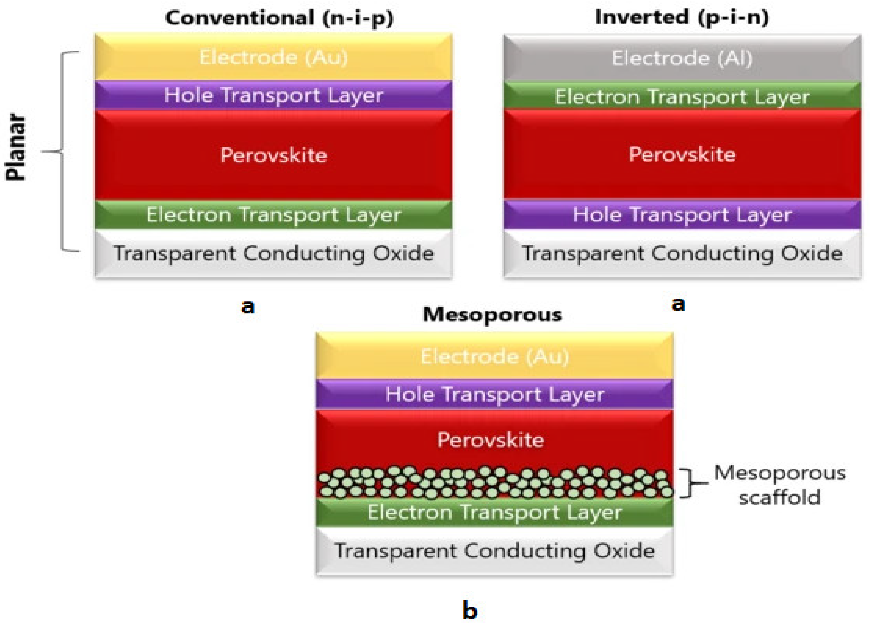
The PSC’s general configuration contains a tin-doped indium oxide (ITO)/fluorine-doped tin oxide (FTO), electron transport layer (ETL), perovskite layer, hole transport layer (HTL) and metal electrode [18]. Usually, PSC consists of two main architectures, mesoporous and planar structures. The mesoporous design enables the light absorption layer to enhance the light-receiving area.
Compared to other solar technologies, different wavelengths of light can affect the PSC performance and as a result, they can convert a proportionately higher amount of sunlight into electricity. Thus, enhancing the material quality of the perovskite-based material increases carriers’ mobility and lifetimes and decreases defect density. Aside from the material quality, reducing the active layer thickness is also a way to implement the above-mentioned electrical benefits. There are two classifications in the planar configuration, conventional n-i-p and inverted p-i-n systems; both are depicted in Figure 1. As Figure 1 signifies, a mesoporous structure comprises an additional layer between the electron transport and perovskite layers. Generally, TiO2 is used as a mesoporous layer, allowing perovskite material to penetrate the pores of the TiO2 solution and, hence, improving the surface area of the perovskite layer.
Additionally, the mesoporous layer supports inhibiting electron-hole pairs’ recombination process and improving the PSC’s PCE [15,19]. As the perovskite material possesses hole-transporting properties, PSC with a hole-transport material-free structure is also possible. A thick perovskite layer with a smooth surface and a reliable back contact is needed to achieve greater efficiency [20]. While the first perovskite solar cell with an HTM-free structure achieved a PCE of 5.5%, it used the TiO2/CH3NH3PbI3/Au configuration in an FTO sheet [21].
The commercialisation of PV technology is influenced by several factors like efficiency, stability and easiness in manufacturing technology. The rapid progress in PSC’s efficiency and stability gained massive attention among researchers and is considered an environmentally and economically viable PV technology. The most pronounced setback of the PSCs is their poor stability in ambient conditions. This setback put a restriction on the robustness of the PSCs. The degradation of perovskite materials in PSC starts from multiple sources [22]. Moisture adsorption and photo-dissociation in the presence of UV light are at the top of the list [23]. Other weak but significant source of degradation includes photo-oxidation, ion migration and light-induced halide segregation. These degradation sources apply to PSC materials and solar cell devices [24]. Besides, some device-only sources of degradation, like metal ion diffusion and mechanical stress, are also there [25]. Even though modern packaging almost eliminates the chance of moisture or oxygen penetration to the solar cell, high-quality packaging can be expensive and bear a high percentage of the total cost of the solar panel [26,27]. In addition, before the final packaging, all solar cells must be transported in an open atmosphere for some time [27]. Therefore, a degree of intrinsic resistance against environmental factors is always required.
However, solar PV development’s central aim is to enhance efficiency and improve manufacturing technology to reduce the overall cost. Furthermore, since the efficiency between the PSC and other commercially available PV modules is comparatively similar, PSC testing for commercial-scale production is essential to enhance solar PV deployment swiftness [28].
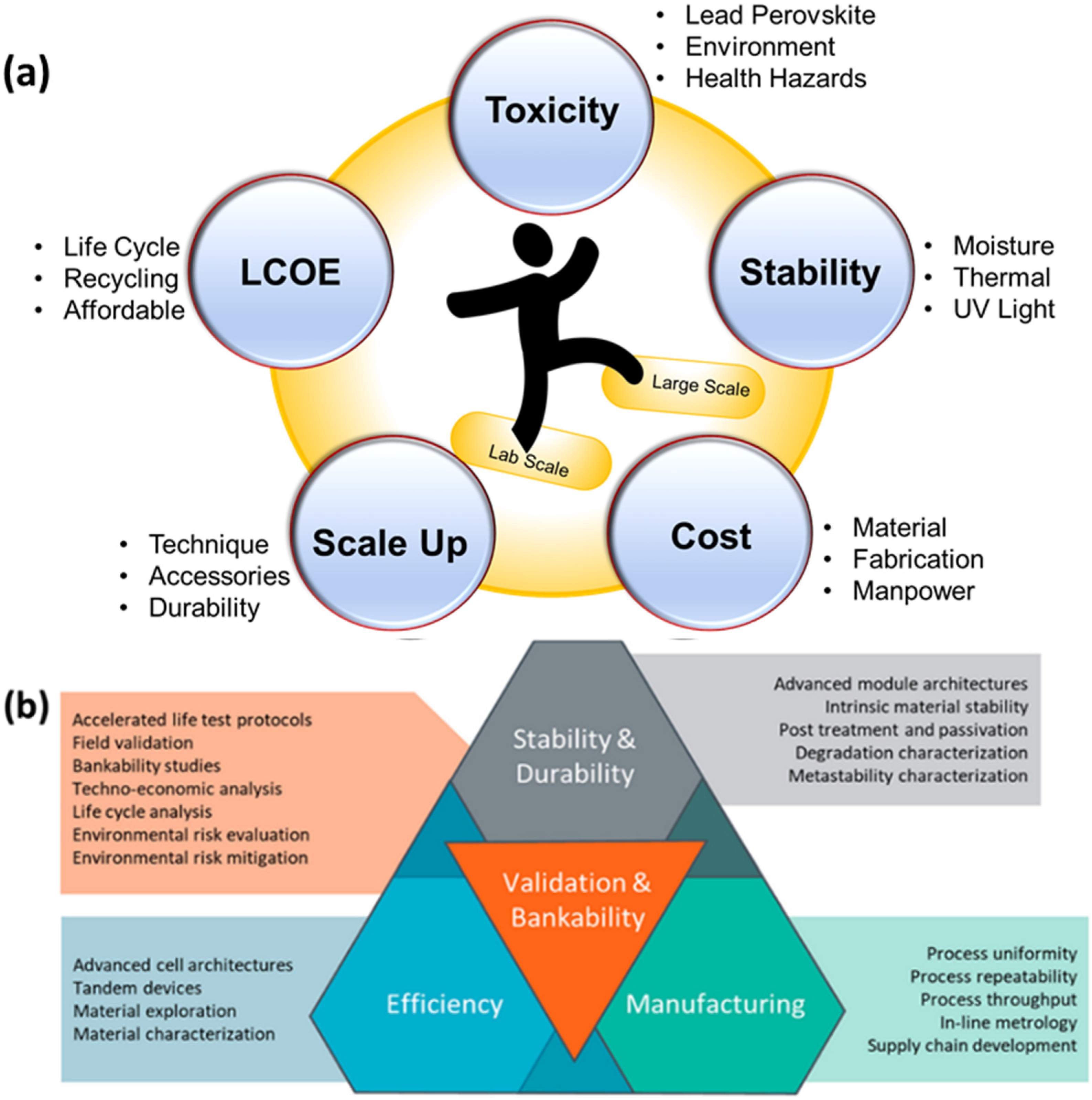
Despite potentially replacing silicon-based solar cells with high device efficiency and low-cost fabrication, PSC also faces significant commercialization challenges (Figure 2a). Considering the rapid PCE revolution, PSC’s scaling up from lab cells to industrial modules is necessary. This can be achieved by lifetimes comparable to legacy PV technologies [28]. The most pronounced setback of the PSCs is their poor stability in ambient conditions. This setback put a restriction on the robustness of the PSCs. The degradation of perovskite material, as well as device, starts from multiple sources [29]. The technological challenge is using the entire solar spectrum with better sensitisers and overcoming the fundamental power-loss mechanism [30].
As the solvents vary due to tolerant evaporation rates at distinct locations, the halide perovskites crystal growth fluctuates. Ion migration can occur during the deposition of precursor solution concentration in the large-area substrate, leading to inhomogeneous crystallisation formation [31]. Often the direct contacts of pinholes in perovskite films initialise the direct contact between the HTL and ETL or other layers can influence the modules’ current leakage and voltage loss. Factors like device hysteresis due to a selection of materials, material toxicity, ambient stability, and costlier and corrosive noble metal electrodes are classified as the significant challenges for PSC commercialization on a wide scale. Moisture adsorption and photo-dissociation in the presence of UV light in PSC are at the top of the list [32]. Other weak but significant degradation sources include photo-oxidation, ion migration and light-induced halide segregation. These sources of degradation apply to PSCs.
Besides, some device-only sources of degradation, like metal ion diffusion and mechanical stress, are also there. Even though modern packaging almost eliminates the chance of moisture or oxygen penetration to the solar cell, high-quality packaging can be expensive and bear a high percentage of the total cost of the solar panel. In addition, before the final packaging, all solar cells must be transported in an open atmosphere [33]. Therefore, a degree of intrinsic resistance against environmental factors is always required. Best encapsulation can be applied to a PSC to keep moisture at bay. However, when it comes to PV material, photostability is the prime demand [34]. Here, the robustness of an encapsulated PSC under light illumination is essential. Halide segregation alters the uniformity of spatial distribution of different halides in the perovskite film. This effect is claimed to be reversible, but in normal operating conditions, the solar cell is under illumination. Changes in halide ions’ redistributive optical band gap affect the PV performance of the cell. Whatever the decomposition route is, the ultimate solid left over is PbI2, the origin of the yellow colour of decomposed MAPbI3. MAPbI3 undergoes quick dissociation in an oxygen environment when light is present. Photo-assisted oxidation of perovskite has two channels of mechanism, namely the first one is the direct diffusion of oxygen molecules into the perovskite lattice through halide-vacancy. The broadband gap oxide type ETM mediates the second channel of oxygen-induced degradation halide in the PSC. UV light can be blocked or, more efficiently, be down-converted visible light, producing photocurrent.
In addition to addressing the concerns regarding mass production and stability, a sophisticated life cycle assessment should be performed, which includes production processes, an evaluation of materials and environmental impact [35,36]. The life cycle assessment of PSCs has also raised concerns about the environmental effects [37]. Other upgrades will need to include recycling methods to address concerns regarding the toxicity of lead, industry-scale electronic-grade films and the adoption of standardised testing protocols to predict the operation lifetime of PSCs [38,39]. Modules must endure degradations due to light, partial or complete shading stress and mechanical shock [40]. The field can learn to form the commercialisation pathway of mature PV technologies as it strives to define and overcomes the hurdles to PSC commercial impact [41]. PSC’s cost analysis depends on various factors like base materials price, cost of labour, factory product yield and the usage of instruments. A significant cost contribution will be for the electrode parts like transparent conductive glasses like fluorine-doped tin oxide (FTO), ETL and HTL materials [42]. Alternatively, researchers must consider the sustainable, affordable preparation of PSCs by employing ETL-free or HTL-free layers and transparent-low-cost conductive oxide glasses. This offers a competitive levelized cost of electricity (LCOE) with the other commercially available PV technologies [43]. The United States Department of Energy Solar Energy Technologies Office’s (SETO) has established a 2030 goal for silicon PV technologies to achieve $0.02 per kWh over the module’s lifetime. For perovskite PV to compete with this, modules will have to last at least 20 years in the field, requiring a significant improvement in long-term stability [44]. In 2020, the global PSCs market held to be USD 352.2 Million and is calculated to gain at least USD 2012.7 Million by 2027 [45]. The market is anticipated to register a CAGR of 28.7% during the forecast period. The LCOE of the commercial perovskite PV modules requires evidence of the system’s reliability and a holistic approach (Figure 2b) [46].
Figure 2.
A schematic illustration of (a) factors in upscaling the manufacture of PSC devices and (b) technical challenges for commercializing PSCs [46].
Figure 2.
A schematic illustration of (a) factors in upscaling the manufacture of PSC devices and (b) technical challenges for commercializing PSCs [46].

Timeline of PSC Progression
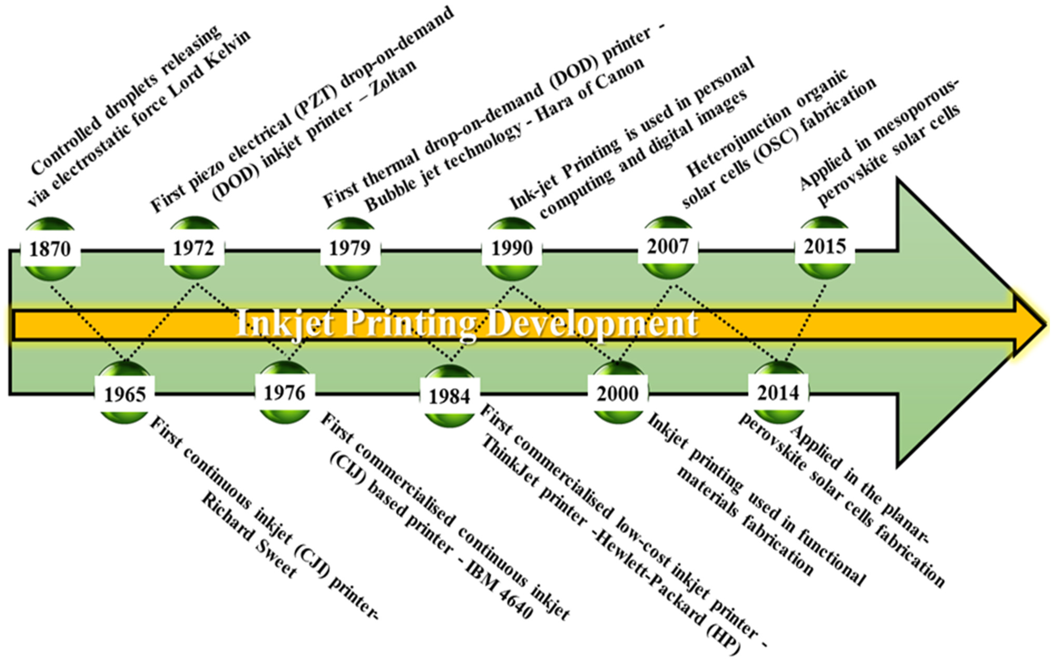
In 2009, The perovskite structured material was first used as a replacement for dye pigment in dye-sensitised solar cells, achieving a PCE of 1.81% [7]. Nevertheless, the low efficiency and poor stability due to the liquid electrolyte-based hole transport layer diminished the significance of the breakthrough [8]. In 2012, perovskite nanocrystals were used as a light absorber for solid-state mesoscopic solar cells, and they obtained an efficiency of 9.7% [9]. Instead of using the liquid electrolyte technique, they used 2,2′,7,7′-Tetrakis[N,N-di(4-methoxyphenyl)amino]-9,9′-spirobifluorene (Spiro-MeOTAD) as the hole transport layer and mesoporous-TiO2 as electron transport material [8]. After that, perovskite solar cells attracted wide attention from worldwide researchers. Table 1 illustrates the efficiency improvements of PSC over the last decade. In 2020, Nishigaki et al. demonstrated a simulation study that implies a maximum of 38.7% PCE for crystalline Si/perovskite tandem structure [19]. However, the PSC performance improvements have been carried out through various device architecture modifications, such as adding a new version of carrier transport materials (HTLs and ETLs) and enhancing the absorber layer. Apart from these properties, the film deposition technique handles a significant role in the formation of the PSC performance.
2. PSC—Fabrication Techniques
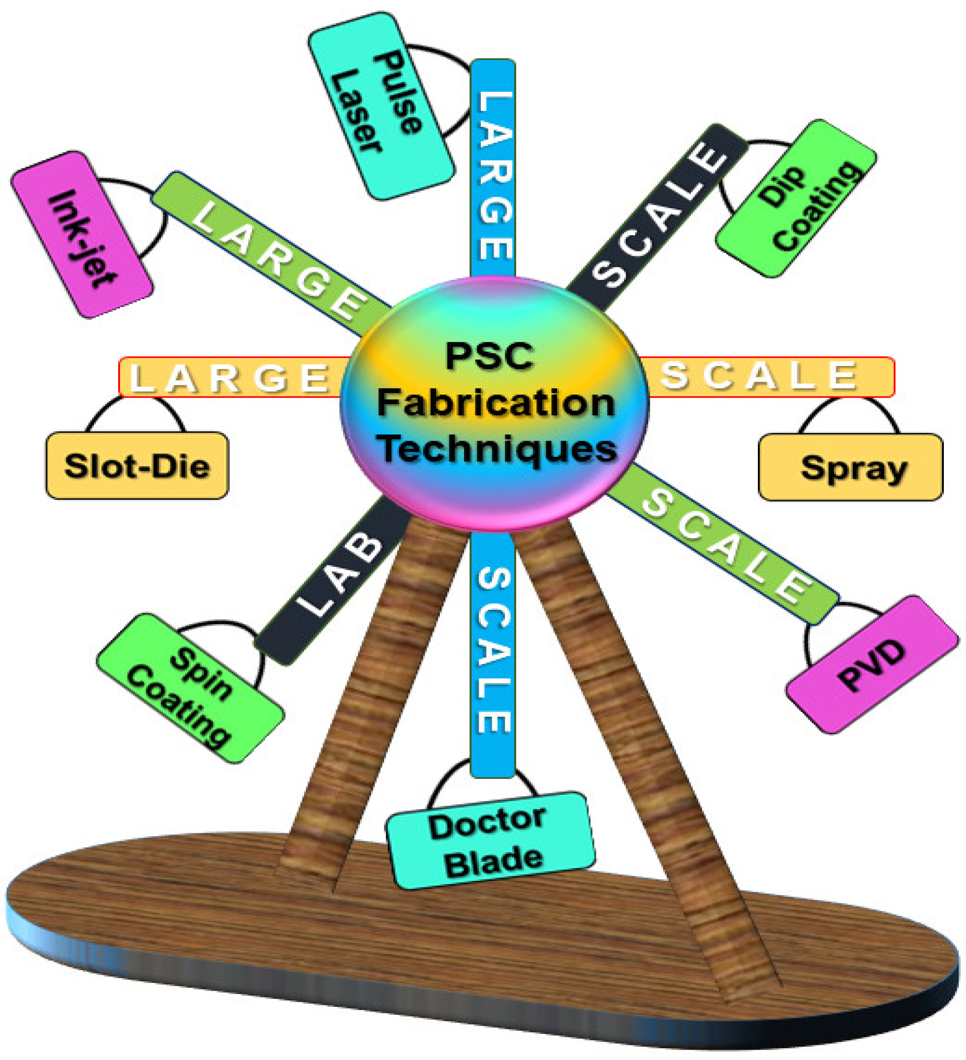
PSCs are a leading force in the area of photovoltaic. Explored theories are streaming regarding the fabrication and analysis of the high-efficient PSC and its layer material. Long-term stability and PCE are two significant parameters for applying PSCs in the industry. Many manufacturing techniques have been tested and documented for PSCs, including spray coating, drop-casting, ultrasonic spray coating, electrodeposition, slot-die coating, chemical vapour deposition, thermal vapour deposition, vacuum deposition, screen printing, inkjet printing, etc., with various product architectures. Figure 3 mentions the classification of PSC deposition techniques and the lab-based and large-scale fabrication methods.
One of the critical parameters in determining the PSC performance is the quality of the layers, yet various fabrication techniques have been established to enhance the PSC layers’ quality. Among researchers, the most well-known method for PSC fabrication is spin coating. Nevertheless, it suffers from issues like scalability and poor reproducibility. However, the rapidly mounting community of researchers is widely investigating several scalable deposition techniques such as inkjet printing, slot-die coating, spray coating, blade coating, etc. Generally, we can categorize the printing technologies into lab-scale and large-scale processes; Table 2 indicates the coating technology’s classification and properties.
2.1. Slot-Die Coating
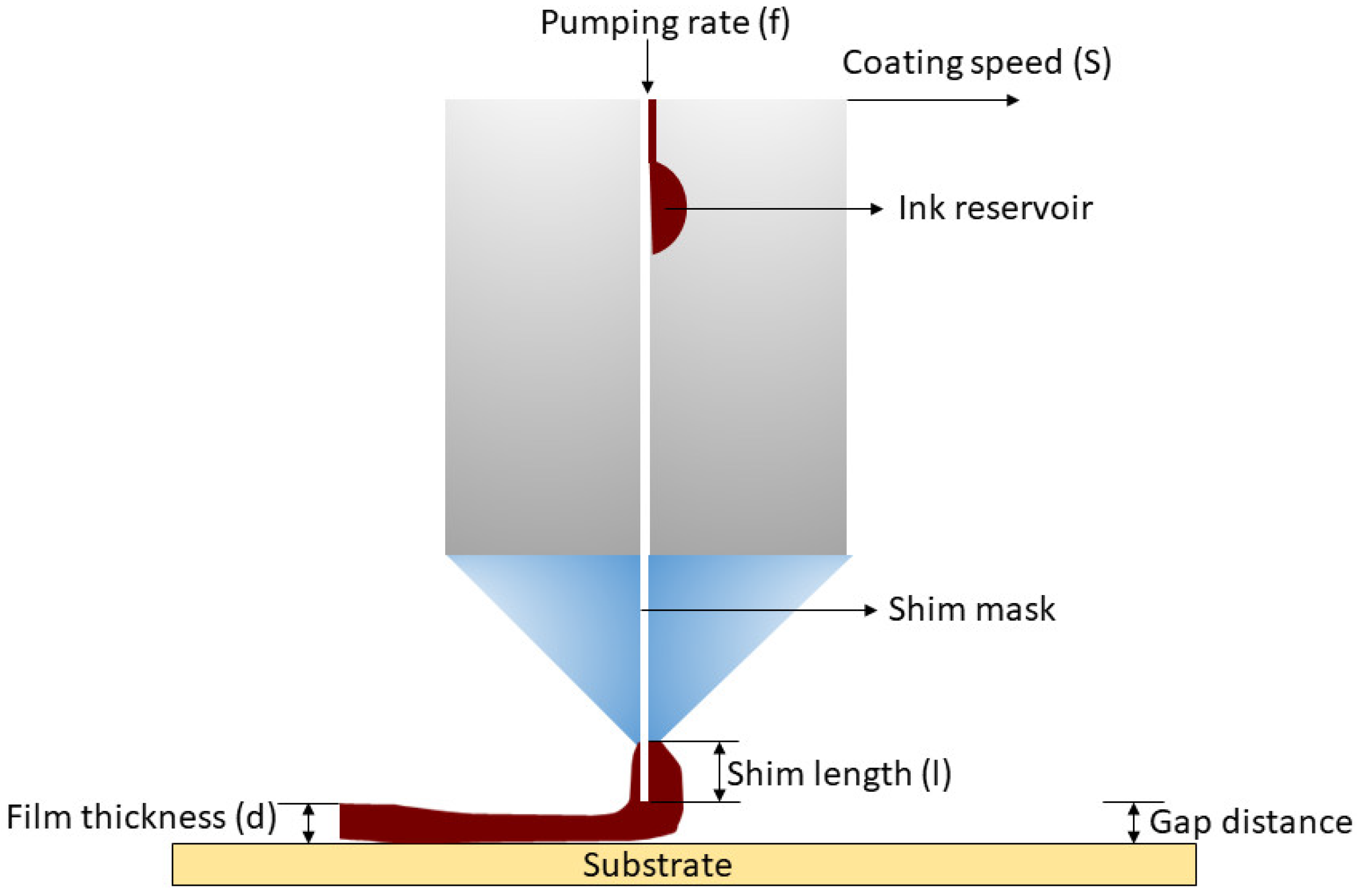
Slot-die coating is widely used and well suited for deposition perovskite and other PSCs perovskite solar cell coating layers. This technology is classified as a pre-metered coating technique and a highly scalable technology, enabling uniform thin film coating with low operational cost and minimal material waste [55]. As shown in Figure 4, a standard slot-die coating mechanism includes an ink reservoir, coating head or slot-die head positioned towards the substrate, and through a syringe pump, the prepared ink is forced into the coating head [55]. Afterwards, the ink will come out of a narrow slit in the coating head, creating a liquid bridge between the substrate and slot-die head [55]. When the substrate moves across the coating head, deposition happens, and the layer thickness is controlled by varying the slit size of the coating head and the moving speed of the substrate [55]. The fluid rheological property can also impact the wet and dry film thickness.
The slot-die coating has some common problems like breakup, air-infiltration and the effect of fluid properties. Split in the downstream meniscus causes a discontinuity in the layer. Furthermore, the miscalculation of the low-flow limit facilitates the separation. The low-flow limit is the minimum thickness coated at a given substrate speed [56,57]. During the low-flow limit calculation, the fluid’s parameters, like viscosity, capillary action and inertial forces, were measured [56]. Air infiltration in the upstream meniscus can lead to the creation of bubbles in the wet film. Additionally, this can create defects like rivulets and multiple smaller stripes with gaps [55]. As indicated in Figure 4, the critical parameters during the slot-die coating are the gap distance, coating speed, and pumping rate. Perovskite film coating by slot-die printing is classified into one- or two-step coating methods. The one-step method, also known as the single-step method, provides better control over the final perovskite compositions than the two-step. Compared to the two-step coating, the one -step method has the advantages of low solvent wastage and a faster and simplified process. One disadvantage of the one-step method is the potential rapid crystallisation of material upon deposition resulting in the complex crystallisation control.
In 2021, Yang et al. used slot-die coating and additive method and an area of 20.77 cm2 PSC was fabricated with a certified quasi-stabilised efficiency of 16.63% [56]. Additionally, in the same year, Xu et al. adapted the infiltration technique into the slot-die coating mechanism, produced triple mesoscopic perovskite solar mini modules with an active area of 60.08 cm2 and showed an efficiency of 12.87% [57].
Burkitt et al. used slot-die coating to fabricate all four layers of PSC (n-i-p structure) and achieved an efficiency of 7% [58]. In this process, TiO2 is used as the mesoporous scaffold layer, CH3NH3PbICl2 as the perovskite layer and the spiro-MeOTAD hole-transport layer [58]. The slot-die-coated films were deposited at 1.0 m/min with an ink flow rate (pump rate) of 0.5 mL/min for the perovskite layer [58]. Subsequently, the coated films were placed in a coating machine’s in-line oven at 105 °C by giving an oven residence time of 3 min, then dried in a fan oven at 100 °C for 90 min [58]. The mesoporous TiO2 layer was deposited at a 0.1 m/min coating speed with a 0.05 mL/min pump rate and obtained 10 μm wet film thickness. Afterwards, it undergoes a heating process of 10 min at 140 °C and another 30 min at 550 °C [58]. The hole transport layer was deposited at a 1.0 m/min coating speed with a 0.5 mL/min pump rate. Later, the material was left for overnight drying (around 16 h) at room temperature and placed in a box with desiccants to reduce humidity and enhance the films’ oxidation [58].
Schmidt et al. fabricated a PSC with a one-step coating of DMF solution containing PbCl2 and MAI and achieved an efficiency of 4.9% [59]. They found that the spin-coated device’s low efficiency is the primary reason for its low efficiency, the inferior quality of a flexible polyethene terephthalate ITO substrate and the perovskite films’ morphology [59]. Cotella et al. used a one-step deposition of mixed lead halide perovskite on a preheated substrate and an air knife-blow drying technology to improve the film morphology with crystallisation [60]. They found that surface roughness was reduced due to the drying process enhancement, and the surface coverage increased, gaining a PCE of 9.2% [60]. Similarly, Kim et al. fabricated PSC with planar n-i-p structure (ITO/ZnO/MAPbI3/HTM/MoO3/Ag) using blow-drying N2 gas to acquire better morphology of the perovskite film and achieved an efficiency of 12.7% [61].
Verhees et al. fabricated a perovskite PV module with an area of 12.5 × 13.5 cm2, and they used a scalable sheet-to-sheet slot die coating method and the laser ablation process. For the experiment, perovskite solar cells with planar n-i-p architecture (Glass/ITO/c-TiO2/CH3NH3PbI3−xCl/Spiro-OMeTAD/Au) were used and achieved a PCE of 10% [62]. The NH4Cl addition to the perovskite layer enhances the perovskite film’s crystallinity and morphology [63]. Zuo et al. found that the inclusion of NH4Cl into the precursor solution improved the slot-die-coated perovskite film morphology [64]. Moreover, blow-drying using N2 has been used for annealing and received an efficiency of 15.57% [64]. The N2 blow-drying process is widely used in the two-step and one-step coating methods to produce uniform coating and controlled crystallinity for the slot-die-coated device. While the blow-drying process needs a controlled flow of gas and an optimised location, Kim et al. reported that device performance’s reproducibility is complex [65,66]. M. Xu et al. recently demonstrated the slot-die coating process of a novel precursor ink for an efficient triple-mesoscopic solar mini-module with a PCE of 13% for an active area of 60.08 cm2 [67].
2.2. Inkjet Printing Technology
Inkjet printing is famous for printing images or computer data into a porous surface, and this technology is considered a material-conserving deposition method for liquid-state materials [68]. Until 2000, inkjet printing was used to print digital images or data from a computer to a porous surface. In 2014, researchers started using inkjet printing technology to fabricate the PSC. However, they started to print the functional material; in 2007, the first heterojunction organic solar cell was fabricated through inkjet printing. In 2021, Li et al. developed a new ink system which has n-methyl pyrrolidone (NMP) and dimethylformamide (DMF) as solvents [69]. The NMP solvent can adjust the viscosity, which influences the precursor solution’s surface energy; this ink developed a device of 4.00 cm2 area with a PCE of 14.5% [69]. The basic operating principle involves the ejection of a fixed quantity of ink through a nozzle, carried out by piezoelectric action [68]. When the external voltage is applied to the chamber filled with ink, a quasi-adiabatic reduction will occur, and the nozzle ejects the ink into droplets [68]. The ejected drop will be under the influence of both gravity and air resistance.
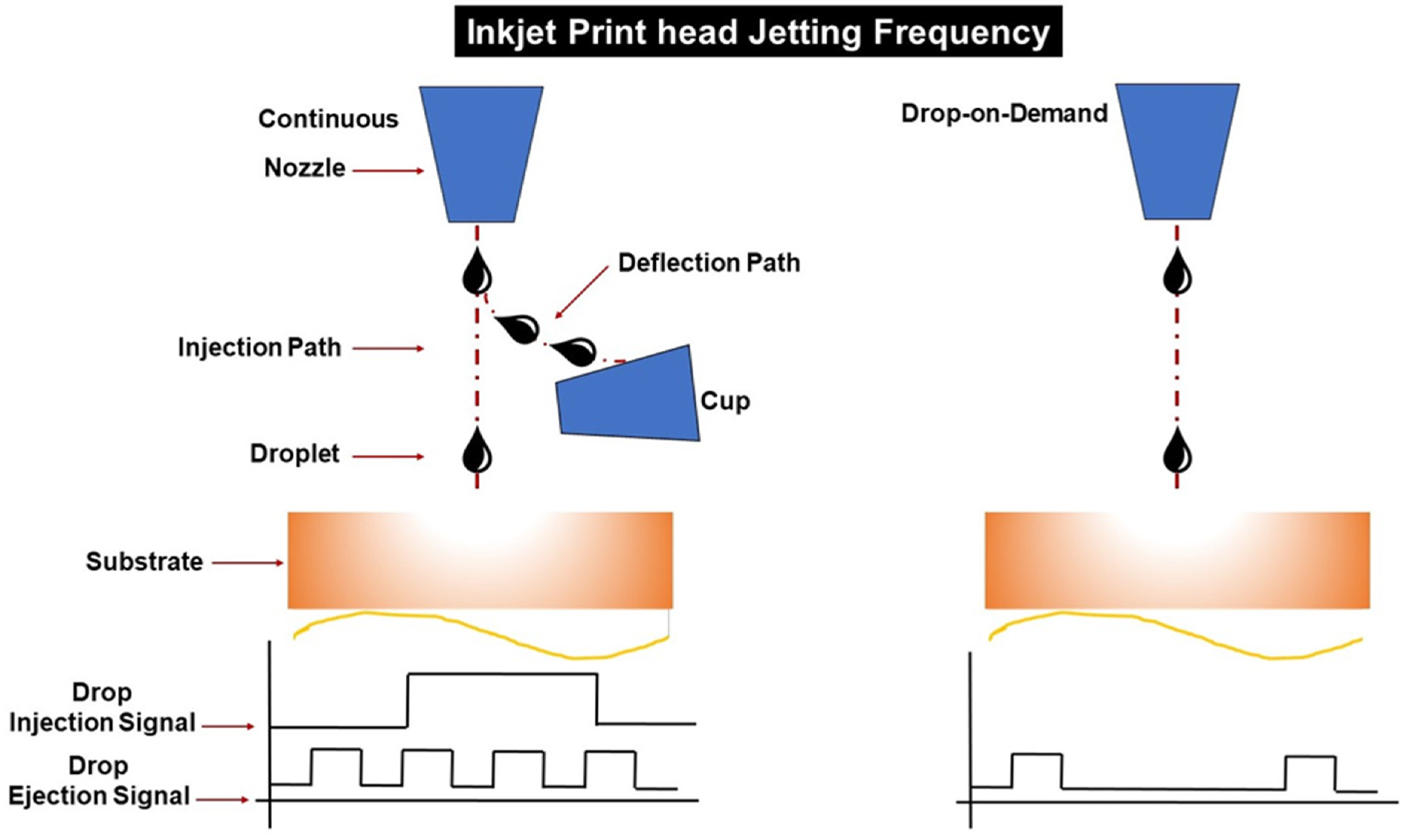
The rapid ink-jet printing process can transform lab-scale devices into large-scale ones. Panasonic demonstrated a large-area perovskite module using the ink-jet printing method and showed an efficiency of 16.09%. They used ink-jet printing for depositing all the layers, including the perovskite layer. The key advantages of inkjet printing are that it provides flexibility in thickness and shape and is considered a material-efficient technology. Moreover, ink viscosity, contact angle, surface tension and momentum influence ink spreading [70,71]. As illustrated in Figure 5, inkjet printing technology is classified into two, continuous and drop-on-demand (DoD) inkjet printing [72]. In the constant inkjet printing technology, a steady voltage supply is provided throughout the operation, and in the drop-on-demand type, the voltage is supplied as per the demand [72].
On the other hand, the crystallisation control through the anti-solvent application techniques is limited, and the printing speed is comparatively slower for PSC fabrication. This enhances the complexity of the upscaling process as well. Considering the significant parameters, it will be similar to the slot-die coating method, the gap distance, coating speed, the rheological characteristics of the inks and the pumping rate.
X. Peng et al. applied the technology in manufacturing mesoporous-perovskite solar cells. Z. Wei et al. reported the first inkjet printing of planar-perovskite solar cells in 2014, achieving a PCE of 11.60% [73]. In this process, ink consists of carbon and methyl ammonium diode (MAI) coated on the PbI2 layer. After one hour of annealing, the photoactive MAPbI3 layer formed due to the PbI2 layer conversion [73]. Moreover, in 2015, the first mesoporous-perovskite solar cells were fabricated through inkjet printing. They also investigated the importance of printing table temperature by conducting experiments at different temperatures like 25, 40, 50 and 60 ℃ [74]. After analysing the results, the printing table with 50 ℃ is suitable for forming large crystals with a high surface area and received a PCE of 7.9% [74]. The ink used in the process was constituted by mixing MAI and PbI2 in γ-butyrolactone [74].
Furthermore, in 2017, hole transport layer-free mesoporous PSC was fabricated through inkjet printing [75]. The device comprised glass/FTO/TiO2/ZrO2/MAPbI3/Carbon, and the precursor ink was a mixture of PbI2 and MAI with 5-AVAI, ammonium valeric acid iodide [75]. The ammonium valeric acid iodide acts as an emplacing agent and improves the crystalline property and the charge-carrier lifetime of MAPBI3 [75]. The perovskite solar cell achieved a PCE of 7.83% during the forward bias scan and 8.74% on the reverse bias scan [75]. While the ink properties play an essential role in determining the fabricated solar cell performance, the fluid dynamics calculation of ink is crucial. While the ink properties play an indispensable role in determining the fabricated solar cell performance, the fluid dynamics calculation of ink is vital. The rocket ride of the PSC efficiency in comparison to other new-generation PVs is shown in Figure 6. This improvement is so huge in such a small timeframe that it has attracted tremendous research for renewable energy research for cheap yet excellent solar cells.
2.3. Spin Coating
Spin coating is a technique that deposits the film by dispensing the solution into a platform which rotates or begins to rotate. The centripetal force created during the rotation spreads the material, and the thickness is controlled by adjusting the rotational speed [76]. The steps involved in the spin coating process are spin-up, deposition, spin-off and evaporation. During the spin-up process, the substrate reaches the desired rotation speed, and then the solution drops into the substrate using a pipette. In this stage, the fluid and the substrate’s spinning rate differ and expel out from the substrate [76], while both will match up when the rotational acceleration matchup up with the drag of the solution. The duration of the rotation changes according to the required thickness. After that, the spin-off’s rotational speed is reduced, and the process stops. Then, the coated material is placed on the hot plate for evaporation and annealing. The factors like pressure, external conditions and volatility of the solvent can influence the evaporation rate. Even some high viscous fluid nature can affect the evaporation rate factors, leading to the buildup of solvent on the substrate.
Spin coating is widely used in perovskite solar cell fabrication because of its low-material requirement and simplicity. However, this is not scalable and can only be used for lab-based research. However, one-step spin coating and two-step spin coating are two approaches for depositing perovskite solution. Figure 7a indicates the one-step coating, and Figure 7b implies the two-step coating. To deposit (MAPbI3) solution onto the substrate through a one-step coating method, both the MAI and PbI2 are mixed in solvent dimethylformamide (DMF) or dimethyl sulfoxide (DMSO), and this solution is dropped over the substrate for the spin coating [19]. For depositing perovskite solution (MAPbI3) through a two-step spin coating, the PbI2 key is dropped onto the spinning substrate to create a PbI2 film [19]. Afterwards, a 2-propanol solution of MA+ was released on the film. The coating parameters like spinning rate, temperature, time and viscosity of the solution have a role in the PSC performance. Studies show that two-step coating produces a cuboid-like crystal morphology [77]. These techniques coat other layers like hole transport and electron transport layers of PSC. A considerable amount of PSC lab fabrication is carried out through the spin coating.
2.4. Thermal Evaporation
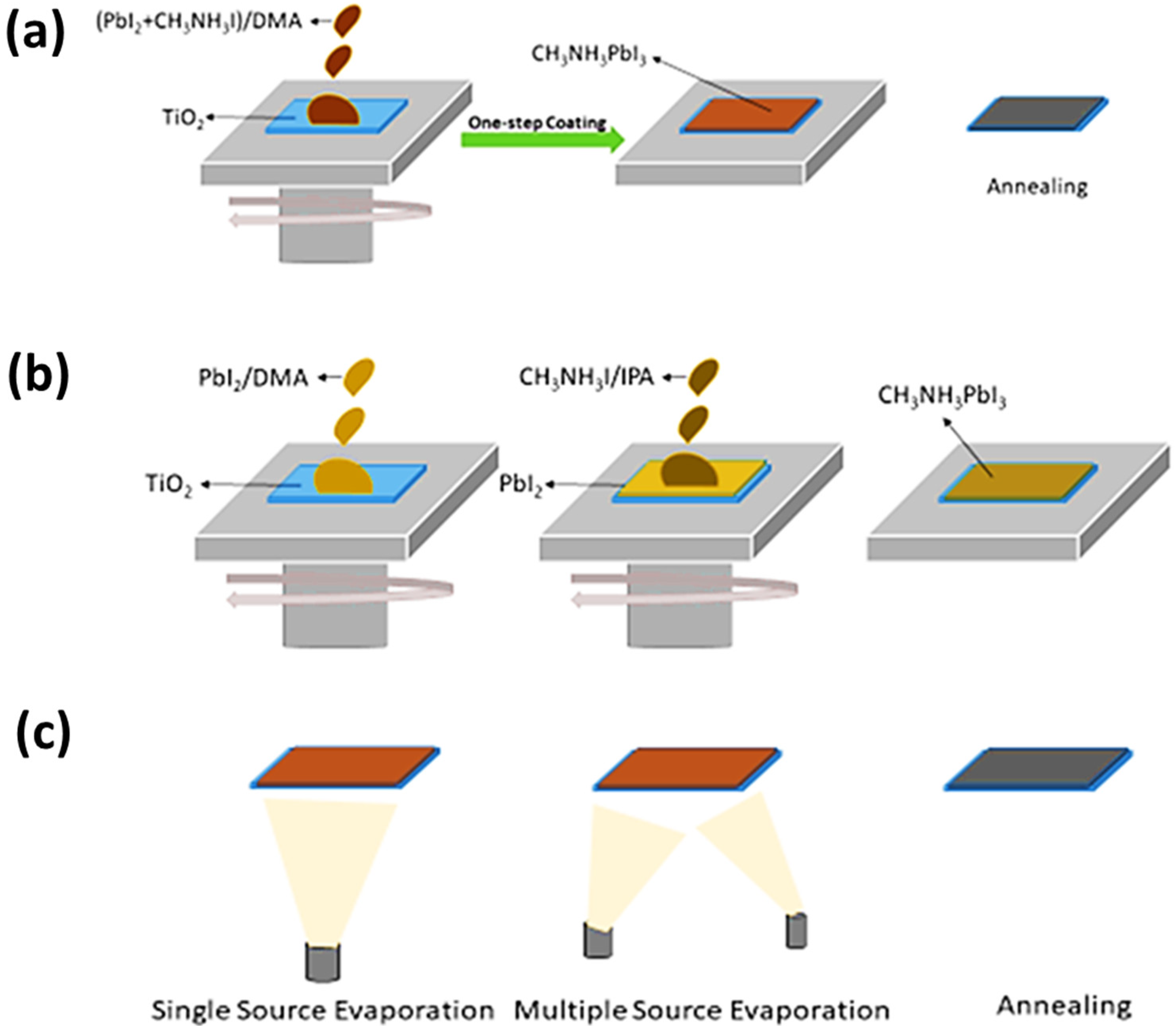
In this technique, perovskite films are prepared through the thermal evaporation of chemicals and are generally carried out in high-vacuum conditions [15]. Figure 7c shows that the thermal evaporation method is classified into single and multiple-source evaporations. The perovskite absorber is deposited into the ceramic crucibles and placed in the nitrogen-filled glove box to begin the process during the coating process. Subsequently, MAX and PbI2 were deposited on the FTO-coated glass with a TiO2 layer [78]. While the method requires a high temperature to evaporate PbI2, this makes the process complex and potentially releases toxic gases. Additionally, MAPbI3 coating in the planar heterojunction PSC were reported through dual-source evaporation and achieved a PCE of 15.7% [78]. Figure 3 indicates that this method is used for lab and large-scale PSC fabrication.
Afterwards, to overcome the drawbacks vapour-deposition method, the vapour-assisted solution method was introduced. PbX2 was deposited into the TiO2-covered FTO-coated glass through the solution method. Due to the MAX vapour reaction at 120–165 °C in a nitrogen atmosphere for 2–4 h, MAPbX3 grains will be developed [74]. Nevertheless, the incomplete response of PbX2 films bottom with MAX vapour decreases the cell’s power output due to the enhancement of internal resistance [71]. Therefore, perovskite cells with sequential vapour deposition have achieved a power conversion efficiency of 15.4% [73] in 2020. Lei et al. fabricated an all-evaporation processable PSC with an active area of 16 cm2 and obtained an efficiency of 13% [79]. Additionally, recent development for vacuum-processed flexible perovskite solar modules demonstrated a PCE of 14% [80]. These results from the thermal evaporation techniques implicate the potential of PSC’s scale-up.
2.5. Spray Coating
Spray coating is a solution-based deposition technique used in the automotive painting industry. The roll-roll compatibility drew the scientific community’s attention to use this technology for PSC fabrication. The printing setup for the PSC fabrication consists of atomising and deposition systems connected to the quartz nozzle, enabling the perovskite precursor solution addition. The atomiser initiates the conversion of the precursor solution into tiny droplets [81]. Afterwards, low-pressure gas streams direct the droplets into the substrate, and the deposition system enables solvent evaporation and the perovskite film deposited on the substrate. The perovskite film’s quality over the substrate was determined by examining the characteristics of precursor liquid droplets. Accumulation of perovskite solution due to the surface tension can lead to low wettability. The liquid injection rate over the spray coating head determines the film thickness. Concerning the coating speed, the meniscus coatings are classified into two low-speed and Landau-Levich regimes. The Landau-Levich regime has a higher coating speed, and the evaporation regime has a lower coating speed. However, increasing the solvent evaporation rate by keeping the substrate high reduces the irregularities [82]. Barrow et al. used ultrasonic spraying to print perovskite and the ETL layers for the first time and attained a PCE of 11% [83]. Even though the spray coating’s experimental arrangement is identical to inkjet printing, the spray coating has been classified into ultrasonic spraying, pneumatic spraying and electrospraying. The classification is based on droplet dispersion over the substrate [81]. In addition, Table 3 depicts the newly fabricated stable perovskite devices and shows the usage of spray coating.
The Electrospray-assisted deposition technique involves depositing any layers in the perovskite solar cells. It is carried out by pumping the solution through a capillary needle at a higher voltage. Kavadiya et al. validated this technique by depositing MAI over the PbI2 layer and achieved an efficiency of 12%, with 4000 h of stability [84]. The film formation reaction has controlled, enhanced strength and facilitated a highly stable-moisture-resistant perovskite layer [84]. A substrate-to-needle distance and the solution’s flow rate have a crucial role in shaping the perovskite layer throughout the process.
Additionally, they demonstrated the self-healing capability of the layer in the stability test. Water vapour was sprayed over the coated film until it degraded to PbI2 and heated at 100 °C. Then, they observed that the PbI2 layer reverted to perovskite and the film colour changed from yellow to dark brown [84]. Before and after the water exposure, the film showed similar XRD spectra [84].
In 2017, this technology used electro-sprayed CuxO as the hole transport layer and attained an efficiency of 5.8% [85]. They found that the electro-sprayed layer’s excessive thickness leads to the solar cell’s degradation due to the enhanced light absorption and series resistance [85]. Simultaneously, low surface coverage due to insufficient thickness reduces the cell’s performance [85]. However, this technique is considered scalable and losses are minimal due to the material deposition quantity control. Even though this technology is not widely used for perovskite fabrication, the electrospray-assisted technique is promising for PSC’s commercial making.
2.6. Screen Printing
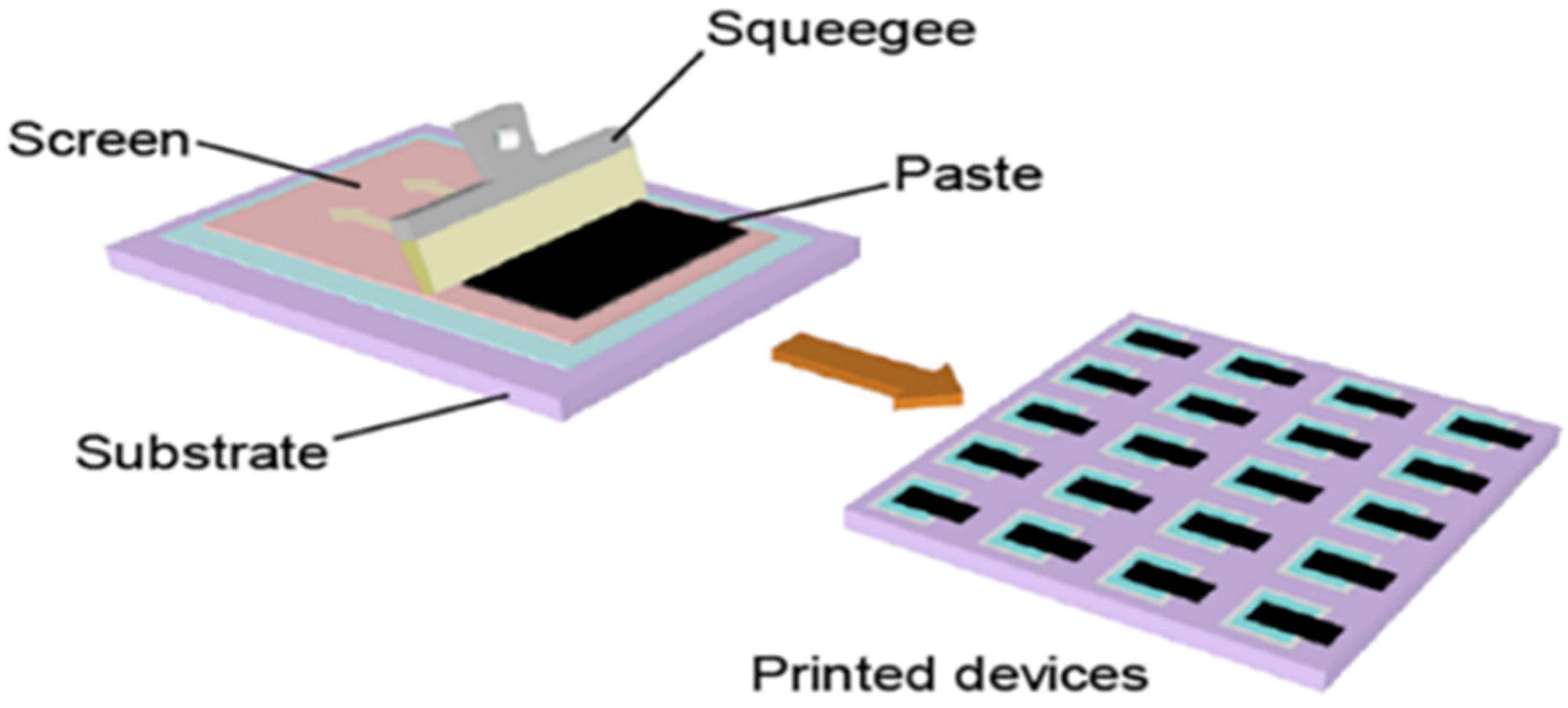
The screen-printing technique is classified based on printing platform, flat-bed screen printing and rotary screen printing [82]. Screen printing is widely used to manufacture traditional silicon solar cells and PSCs. It can produce a sizeable wet film thickness and requires low volatility and a high-viscosity coating solution. At first, this technique was widely used in making dye-sensitised solar cells with a large area and then applied in PSC fabrication [86,87]
Emulsion application into the spaces makes provisions for printing patterns. Usually, screen printers have a screen of woven material like synthetic fibre or steel mesh and are glued to a frame under tension; Figure 8 indicates the screen-printing technique. After that, the squeegee moved over the screen, packed with the coating solution. The squeegee movement in the screen printer helps coat the material at emulsion-free paces. The printed layers’ wet thickness depends on the volume between threads of the emulsion’s mask and thickness [87]. Additionally, the variation of the screen’s tensions, ink properties and squeegee velocity affect the reproducibility.
The screen-printing technique facilitates the solution’s deposition up to several square meters and the material utilisation is comparatively higher for the continuous process. However, screen printing consumes low material during small-scale applications and provides low-cost PSC testing. Priyadarshi et al. reported a fully screen-printed mesoporous PSC with an active area of 70 cm2 and achieved a PCE of 10.74% [88]. A screen-printed module with an active area of 198 m2 was fabricated and delivered a PCE of 5% [89]. After storing the perovskite module in the dark at ambient conditions, the efficiency increased to 6.6% [89]. Considering the stability of the PSC with this printing technique, Table 4 mentiones the stability advancement with different architecture.
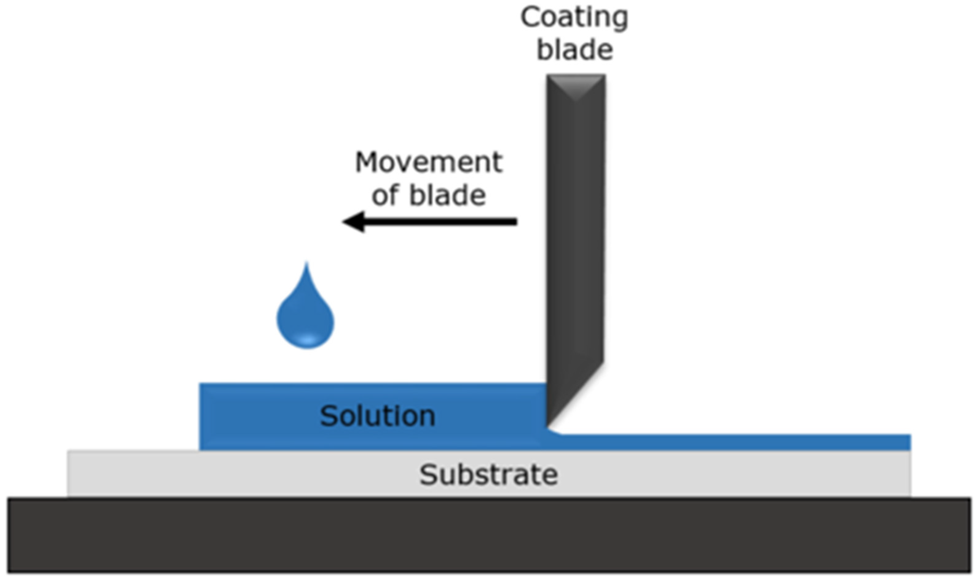
2.7. Blade Coating
This technique is relatively simple and a scalable fabrication method for perovskite films. The critical tool involved in the coating process is the doctor blade or knife, also known as doctor blading or knife coating [90]. The precursor solution is applied between the coating head and substrate; then, it is coated over a preheated substrate by moving the blade or knife across the substrate. Furthermore, the perovskite film obtained after the solvent evaporation, this technique can cover PSCs with an area of more than 10 cm2. Figure 9 represents the blade coating method. The operation principle resembles the screen-printing approach [91]. However, the controllable substrate temperature can impact the quality of the perovskite film. Table 2 clearly explains the characteristics of blade coating and how blade thickness and coating speed play a vital role in determining the film’s efficiency [92,93].
Huang et al. introduced perovskite ink to enhance perovskite films’ quality at higher coating speeds or Landau-Levich mode [94]. Using L-α-phosphatidylcholine enhanced the film’s adhesion to the hydrophobic substrates and reduced the drying process’s solution flow dynamics [94]. They obtained a stabilised efficiency of 15.3% and 14.6% for devices with an active area of 33 cm2 and 57.2 cm2, respectively, at a coating speed of 180 mh−1 [94]. However, the coating of uniform large-area perovskite films is rugged at a higher rate, so they side-stepped the problem by adding surfactant additives. Also Table 5 reports the PSC advancements with different architectures and how other coating techniques are used.
Figure 9.
Schematic representation of blade coating printing technique [95].
Figure 9.
Schematic representation of blade coating printing technique [95].


Table 3.
Developments in the large area PSC fabrication.
| Cell Area (cm2) | Sub Cells | Printing Method | Configuration | Voc (V) | Jsc (mA cm−2) | FF (%) | PCE (%) | Ref. |
|---|---|---|---|---|---|---|---|---|
| 168.75 | 25 | Slot-die Coating (One-step) | Glass/ITO/TiO2/MAPbI3−xCl/Spiro-OMeTAD/Au | 21.02 (0.848 per cell) | 17.3 | 67.9 | 11.1 | [62] |
| 149.5 | 23 | Slot-die Coating (One-step) | Glass/ITO/TiO2/MAPbI3−xCl/Spiro-OMeTAD/Au | 20.8 (0.904 per cell) | 19 | 70.6 | 11.2 | [62] |
| 16 | _ | Spray Coating | FTO/bl-TiO2/m-TiO2/(HC(NH2)2PbI3)0.85 (CH3NH3PbBr3)0.15/spiro-OMeTAD/Au | 1.13 | 17.3 | 61.9 | 12.1 | [83] |
| 10 | 4 | Slot-die Coating (One-step) | Glass/ITO/PEDOT:PSS/MAPbI3/C60/PCBM/BCP/Ag | 3.8 | 4.1 | 52 | 8.3 | [96] |
ITO: Indium tin oxide, PCBM: Phenyl-C61-butyric acid methyl ester, BCP: Biphasic Calcium Phosphate.
Table 4.
Advancements in the stability of PSC.
| Device Structure | Perovskite Material | Dimensionality | PCE (%) | Stability | References |
|---|---|---|---|---|---|
| FTO/c-TiO2/m-TiO2/perovskite/spiro-OMeTAD/Au | (HOOC(CH2)4NH3)2PbI4/CH3NH3PbI3) | 2D/3D | 14.6 | Zero loss in efficiency for 10,000 h | [21] |
| FTO/mp-TiO2/perovskite/4,4-dimethoxytriphenylamine/Au | (FAPbI3)0.85 (MAPbBr3)0.15 | 3D | 19.17 | 600 h of stability under 40% relative humidity | [97] |
| FTO/mp-TiO2/perovskite/DM/Au | (FAPbI3)0.95 (MAPbBr3)0.05 | 3D | 21.7 | 95% stable after 500 h | [98] |
| FTO/TiO2/perovskite/spiro-OMeTAD/Au | MA2PbI4 | 2D | 16.6 | 97.8% stable after 1512 h with a relative humidity of 55% | [99] |
| FTO/TiO2/perovskite/spiro-OMeTAD/Au | (PDA)(MA)3Pb4I13 | 2D | 13.3 | 95% stable for 4000 h with 40–70% relative humidity | [100] |
| FTO/c-TiO2/m-TiO2/perovskite/spiro-OMeTAD/Au | (Cs0.1FA0.9)Pb(I0.9Br0.1)3 | 2D/3D | 20.8 | 92% stable after 2400 h with 55% relative humidity | [101] |
| FTO/Sn O2/perovskite/spiro-OMeTAD/Au | Cs0.05(FA0.83MA0.17)0.95 Pb(I0.83Br0.17)3 | 2D/3D | 21.06 | 90% stable after 3000 h in the air | [102] |
2D = two-dimension; 3D = three-dimension.
Table 5.
Recently reported perovskite solar cell device designs with different techniques for the layers.
Table 5.
Recently reported perovskite solar cell device designs with different techniques for the layers.
| Perovskite | ETL | HTL | Structure | Architecture | Contacts | Precursor Ink | Area (Active Area cm2) | PCE (%) | Substrate | Year | Ref. |
|---|---|---|---|---|---|---|---|---|---|---|---|
| Solution-bathing | Spin-coating | Spin-coating | Single-cell | p-i-n | Gold | Mixed solvent: DMF/ DMSO, 4/1, v/v) FAI (1.09 M), PbI2 (1.15 M), MABr (0.14 M), PbBr2 (0.20 M) and CsI (0.06 M) | 5 × 5 (1.00) | 18 | ITO-glass | 2020 | [103] |
| Spin-assisted solvent extraction | Spin-coating | Spin-coating | Modules | n-i-p | Silver | Equal-amount of MAI and PbI2 dissolved in 2-pyrrolidinone to make a precursor solution with a concentration of 1.5 M | 10 × 10 (25.2) | 14.36 | ITO-glass | 2020 | [104] |
| Slot-die coating | Slot-die coating | Slot-die coating | Single-cell/module | p-i-n | Silver | Mixed solvent: GBL and DMSO: 96 mg MAI, 276 mg PbI2 and 0.18 mg PEG | 2 2 (0.09; cut from 12 12)/4 4(3.78) | 11/10.34 | FTO-glass | 2020 | [105] |
| Slot-die coating | Slot-die coating | Slot-die coating | Modules | n-i-p | Chromium/Gold | A mix of 15.6 mg CsI and 553.2 mg PbI2 dissolved in 0.9 mL DMF and 0.1 mL DMSO; 2.5 mg FACl and 75 mg FAI dissolved in 1 mL isopropanol | 8 × 8 (35.80) | 15.3 | FTO-glass | 2021 | [106] |
| Spin coating | Chemical bath deposition | Thermal evaporation method | Modules | n-i-p | Gold | A mix of 0.0675 M CsI and 1.35 M PbI2, dissolved in a mixed solution (1.9 mL DMF and 0.1 mL DMSO); FAI 1000 mg; MAI 110 g; MABr 110 mg; MACl 110 mg, dissolved in 15 mL IPA | 10 × 10 (91.8) | 21.70 | FTO-glass | 2021 | [107] |
| Spin coating | Spin-coating | Spin-coating | Modules | n-i-p | Au | A mix of 28 mg CsI and 2.2 M PbI2, dissolved in 1 mL DMF solution with different molar ratios of NH4Cl (0, 0.1, 0.2, 0.3, 0.4, 0.5, 0.7 and 1.0 M) | 10 × 10 (91.8) | 10.25 | ITO-glass | 2021 | [108] |
| Spin coating | Spin-coating | Spin-coating | Modules | n-i-p | Gold | Mixed solvent: DMF: DMSO (8/1; v/v) Lead iodide (1.51 M), lead bromide (0.03 M) and methylammonium chloride (0.6 M), formamidinium iodide (1.47 M), methylammonium bromide (0.03 M), | 10 × 10 (45.6) | 17.97 | FTO-glass | 2022 | [109] |
3. Advancements in Perovskite Solar Cell Modules
Considering the upscaling and implementation phase, some companies have already started manufacturing large-area perovskite solar cell modules. A Chinese PSC company named Microquanta Semiconductor manufactured a large perovskite module with an area of 200 cm2–800 cm2 and achieved a record efficiency of 11.98% [110]. Before that, they manufactured a perovskite mini-module with an area of 20 cm2 and attained an efficiency of 17.9% [111]. Table 6 elaborates the recently reported large scale PSC devices and their architecture, area and efficiency. Solliance, a perovskite solar company from the Netherlands, manufactured a module with an area of 169 m2, showing an active area efficiency of 11% [112]. It has a geometrical fill factor of 90%, and the perovskite coating involves a sheet-to-sheet slot die coating performed inside the glove box [113]. Figure 10 shows large-scale roll-to-roll printers and the specificities of the PSC pattern [114]. Additionally, applying three-dimensional (3D) printing technology to large-scale PSC fabrication can enhance the transferability and production feasibility. Because the technology improved drastically after the Charles Hull commercialisation in 1980, the technology has been used in various industries. Additive manufacturing technologies are developed because of massive and innovative e fields of computing power, automated machines, 3D graphics and improvements in computer-aided designs. AM is known as 3D printing, but some industries describe this process as rapid prototyping (RP). RP is widely used in a product development context and is described as creating physical prototypes directly from digital model data. At first, AM was used to develop product visualisation models and developed over time as a final output technology. Some AM technologies are used for commercial production, and high-power laser technology enables the machine to make parts from various materials. The ASTM (American Society for Testing and Materials) standards F2792 classifies 3D printing technologies into seven groups: directed energy deposition, binding jetting, material jetting, material extrusion, powder bed fusion, vat photopolymerisation and sheet lamination. In 2022, Q.Emery et al. demonstrated the Lab encapsulation of the perovskite solar cells and checked the outdoor stability of the PSC device [115]. They continuously monitored the device’s performance for ten months under the maximum power point tracking roof-top site and retained more than 93% of efficiency even after 1566 h [115]. In 2021, Z.Song et al. verified the theoretical side of PSC application on the bifacial PV system; they considered the parameters by analysing the equivalent circuit and theoretical efficiency limits. Additionally, they advocated that integrating PSCs into the bifacial system enables the feasible commercialisation of PSCs [116]. Table 7 mentions the commercialization status of the PSC and their module area and the printing methord.
Regarding suitable additive manufacturing technology, Vat Polymerization uses ultraviolet light to cure the material; this printing method damages the perovskite layer. Considering the other types of 3D printing technologies like Binder jetting, powder bed fusion, energy deposition and sheet lamination, they all need a solid-state form material where PSC layers are liquid. Even though the material jetting is suitable for perovskite layer printing, it is not adequate for coating the remaining layers in PSC. Therefore, the fused deposition model or the material extrusion with a proper nozzle and ejecting mechanism is suitable the PSC making.
Stability of Perovskite Solar Cells
While there are no standard testing protocols for the PSC community, comparing different PSC research results is difficult. Some of those were done with encapsulated PSC during the shelf-life stability experiments, and others were not encapsulated. Recent advancements in the PSC’s stability are shown in Table 6. Gracini et al. developed an ultra-stable 2D/3D PSC (HOOC(CH2)4NH3) 2PbI4/CH3NH3PbI3) and obtained an efficiency of 12.9% for carbon-based cells and 14.6% in standard mesoporous architecture [21]. The HTM-free configuration achieved remarkable long-term stability of 400 days (greater than 10,000 h) with zero loss of efficiency. It has an active area of around 50 cm2, measured under oxygen and moisture [21]. Using Polytetrafluoroethylene, a phobic polymer used on the PSC, Hwang et al. observed minimal degradation for over 30 days in standard air conditions [118].
Moreover, Wang et al. used hydro-bromic acid (HBr) as an additive agent [119]. They found that the halogen ion in the acid interacted strongly with the Pb2+ and formed a homogeneous solution [119]. It enhanced the growth of high-quality films and fabricated a PSC with improved surface coverage. Additionally, the addition shortened the crystallisation time and reached an efficiency of 15.67%. Still, the perovskite film’s grain size was insufficient to produce higher efficiency PSC [119]. In 2018, Bao et al. presented an additive formamidine acetate salt (FAAc) to optimise film morphology and crystalline quality [120]. Additionally, they proved that the FAAc could eliminate trap density and defects in the perovskite film, enhancing the charge transport efficiency [120]. By adding 5 mol% formamidine acetate into the precursor solution, they obtained an efficiency of 18.90%, over 20%, compared to the HBr-doped PSC [120]. In 2021, S. Chen et al. reported blade-coated p-i-n structured PSC through stabilizing perovskite-substrate interfaces and obtained PCE of 23.6% with zero efficiency loss for 550 h. Moreover, the mini-modules showed a PCE of 18.2% for an aperture area up to 60 cm2, and five of the modules retained 85% of initial PCEs after 1000 h [121].
Currently, solvent engineering in the one-step deposition process is getting popular. Nazeeruddin et al. introduced an anti-solvent treatment in the one-step deposition method [122]. The process involves dripping non-coordinate solvents like toluene, chlorobenzene or dichlorobenzene onto the perovskite film during spinning [122]. This method fabricated a PSC using the anti-solvent as trifluorotoluene and obtained an efficiency of 20.3% [122]. The high cost and toxicity of these anti-solvents reduce mass production’s viability. Thus, a non-toxic and less expensive anti-solvent is needed. However, Deng et al. used di-isopropyl ether as the anti-solvent to produce extraordinarily uniform and high crystalline perovskite film [123]. The di-isopropyl treatment demonstrated extensive crystalline nature compared to other anti-solvents like toluene or chlorobenzene. The fabricated PSC reported an average PCE of 17.67%, having the highest PCE of 19.07% [123].
Table 6.
Recently reported large-scale devices with different perovskite inks.
| Architecture | Perovskite Ink | Active-Area (cm2) | PCE (%) | Year | Ref. |
|---|---|---|---|---|---|
| FTO-Glass/TIO2/SnO2/ink/BJ-GO/Spiro-OMeTAD/Cr/Gold | Mix 18.2 mg CsI and 645.4 mg PbI2 dissolved in 0.9 mL DMF and 0.1 mL DMSO for the first solution. Second solution: 4 mg FACl and 90 mg FAI mixed in 1 mL isopropanol. | 35.8 | 15.3 | 2021 | [106] |
| FTO-Glass/ZnO–ZnS/mp-TiO2/CH3NH3PbI3/SpiroOMeTAD/Gold | 1 mmol of MAI, 1 mmol of PbI2 and MACl (<20 mol% of MAPbI3) were dissolved in an 800 mL solution of CH3NH2 solution in ethanol and 200 µL of CAN | 12 | 16 | 2020 | [124] |
| PEN/hc-PEDOT PSS/NiOx/perovskite ink/PCBM/Silver | Mixed solvent: 1.5 mL of DMSO and 1.5 mL of DMF: mix of 150 mg FAI, 547 mg of PbI2, 46 mg of PbBr2, 0.02 wt% PU and 39 mg of MAI | 15 | 16.15 | 2021 | [125] |
| FTO-Glass/TiO2/perovskite ink/[M4N]BF4/Spiro-OMeTAD/Silver | Perovskite precursor (FA0.91Cs0.09PbI3) mixed in DMF: DMSO ¼ 4.75:1 with a concentration of 1.25 M: and 23 mol% MACl added | 7.92 | 19.0 | 2020 | [126] |
Table 7.
Commercialisation status of PSC.
| Country | Company Name | Cell Type | Module Area | Printing Technology | PCE (%) |
|---|---|---|---|---|---|
| Belgium | IMEC | Perovskite solar cells | 100 cm2 | Sputter coating & slot-die coating | 10 [96] |
| Switzerland | EPFL | Perovskite solar cells | 100 cm2 | unknown | 11.2 [97] |
| China | Huazhong University of Science and Technology | Triple mesoscopic perovskite solar cell | 100 cm2 | Screen Printing | 10 [97] |
| Netherland | Solliance | Perovskite solar cell | 169 cm2 | Slot-die coating | 11.1 [98] |
| China | Microquanta | Perovskite solar cell | 160,000 cm2 | Unknown | 17.9 [99] |
| United Kingdom | Oxford Photovoltaics | Perovskite-silicon tandem solar | 1 cm2 per cell | Unknown | 29.52 [127] |
Researchers worldwide report lab-based and large-scale techniques to introduce a novel approach to perovskite film deposition. Wong et al. presented a “one and a half” step deposition for the perovskite films [127]. Furthermore, the proposed technique combines the benefits of both sequential and one-step coating methods. The mesh-assisted grid deposition technique is used to acquire the perovskite phase. Afterwards, the deposited grid is dipped in a hot solution of FAI (Formamidinium Iodide) in isopropanol [127]. This additional step transfers the perovskite phase to a good film, termed the “half step”. Stability compared to the one-step coated device. Moreover, the mesh-assisted grid technique can perform large-scale fabrication and effectively control transparency [119]. Furthermore, this makes using the technology for BIPV (Building-integrated PV) applications, which need large-scale semi-transparent PSCs [127].
4. Rheological Effects of PSC Inks
The PSC inks’ most important critical fluid properties are density, viscosity and surface tension. This influences the printing quality and drops formation mechanism [128,129]. Additionally, it is difficult to predict the reliability of primary ink physical properties, like surface tension and a viscosity [129]. Many intrinsic physical and chemical factors are involved in the PSC inks’ printability. As the non-newtonian fluid exhibits viscosity changes under the force, which is a behaviour of the PSC inks, making the rheological study more complex, especially temperature and other external factors into the ink properties. So far, researchers have used various methods to modify the rheological properties of PSC inks. A. Gauri et al. used starch biopolymer to alter the viscosity of the perovskite precursor and solution and achieved a PCE of 17.2% [129]. Moreover, it is the highest reported PCE for a polymer-perovskite blend and showed better moisture stability for more than 800 h [129]. This kind of addition can impact the layers’ morphology and absorption characteristics.
A. Giuri et al. explored the rheological tunability of PSC inks through the characterisation of poly(3,4 ethylene dioxythiophene):poly(styrenesulfonate) (PEDOT:PSS)/graphene oxide [130]. Moreover, graphene concentration is directly proportional to the viscosity improvements, which guarantees better substrate coverage. On the other hand, high viscosity also reduces the composite film’s stability. However, more studies regarding the rheological tunability of the different PSC layers, such as HTL and ETL, are essential for large-scale manufacturing. In 2020, Z.huang et al. demonstrated the rheological effect of PbI2 inks over the perovskite material and how that impacts the performance with different deposition methods [131]. They varied the viscosity by mixing polyurethane and the traces of MAI, which showed a slight enhancement of ~0.4 mPa viscosity affects the film morphology and hence the PCE performance variation with blade coating and roll-roll coating over a flexible substrate. Additionally, increased rheology films showed a better-oriented crystal structure, favouring the large sale deposition process by enhancing the PCE by 2% [131].
5. Hazards of PSC
Considering the commercialization of the PSC devices, rather than the performance or the stability effect, there are several issues to be aware of. The components like organic cation, highly toxic Pb and halide anion included in the PSC are capable enough to pose a risk to the environment via leakage [132]. The easily decomposing nature of perovskite during water exposure can lead to water and soil contamination. Pb is an established toxicant that includes carcinogenic and genotoxic to neurotoxic, nephrotoxic and reproductive toxic [132]. Especially due to the rapid reaction of Pb with water molecules, the perovskites undergo an enhanced dissolution and form a stronger Pb-I bond over the surface. Considering the PSC modules, during extreme weather conditions, the encapsulation of the module can be destroyed or cracked, enabling the immediate environment exposure of the perovskite layer. Mostly researchers use the life cycle assessment (LCA) method to evaluate the environmental impact of PSC devices [133]. S.-Y. Bae et al. suggest that because the LCA does not assess the relationship between biological systems and chemical systems, the LCA assessment is insufficient for demonstrating the real environmental impacts of PSC [133]. Therefore, a toxicity testing study was conducted for the PSC by accidentally releasing the PbO and the PbI2. That demonstrated the non-negligible hazardous potentialities of the PSC through the cytotoxicity and ecotoxicity battery assay and implicated the need for great caution taken for the large-scale fabrication of PSC devices [133].
Several laws and regulations have been established to confine Pb pollution. In 2020, Moody et al. demonstrated how Pb leakage in the perovskite devices exceeds the current standard according to the US Resource Conservation and Recovery Act (RCPA) and the EU Restriction of Hazardous Substances (RoHS) Pb regulations [134]. Moreover, adopting Pb-free PSC devices or augmenting the encapsulation process by introducing ion-migration bars, waterproof structures and the chemisorption layers [135].
6. Future Scope & Summary
The improvement roadmap and the commercialization aspect of PSC involve two significant milestones: bridging the gap between the performance characteristics of small-scale and large-scale devices and the scalable printing techniques for all the layers in the device. The easy manufacturing of the PSC made them more appealing to shift the burden of cost from the expensive solar PVs. However, this industry is still struggling to compete in the PV market and obtain a sufficient economic return. In addition, for the progression in PSC’s high-volume production capability, the rheological characteristics of the inks play a crucial role. Therefore, besides the overall consideration of printing techniques, the perovskite’s crystal growth process and the fluid properties are required to enhance PSC’s commercialisation aspect.
In 2020, Ai.Bin et al. explained the possibility and future direction of perovskite materials coupling with the plasmonic structures and how it will contribute to next-generation optoelectronic technologies [136]. Outstanding optoelectronic properties and the ease of fabrication attracted numerous researchers to the field of perovskite space solar cells [137,138]. As most space applications need less lifetime, like two years of a CubeSat satellite and the low moisture content in space, the moisture sensitivity and stability aspect of the PSC would not be a problem with the space applications [138]. In 2022, Z. Bi et al. demonstrated a high-performance large-area PSC for low-lighting indoor applications [138]. They fabricated a large-are (1 cm2) device and showed a PCE of 33.8% under 1000 l× illumination with the white light-emitting diode (LED) lamp.
Additionally, they powered a LED lamp by connecting a series of connected stacks of large-area (4 cm2) perovskite photovoltaic devices [139]. In 2022 L. Gu et al. suggested the coupling of slot-die coating and vacuum quenching (VQ) as a potential route for the large-scale production of perovskite-based PV modules [140]. They compared the VQ method with the antisolvent method and found that VQ reduces the pressure to volatilize the solvents, which does not destroy the perovskite film composition, directly enhancing controllability [140]. VQ is a method that combines the gas-phase and solution methods, which can enhance the quality of perovskite films by modifying the crystallisation and nucleation process [140].
The advancements in the deposition or fabrication technologies for the perovskite layer paved the way for PSC efficiency growth. However, researchers worldwide use different methods to achieve high-quality perovskite films. It includes the usage of additives, solvent engineering and finding novel printing techniques. After attaining the efficiency of 25.62% for PSCs, researchers worldwide focus more on PSCs’ commercialisation. The primary barrier is in the large-area fabrication technology. Establishing a scalable deposition process that gives higher quality and uniformity to the perovskite films is necessary. It can be concluded from this review that slot-die coating, blade coating and ink-jet printing is more promising for industrial application.
The major challenge is the fabrication of high-performance PSCs and modules based on innovative architectures and processes, which tackle efficiency boundaries while improving stability and cost-effectiveness. An innovative idea to achieve high efficiency with low cost by using tandem solar cells of perovskite and silicon solar cells were reported in 2014. The sharing of two different promising absorbers results in higher PCE to offer better competitive competition to other multi-junction solar cells. The significant benefit of assembling tandem solar cells with a concentrator is the reduction in solar cell device area to receive incident spectrum with a focus lens and a parabolic mirror, resulting in a cost-effective PV system [141]. This considerable benefit can lead to an increase in the PCE of the solar system. Deposition of all PSC layers through roll-to-roll ambient printing and coating methods can enable the low-cost target PSCs.
Author Contributions
Conceptualisation, S.V.; validation, S.V., A.R. and S.S.; writing—original draft preparation, S.V.; writing—review and editing, S.V., A.R., T.K.M., J.H. and S.S.; All authors have read and agreed to the published version of the manuscript.
Funding
This research was funded by Engineering and Physical Sciences Research Council, UK: PhD Fellowship and Engineering and Physical Sciences Research Council, UK: EP/T025875/1.
Data Availability Statement
Not applicable.
Acknowledgments
SV acknowledges the Engineering and Physical Sciences Research Council for the PhD fellowship. AR acknowledges the Engineering and Physical Sciences Research Council (EPSRC), UK (research grant number EP/T025875/1).
Conflicts of Interest
The authors declare that they have no known competing financial interests or personal relationships that could have appeared to influence the work reported in this paper.
References
- Jäger-Waldau, A. Snapshot of Photovoltaics—February 2020. Energies 2020, 13, 930. [Google Scholar] [CrossRef] [Green Version]
- International Energy Agency (IEA). Renewables 2019. Available online: https://www.iea.org/reports/renewables-2019 (accessed on 5 September 2022).
- Herche, W. Solar energy strategies in the US utility market. Renew. Sustain. Energy Rev. 2017, 77, 590–595. [Google Scholar] [CrossRef]
- Attfield, J.P.; Lightfoot, P.; Morris, R.E. Perovskites. Dalton Trans. 2015, 44, 10541–10542. [Google Scholar] [CrossRef]
- Liu, W.; Liu, Y.; Wang, J.; Wu, C.; Liu, C.; Xiao, L.; Chen, Z.; Wang, S.; Gong, Q. Twin Domains in Organometallic Halide Perovskite Thin-Films. Crystals 2018, 8, 216. [Google Scholar] [CrossRef] [Green Version]
- Park, N.-G. Perovskite solar cells: An emerging photovoltaic technology. Mater. Today 2014, 18, 65–72. [Google Scholar] [CrossRef]
- De Marco, L.; Nasti, G.; Abate, A.; Rizzo, A. Perovskite Single-Crystal Solar Cells: Advances and Challenges. Sol. RRL 2022, 6, 2101085. [Google Scholar] [CrossRef]
- Lekesi, L.P.; Koao, L.F.; Motloung, S.V.; Motaung, T.E.; Malevu, T. Developments on Perovskite Solar Cells (PSCs): A Critical Review. Appl. Sci. 2022, 12, 672. [Google Scholar] [CrossRef]
- Ma, Y.; Zhao, Q. A strategic review on processing routes towards scalable fabrication of perovskite solar cells. J. Energy Chem. 2022, 64, 538–560. [Google Scholar] [CrossRef]
- Kojima, A.; Teshima, K.; Shirai, Y.; Miyasaka, T. Organometal Halide Perovskites as Visible-Light Sensitizers for Photovoltaic Cells. J. Am. Chem. Soc. 2009, 131, 6050–6051. [Google Scholar] [CrossRef]
- Tang, H.; He, S.; Peng, C. A Short Progress Report on High-Efficiency Perovskite Solar Cells. Nanoscale Res. Lett. 2017, 12, 410. [Google Scholar] [CrossRef]
- Kim, H.-S.; Lee, C.-R.; Im, J.-H.; Lee, K.-B.; Moehl, T.; Marchioro, A.; Moon, S.-J.; Humphry-Baker, R.; Yum, J.-H.; Moser, J.E.; et al. Lead Iodide Perovskite Sensitized All-Solid-State Submicron Thin Film Mesoscopic Solar Cell with Efficiency Exceeding 9%. Sci. Rep. 2012, 2, 591. [Google Scholar] [CrossRef] [PubMed] [Green Version]
- NREL. NREL Best Research—Cell Efficiencies. Available online: https://www.nrel.gov/pv/assets/pdfs/cell-pv-eff-emergingpv.20201228.pdf (accessed on 5 September 2022).
- Guo, Z.; Jena, A.K.; Kim, G.M.; Miyasaka, T. The high open-circuit voltage of perovskite solar cells: A review. Energy Environ. Sci. 2022, 15, 3171–3222. [Google Scholar] [CrossRef]
- Javed, M.; Benkraouda, M.; Amrane, N. Theoretical investigation of octahedral tilting and bandgap non-linearity in monolayer Ruddlesden-Popper A2Pb1-xGexI4 perovskites. Int. J. Energy Res. 2022, 46, 18588–18608. [Google Scholar] [CrossRef]
- Green, M.A.; Ho-Baillie, A.; Snaith, H.J. The emergence of perovskite solar cells. Nat. Photonics 2014, 8, 506–514. [Google Scholar] [CrossRef]
- Nie, W.; Tsai, H.; Asadpour, R.; Blancon, J.-C.; Neukirch, A.J.; Gupta, G.; Crochet, J.J.; Chhowalla, M.; Tretiak, S.; Alam, M.A.; et al. High-efficiency solution-processed perovskite solar cells with millimeter-scale grains. Science 2015, 347, 522–525. [Google Scholar] [CrossRef] [Green Version]
- Ansari, M.I.H.; Qurashi, A.; Nazeeruddin, M.K. Frontiers, opportunities, and challenges in perovskite solar cells: A critical review. J. Photochem. Photobiol. C Photochem. Rev. 2018, 35, 1–24. [Google Scholar] [CrossRef]
- Jung, H.S.; Park, N.-G. Perovskite Solar Cells: From Materials to Devices. Small 2014, 11, 10–25. [Google Scholar] [CrossRef]
- Etgar, L.; Gao, P.; Xue, Z.; Peng, Q.; Chandiran, A.K.; Liu, B.; Nazeeruddin, K.; Grätzel, M. Mesoscopic CH3NH3PbI3/TiO2 Heterojunction Solar Cells. J. Am. Chem. Soc. 2012, 134, 17396–17399. [Google Scholar] [CrossRef] [Green Version]
- Grancini, G.; Roldán-Carmona, C.; Zimmermann, I.; Mosconi, E.; Lee, X.; Martineau, D.; Narbey, S.; Oswald, F.; De Angelis, F.; Graetzel, M.; et al. One-Year stable perovskite solar cells by 2D/3D interface engineering. Nat. Commun. 2017, 8, 15684. [Google Scholar] [CrossRef] [Green Version]
- Zhang, H.; Ji, X.; Yao, H.; Fan, Q.; Yu, B.; Li, J. Review on efficiency improvement effort of perovskite solar cell. Sol. Energy 2022, 233, 421–434. [Google Scholar] [CrossRef]
- Dipta, S.S.; Uddin, A. Stability Issues of Perovskite Solar Cells: A Critical Review. Energy Technol. 2021, 9, 2100560. [Google Scholar] [CrossRef]
- Zhang, J.; Chang, N.; Fagerholm, C.; Qiu, M.; Shuai, L.; Egan, R.; Yuan, C. Techno-economic and environmental sustainability of industrial-scale productions of perovskite solar cells. Renew. Sustain. Energy Rev. 2022, 158, 112146. [Google Scholar] [CrossRef]
- Mahapatra, A.; Kumar, S.; Kumar, P.; Pradhan, B. Recent progress in perovskite solar cells: Challenges from efficiency to stability. Mater. Today Chem. 2022, 23, 100686. [Google Scholar] [CrossRef]
- Chen, B.; Wang, S.; Song, Y.; Li, C.; Hao, F. A critical review on the moisture stability of halide perovskite films and solar cells. Chem. Eng. J. 2022, 430, 132701. [Google Scholar] [CrossRef]
- Ma, S.; Yuan, G.; Zhang, Y.; Yang, N.; Li, Y.; Chen, Q. Development of encapsulation strategies towards the commercialization of perovskite solar cells. Energy Environ. Sci. 2022, 15, 13–55. [Google Scholar] [CrossRef]
- Hamukwaya, S.L.; Hao, H.; Zhao, Z.; Dong, J.; Zhong, T.; Xing, J.; Hao, L.; Mashingaidze, M.M. A Review of Recent Developments in Preparation Methods for Large-Area Perovskite Solar Cells. Coatings 2022, 12, 252. [Google Scholar] [CrossRef]
- Li, N.; Niu, X.; Chen, Q.; Zhou, H. Towards commercialization: The operational stability of perovskite solar cells. Chem. Soc. Rev. 2020, 49, 8235–8286. [Google Scholar] [CrossRef]
- Wang, H.; Wang, Y.; Xuan, Z.; Chen, T.; Zhang, J.; Hao, X.; Wu, L.; Constantinou, I.; Zhao, D. Progress in Perovskite Solar Cells towards Commercialization—A Review. Materials 2021, 14, 6569. [Google Scholar] [CrossRef]
- Nazir, G.; Lee, S.; Lee, J.; Rehman, A.; Lee, J.; Seok, S.I.; Park, S. Stabilization of Perovskite Solar Cells: Recent Developments and Future Perspectives. Adv. Mater. 2022, 34, 2204380. [Google Scholar] [CrossRef]
- Cho, Y.; Jung, H.R.; Jo, W. Halide perovskite single crystals: Growth, characterization, and stability for optoelectronic applications. Nanoscale 2022, 14, 9248–9277. [Google Scholar] [CrossRef]
- Duan, L.; Uddin, A. Defects and stability of perovskite solar cells: A critical analysis. Mater. Chem. Front. 2022, 6, 400–417. [Google Scholar] [CrossRef]
- Tan, S.; Huang, T.; Yavuz, I.; Wang, R.; Yoon, T.W.; Xu, M.; Xing, Q.; Park, K.; Lee, D.-K.; Chen, C.-H.; et al. Stability-limiting heterointerfaces of perovskite photovoltaics. Nature 2022, 605, 268–273. [Google Scholar] [CrossRef] [PubMed]
- Wang, Z.; Zhang, Z.; Xie, L.; Wang, S.; Yang, C.; Fang, C.; Hao, F. Recent Advances and Perspectives of Photostability for Halide Perovskite Solar Cells. Adv. Opt. Mater. 2022, 10, 2101822. [Google Scholar] [CrossRef]
- Čulík, P.; Brooks, K.; Momblona, C.; Adams, M.; Kinge, S.; Maréchal, F.; Dyson, P.J.; Nazeeruddin, M.K. Design and Cost Analysis of 100 MW Perovskite Solar Panel Manufacturing Process in Different Locations. ACS Energy Lett. 2022, 7, 3039–3044. [Google Scholar] [CrossRef]
- Ahangharnejhad, R.H.; Phillips, A.B.; Song, Z.; Celik, I.; Ghimire, K.; Koirala, P.; Ellingson, R.J.; Collins, R.W.; Podraza, N.J.; Yan, Y.; et al. Impact of lifetime on the levelized cost of electricity from perovskite single junction and tandem solar cells. Sustain. Energy Fuels 2022, 6, 2718–2726. [Google Scholar] [CrossRef]
- Roose, B.; Tennyson, E.M.; Meheretu, G.; Kassaw, A.; Tilahun, S.A.; Allen, L.; Stranks, S.D. Local manufacturing of perovskite solar cells, a game-changer for low- and lower-middle income countries? Energy Environ. Sci. 2022, 15, 3571–3582. [Google Scholar] [CrossRef]
- O’Connor, D.; Hou, D. Manage the environmental risks of perovskites. One Earth 2021, 4, 1534–1537. [Google Scholar] [CrossRef]
- Roffeis, M.; Kirner, S.; Goldschmidt, J.-C.; Stannowski, B.; Perez, L.M.; Case, C.; Finkbeiner, M. New insights into the environmental performance of perovskite-on-silicon tandem solar cells—A life cycle assessment of industrially manufactured modules. Sustain. Energy Fuels 2022, 6, 2924–2940. [Google Scholar] [CrossRef]
- Gao, L.; Chen, L.; Huang, S.; Li, X.; Yang, G. Series and Parallel Module Design for Large-Area Perovskite Solar Cells. ACS Appl. Energy Mater. 2019, 2, 3851–3859. [Google Scholar] [CrossRef]
- Bruno, A.; Di Carlo, A.; Paetzold, U.W. Perovskite Solar Modules. Sol. RRL 2022, 6, 2101046. [Google Scholar] [CrossRef]
- Sadhukhan, P.; Roy, A.; Sengupta, P.; Das, S.; Mallick, T.K.; Nazeeruddin, M.K.; Sundaram, S. The emergence of concentrator photovoltaics for perovskite solar cells. Appl. Phys. Rev. 2021, 8, 041324. [Google Scholar] [CrossRef]
- Goals of the Solar Energy Technologies Office, Department of Energy. Available online: https://www.energy.gov/eere/solar/goals-solar-energy-technologies-office (accessed on 22 September 2022).
- Global Perovskite Solar Cells Market, by Product Type, by Module Type, by Structure, by Application, Estimation & Forecast, 2017–2027. Available online: https://www.researchandmarkets.com/reports/5456919/global-perovskite-solar-cells-market-by-product (accessed on 22 September 2022).
- Siegler, T.D.; Dawson, A.; Lobaccaro, P.; Ung, D.; Beck, M.E.; Nilsen, G.; Tinker, L.L. The Path to Perovskite Commercialization: A Perspective from the United States Solar Energy Technologies Office. ACS Energy Lett. 2022, 7, 1728–1734. [Google Scholar] [CrossRef]
- Nishigaki, Y.; Nagai, T.; Nishiwaki, M.; Aizawa, T.; Kozawa, M.; Hanzawa, K.; Kato, Y.; Sai, H.; Hiramatsu, H.; Hosono, H.; et al. Extraordinary Strong Band-Edge Absorption in Distorted Chalcogenide Perovskites. Sol. RRL 2020, 4, 1900555. [Google Scholar] [CrossRef]
- Hoye, R.L.Z.; Musselman, K.P.; MacManus-Driscoll, J.L. Research Update: Doping ZnO and TiO2 for solar cells. APL Mater. Phys. 2013, 1, 510. [Google Scholar] [CrossRef]
- Husainat, A.; Ali, W.; Cofie, P.; Attia, J.; Fuller, J.; Darwish, A. Simulation and Analysis Method of Different Back Metals Contact of CH3NH3PbI3 Perovskite Solar Cell Along with Electron Transport Layer TiO2 Using MBMT-MAPLE/PLD. Am. J. Opt. Photon. 2020, 8, 6. [Google Scholar] [CrossRef]
- Zhou, D.; Zhou, T.; Tian, Y.; Zhu, X.; Tu, Y. Perovskite-Based Solar Cells: Materials, Methods, and Future Perspectives. J. Nanomater. 2018, 2018, 8148072. [Google Scholar] [CrossRef]
- Ono, L.K.; Qi, Y.; Liu, S. Progress toward Stable Lead Halide Perovskite Solar Cells. Joule 2018, 2, 1961–1990. [Google Scholar] [CrossRef] [Green Version]
- Ye, M.; Hong, X.; Zhang, F.; Liu, X. Recent advancements in perovskite solar cells: Flexibility, stability and large scale. J. Mater. Chem. A 2016, 4, 6755–6771. [Google Scholar] [CrossRef]
- Jung, E.H.; Jeon, N.J.; Park, E.Y.; Moon, C.S.; Shin, T.J.; Yang, T.-Y.; Noh, J.H.; Seo, J. Efficient, stable and scalable perovskite solar cells using poly(3-hexylthiophene). Nature 2019, 567, 511–515. [Google Scholar] [CrossRef]
- UNIST. EPFL Claim 25.6% Efficiency World Record for Perovskite Solar Cell—Pv Magazine International. Available online: https://www.pv-magazine.com/2021/04/06/unist-epfl-claim-25-6-efficiency-world-record-for-perovskite-solar-cell/ (accessed on 7 June 2021).
- Patidar, R.; Burkitt, D.; Hooper, K.; Richards, D.; Watson, T. Slot-die coating of perovskite solar cells: An overview. Mater. Today Commun. 2020, 22, 100808. [Google Scholar] [CrossRef]
- Romero, O.; Suszynski, W.; Scriven, L.; Carvalho, M. Low-flow limit in slot coating of dilute solutions of high molecular weight polymer. J. Non-Newtonian Fluid Mech. 2004, 118, 137–156. [Google Scholar] [CrossRef]
- Carvalho, M.S.; Kheshgi, H.S. Low-flow limit in slot coating: Theory and experiments. AIChE J. 2000, 46, 1907–1917. [Google Scholar] [CrossRef]
- Burkitt, D.; Searle, J.; Watson, T. Perovskite solar cells in N-I-P structure with four slot-die-coated layers. R. Soc. Open Sci. 2018, 5, 172158. [Google Scholar] [CrossRef] [PubMed] [Green Version]
- Schmidt, T.M.; Larsen-Olsen, T.T.; Carlé, J.E.; Angmo, D.; Krebs, F.C. Upscaling of Perovskite Solar Cells: Fully Ambient Roll Processing of Flexible Perovskite Solar Cells with Printed Back Electrodes. Adv. Energy Mater. 2015, 5, 1500569. [Google Scholar] [CrossRef]
- Cotella, G.; Baker, J.; Worsley, D.; De Rossi, F.; Pleydell-Pearce, C.; Carnie, M.; Watson, T. One-step deposition by slot-die coating of mixed lead halide perovskite for photovoltaic applications. Sol. Energy Mater. Sol. Cells 2017, 159, 362–369. [Google Scholar] [CrossRef] [Green Version]
- Kim, J.-E.; Jung, Y.-S.; Heo, Y.-J.; Hwang, K.; Qin, T.; Kim, D.-Y.; Vak, D. Slot die coated planar perovskite solar cells via blowing and heating assisted one step deposition. Sol. Energy Mater. Sol. Cells 2018, 179, 80–86. [Google Scholar] [CrossRef]
- Di Giacomo, F.; Shanmugam, S.; Fledderus, H.; Bruijnaers, B.J.; Verhees, W.J.; Dorenkamper, M.S.; Veenstra, S.C.; Qiu, W.; Gehlhaar, R.; Merckx, T.; et al. Up-scalable sheet-to-sheet production of high efficiency perovskite module and solar cells on 6-in. substrate using slot die coating. Sol. Energy Mater. Sol. Cells 2018, 181, 53–59. [Google Scholar] [CrossRef]
- Zuo, C.; Ding, L. An 80.11% FF record achieved for perovskite solar cells by using the NH4Cl additive. Nanoscale 2014, 6, 9935–9938. [Google Scholar] [CrossRef]
- Zuo, C.; Vak, D.; Angmo, D.; Ding, L.; Gao, M. One-step roll-to-roll air processed high efficiency perovskite solar cells. Nano Energy 2018, 46, 185–192. [Google Scholar] [CrossRef]
- Kim, J.; Kim, S.; Zuo, C.; Gao, M.; Vak, D.; Kim, D. Humidity-Tolerant Roll-to-Roll Fabrication of Perovskite Solar Cells via Polymer-Additive-Assisted Hot Slot Die Deposition. Adv. Funct. Mater. 2019, 29, 1809194. [Google Scholar] [CrossRef]
- Yan, J.; Savenije, T.J.; Mazzarella, L.; Isabella, O. Progress and challenges on scaling up of perovskite solar cell technology. Sustain. Energy Fuels 2022, 6, 243–266. [Google Scholar] [CrossRef]
- Xu, M.; Ji, W.; Sheng, Y.; Wu, Y.; Cheng, H.; Meng, J.; Yan, Z.; Xu, J.; Mei, A.; Hu, Y.; et al. Efficient triple-mesoscopic perovskite solar mini-modules fabricated with slot-die coating. Nano Energy 2020, 74, 104842. [Google Scholar] [CrossRef]
- Singh, M.; Haverinen, H.M.; Dhagat, P.; Jabbour, G.E. Inkjet Printing-Process and Its Applications. Adv. Mater. 2010, 22, 673–685. [Google Scholar] [CrossRef] [PubMed]
- Li, Z.; Li, P.; Chen, G.; Cheng, Y.; Pi, X.; Yu, X.; Yang, D.; Han, L.; Zhang, Y.; Song, Y. Ink Engineering of Inkjet Printing Perovskite. ACS Appl. Mater. Interfaces 2020, 12, 39091. [Google Scholar] [CrossRef] [PubMed]
- Krainer, S.; Saes, L.; Hirn, U. Predicting inkjet dot spreading and print through from liquid penetration- and picoliter contact angle measurement. Nord. Pulp Pap. Res. J. 2020, 35, 124–136. [Google Scholar] [CrossRef]
- Pesach, D.; Marmur, A. Marangoni effects in the spreading of liquid mixtures on a solid. Langmuir 1987, 3, 519–524. [Google Scholar] [CrossRef]
- Gusain, A.; Thankappan, A.; Thomas, S. Roll-to-roll printing of polymer and perovskite solar cells: Compatible materials and processes. J. Mater. Sci. 2020, 55, 13490–13542. [Google Scholar] [CrossRef]
- Wei, Z.; Chen, H.; Yan, K.; Yang, S. Inkjet Printing and Instant Chemical Transformation of a CH3NH3PbI3/Nanocarbon Electrode and Interface for Planar Perovskite Solar Cells. Angew. Chem. Int. Ed. 2014, 53, 13239–13243. [Google Scholar] [CrossRef]
- Li, S.-G.; Jiang, K.-J.; Su, M.-J.; Cui, X.-P.; Huang, J.-H.; Zhang, Q.-Q.; Zhou, X.-Q.; Yang, L.-M.; Song, Y.-L. Inkjet printing of CH3NH3PbI3 on a mesoscopic TiO2 film for highly efficient perovskite solar cells. J. Mater. Chem. A 2015, 3, 9092–9097. [Google Scholar] [CrossRef]
- Hashmi, S.G.; Martineau, D.; Li, X.; Ozkan, M.; Tiihonen, A.; Dar, M.I.; Sarikka, T.; Zakeeruddin, S.M.; Paltakari, J.; Lund, P.D.; et al. Air Processed Inkjet Infiltrated Carbon Based Printed Perovskite Solar Cells with High Stability and Reproducibility. Adv. Mater. Technol. 2017, 2, 1600183. [Google Scholar] [CrossRef]
- Pichumani, M.; Bagheri, P.; Poduska, K.M.; González-Viñas, W.; Yethiraj, A. Dynamics, crystallization and structures in colloid spin coating. Soft Matter. 2013, 9, 3220–3229. [Google Scholar] [CrossRef] [Green Version]
- Im, J.-H.; Kim, H.-S.; Park, N.-G. Morphology-photovoltaic property correlation in perovskite solar cells: One-step versus two-step deposition of CH3NH3PbI3. APL Mater. 2014, 2, 081510. [Google Scholar] [CrossRef] [Green Version]
- Liu, M.; Johnston, M.B.; Snaith, H.J. Efficient planar heterojunction perovskite solar cells by vapour deposition. Nature 2013, 501, 395–398. [Google Scholar] [CrossRef] [PubMed]
- Lei, T.; Li, F.; Zhu, X.; Dong, H.; Niu, Z.; Ye, S.; Zhao, W.; Xi, J.; Jiao, B.; Ding, L.; et al. Flexible Perovskite Solar Modules with Functional Layers Fully Vacuum Deposited. Sol. RRL 2020, 4, 2000292. [Google Scholar] [CrossRef]
- Choi, Y.; Koo, D.; Jeong, M.; Jeong, G.; Lee, J.; Lee, B.; Choi, K.J.; Yang, C.; Park, H. Toward All-Vacuum-Processable Perovskite Solar Cells with High Efficiency, Stability, and Scalability Enabled by Fluorinated Spiro-OMeTAD through Thermal Evaporation. Sol. RRL 2021, 5, 2100415. [Google Scholar] [CrossRef]
- Roy, P.; Sinha, N.K.; Tiwari, S.; Khare, A. A review on perovskite solar cells: Evolution of architecture, fabrication techniques, commercialization issues and status. Sol. Energy 2020, 198, 665–688. [Google Scholar] [CrossRef]
- Huang, F.; Li, M.; Siffalovic, P.; Cao, G.; Tian, J. From scalable solution fabrication of perovskite films towards commercialization of solar cells. Energy Environ. Sci. 2019, 12, 518–549. [Google Scholar] [CrossRef]
- Barrows, A.T.; Pearson, A.J.; Kwak, C.K.; Dunbar, A.D.F.; Buckley, A.R.; Lidzey, D.G. Efficient planar heterojunction mixed-halide perovskite solar cells deposited via spray-deposition. Energy Environ. Sci. 2014, 7, 2944–2950. [Google Scholar] [CrossRef]
- Kavadiya, S.; Niedzwiedzki, D.M.; Huang, S.; Biswas, P. Electrospray-Assisted Fabrication of Moisture-Resistant and Highly Stable Perovskite Solar Cells at Ambient Conditions. Adv. Energy Mater. 2017, 7, 1700210. [Google Scholar] [CrossRef]
- Bu, I.Y.Y.; Fu, Y.-S.; Li, J.-F.; Guo, T.-F. Large-area electrospray-deposited nanocrystalline CuXO hole transport layer for perovskite solar cells. RSC Adv. 2017, 7, 46651–46656. [Google Scholar] [CrossRef]
- Rong, Y.; Ming, Y.; Ji, W.; Li, D.; Mei, A.; Hu, Y.; Han, H. Toward Industrial-Scale Production of Perovskite Solar Cells: Screen Printing, Slot-Die Coating, and Emerging Techniques. J. Phys. Chem. Lett. 2018, 9, 2707–2713. [Google Scholar] [CrossRef] [PubMed]
- Søndergaard, R.R.; Hösel, M.; Angmo, D.; Larsen-Olsen, T.T.; Krebs, F.C. Roll-to-roll fabrication of polymer solar cells. Mater. Today 2012, 15, 36–49. [Google Scholar] [CrossRef] [Green Version]
- Priyadarshi, A.; Haur, L.J.; Murray, P.; Fu, D.; Kulkarni, S.; Xing, G.; Sum, T.C.; Mathews, N.; Mhaisalkar, S.G. A large area (70 cm2) monolithic perovskite solar module with a high efficiency and stability. Energy Environ. Sci. 2016, 9, 3687–3692. [Google Scholar] [CrossRef]
- De Rossi, F.; Baker, J.A.; Beynon, D.; Hooper, K.E.A.; Meroni, S.M.P.; Williams, D.; Wei, Z.; Yasin, A.; Charbonneau, C.; Jewell, E.H.; et al. All Printable Perovskite Solar Modules with 198 cm2 Active Area and Over 6% Efficiency. Adv. Mater. Technol. 2018, 3, 1800156. [Google Scholar] [CrossRef] [Green Version]
- Dai, X.; Deng, Y.; Van Brackle, C.H.; Huang, J. Meniscus fabrication of halide perovskite thin films at high throughput for large area and low-cost solar panels. Int. J. Extrem. Manuf. 2019, 1, 022004. [Google Scholar] [CrossRef]
- Kajal, P.; Ghosh, K.; Powar, S. Manufacturing Techniques of Perovskite Solar Cells. Energy Environ. Sustain. 2018, 341–364. [Google Scholar] [CrossRef]
- Deng, Y.; Wang, Q.; Yuan, Y.; Huang, J. Vividly colorful hybrid perovskite solar cells by doctor-blade coating with perovskite photonic nanostructures. Mater. Horiz. 2015, 2, 578–583. [Google Scholar] [CrossRef]
- Deng, Y.; Peng, E.; Shao, Y.; Xiao, Z.; Dong, Q.; Huang, J. Scalable fabrication of efficient organolead trihalide perovskite solar cells with doctor-bladed active layers. Energy Environ. Sci. 2015, 8, 1544–1550. [Google Scholar] [CrossRef]
- Deng, Y.; Zheng, X.; Bai, Y.; Wang, Q.; Zhao, J.; Huang, J. Surfactant-controlled ink drying enables high-speed deposition of perovskite films for efficient photovoltaic modules. Nat. Energy 2018, 3, 560–566. [Google Scholar] [CrossRef]
- Ossila. Large-Scale Deposition of Organic Solar Cells. Available online: https://www.ossila.com/pages/opv-large-scale-deposition (accessed on 10 August 2021).
- Lee, D.; Jung, Y.-S.; Heo, Y.-J.; Lee, S.; Hwang, K.; Jeon, Y.-J.; Kim, J.-E.; Park, J.; Jung, G.Y.; Kim, D.-Y. Slot-Die Coated Perovskite Films Using Mixed Lead Precursors for Highly Reproducible and Large-Area Solar Cells. ACS Appl. Mater. Interfaces 2018, 10, 16133–16139. [Google Scholar] [CrossRef]
- Jeong, D.-N.; Lee, D.-K.; Seo, S.; Lim, S.Y.; Zhang, Y.; Shin, H.; Cheong, H.; Park, N.-G. Perovskite Cluster-Containing Solution for Scalable D-Bar Coating toward High-Throughput Perovskite Solar Cells. ACS Energy Lett. 2021, 4, 1189–1195. [Google Scholar] [CrossRef]
- Bella, F.; Griffini, G.; Correa-Baena, J.-P.; Saracco, G.; Grätzel, M.; Hagfeldt, A.; Turri, S.; Gerbaldi, C. Improving efficiency and stability of perovskite solar cells with photocurable fluoropolymers. Science 2016, 354, 203–206. [Google Scholar] [CrossRef] [PubMed]
- Zhu, X.; Xu, Z.; Zuo, S.; Feng, J.; Wang, Z.; Zhang, X.; Zhao, K.; Zhang, J.; Liu, H.; Priya, S.; et al. Vapor-fumigation for record efficiency two-dimensional perovskite solar cells with superior stability. Energy Environ. Sci. 2018, 11, 3349–3357. [Google Scholar] [CrossRef]
- Ahmad, S.; Fu, P.; Yu, S.; Yang, Q.; Liu, X.; Wang, X.; Wang, X.; Guo, X.; Li, C. Dion-Jacobson Phase 2D Layered Perovskites for Solar Cells with Ultrahigh Stability. Joule 2019, 3, 794–806. [Google Scholar] [CrossRef] [Green Version]
- Qiu, J.; Zheng, Y.; Xia, Y.; Chao, L.; Chen, Y.; Huang, W. Rapid Crystallization for Efficient 2D Ruddlesden–Popper (2DRP) Perovskite Solar Cells. Adv. Funct. Mater. 2019, 29, 1806831. [Google Scholar] [CrossRef]
- Mao, L.; Ke, W.; Pedesseau, L.; Wu, Y.; Katan, C.; Even, J.; Wasielewski, M.R.; Stoumpos, C.C.; Kanatzidis, M.G. Hybrid Dion–Jacobson 2D Lead Iodide Perovskites. J. Am. Chem. Soc. 2018, 140, 3775–3783. [Google Scholar] [CrossRef] [PubMed]
- Zhang, Y.; Tu, Y.; Yang, X.; Su, R.; Yang, W.; Yu, M.; Wang, Y.; Huang, W.; Gong, Q.; Zhu, R. Green Solution-Bathing Process for Efficient Large-Area Planar Perovskite Solar Cells. ACS Appl. Mater. Interfaces 2020, 12, 24905–24912. [Google Scholar] [CrossRef]
- Tseng, Z.L.; Chiang, C.H.; Wu, C.G. Highly Stable FAxMA1 − xPbI3 − xBrx–2P Precursor for Crystalizing High-Quality, Large-Area Perovskite Film in an Ambient Atmosphere. Sol. RRL 2020, 4, 1900402. [Google Scholar] [CrossRef]
- Huang, S.H.; Guan, C.K.; Lee, P.H.; Huang, H.C.; Li, C.F.; Huang, Y.C.; Su, W.F. Toward All Slot-Die Fabricated High Efficiency Large Area Perovskite Solar Cell Using Rapid Near Infrared Heating in Ambient Air. Adv. Energy Mater. 2020, 10, 2001567. [Google Scholar] [CrossRef]
- Sha, Y.; Bi, E.; Zhang, Y.; Ru, P.; Kong, W.; Zhang, P.; Yang, X.; Chen, H.; Han, L. A Scalable Integrated Dopant-Free Heterostructure to Stabilize Perovskite Solar Cell Modules. Adv. Energy Mater. 2021, 11, 2003301. [Google Scholar] [CrossRef]
- Tong, G.; Ono, L.K.; Liu, Y.; Zhang, H.; Bu, T.; Qi, Y. Up-Scalable Fabrication of SnO2 with Multifunctional Interface for High Performance Perovskite Solar Modules. Nano-Micro Lett. 2021, 13, 155. [Google Scholar] [CrossRef] [PubMed]
- Tong, G.; Son, D.Y.; Ono, L.K.; Liu, Y.; Hu, Y.; Zhang, H.; Jamshaid, A.; Qiu, L.; Liu, Z.; Qi, Y. Scalable Fabrication of >90 cm2 Perovskite Solar Modules with >1000 h Operational Stability Based on the Intermediate Phase Strategy. Adv. Energy Mater. 2021, 11, 2003712. [Google Scholar] [CrossRef]
- Zhang, H.; Darabi, K.; Nia, N.Y.; Krishna, A.; Ahlawat, P.; Guo, B.; Almalki, M.H.; Su, T.S.; Ren, D.; Bolnykh, V.; et al. A universal co-solvent dilution strategy enables facile and cost-effective fabrication of perovskite photovoltaics. Nat. Commun. 2022, 13, 89. [Google Scholar] [CrossRef] [PubMed]
- Microquanta Breaks EFficiency Record of Large-Area Perovskite Solar Module. Available online: http://www.microquanta.com/en/newsinfo/C8C0D513B2569ECB/ (accessed on 5 September 2022).
- Rong, Y.; Hu, Y.; Mei, A.; Tan, H.; Saidaminov, M.I.; Seok, S.I.; McGehee, M.D.; Sargent, E.H.; Han, H. Challenges for commercializing perovskite solar cells. Science 2018, 361, eaat8235. [Google Scholar] [CrossRef] [Green Version]
- Hu, Q.; Wu, H.; Sun, J.; Yan, D.; Gao, Y.; Yang, J. Large-area perovskite nanowire arrays fabricated by large-scale roll-to-roll micro-gravure printing and doctor blading. Nanoscale 2016, 8, 5350–5357. [Google Scholar] [CrossRef]
- Jena, A.K.; Kulkarni, A.; Miyasaka, T. Halide Perovskite Photovoltaics: Background, Status, and Future Prospects. Chem. Rev. 2019, 119, 3036–3103. [Google Scholar] [CrossRef]
- Oxford Photovoltaics. Oxford PV Hits New World Record for Solar Cell. Available online: https://www.oxfordpv.com/news/oxford-pv-hits-new-world-record-solar-cell (accessed on 5 September 2022).
- Emery, Q.; Remec, M.; Paramasivam, G.; Janke, S.; Dagar, J.; Ulbrich, C.; Schlatmann, R.; Stannowski, B.; Unger, E.; Khenkin, M. Encapsulation and Outdoor Testing of Perovskite Solar Cells: Comparing Industrially Relevant Process with a Simplified Lab Procedure. ACS Appl. Mater. Interfaces 2022, 14, 5159–5167. [Google Scholar] [CrossRef]
- Song, Z.; Li, C.; Chen, L.; Yan, Y. Perovskite Solar Cells Go Bifacial—Mutual Benefits for Efficiency and Durability. Adv. Mater. 2022, 34, 2106805. [Google Scholar] [CrossRef]
- Imec. Partner Related—Scaled Perovskite Solar Modules Pass THree CRitical Stability Tests. Available online: https://www.imec-int.com/en/articles/scaled-perovskite-solar-modules-pass-three-critical-stability-tests (accessed on 5 September 2022).
- Hwang, I.; Jeong, I.; Lee, J.; Ko, M.J.; Yong, K. Enhancing Stability of Perovskite Solar Cells to Moisture by the Facile Hydrophobic Passivation. ACS Appl. Mater. Interfaces 2015, 7, 17330–17336. [Google Scholar] [CrossRef]
- Huang, J.; Wang, M.; Ding, L.; Yang, Z.; Zhang, K. Hydrobromic acid assisted crystallization of MAPbI3−xClx for enhanced power conversion efficiency in perovskite solar cells. RSC Adv. 2016, 6, 55720–55725. [Google Scholar] [CrossRef]
- Gao, C.; Dong, H.; Bao, X.; Zhang, Y.; Saparbaev, A.; Yu, L.; Wen, S.; Yang, R.; Dong, L. Additive engineering to improve the efficiency and stability of inverted planar perovskite solar cells. J. Mater. Chem. C 2018, 6, 8234–8241. [Google Scholar] [CrossRef]
- Chen, S.; Dai, X.; Xu, S.; Jiao, H.; Zhao, L.; Huang, J. Stabilizing perovskite-substrate interfaces for high-performance perovskite modules. Science 2022, 373, 902–907. [Google Scholar] [CrossRef]
- Paek, S.; Schouwink, P.; Athanasopoulou, E.N.; Cho, K.T.; Grancini, G.; Lee, Y.; Zhang, Y.; Stellacci, F.; Nazeeruddin, M.K.; Gao, P. From Nano- to Micrometer Scale: The Role of Antisolvent Treatment on High Performance Perovskite Solar Cells. Chem. Mater. 2017, 29, 3490–3498. [Google Scholar] [CrossRef]
- Wang, L.-Y.; Deng, L.-L.; Wang, X.; Wang, T.; Liu, H.-R.; Dai, S.-M.; Xing, Z.; Xie, S.-Y.; Huang, R.-B.; Zheng, L.-S. Di-isopropyl ether assisted crystallization of organic–inorganic perovskites for efficient and reproducible perovskite solar cells. Nanoscale 2017, 9, 17893–17901. [Google Scholar] [CrossRef] [Green Version]
- Huang, X.; Chen, R.; Deng, G.; Han, F.; Ruan, P.-P.; Cheng, F.; Yin, J.; Wu, B.; Zheng, N. Methylamine-Dimer-Induced Phase Transition toward MAPbI3 Films and High-Efficiency Perovskite Solar Modules. J. Am. Chem. Soc. 2020, 142, 6149–6157. [Google Scholar] [CrossRef]
- Wang, H.; Huang, Z.; Xiao, S.; Meng, X.; Xing, Z.; Rao, L.; Gong, C.; Wu, R.; Hu, T.; Tan, L.; et al. An in situ bifacial passivation strategy for flexible perovskite solar module with mechanical robustness by roll-to-roll fabrication. J. Mater. Chem. A 2021, 9, 5759–5768. [Google Scholar] [CrossRef]
- Du, M.; Zhu, X.; Wang, L.; Wang, H.; Feng, J.; Jiang, X.; Cao, Y.; Sun, Y.; Duan, L.; Jiao, Y.; et al. High-Pressure Nitrogen-Extraction and Effective Passivation to Attain Highest Large-Area Perovskite Solar Module Efficiency. Adv. Mater. 2020, 32, e2004979. [Google Scholar] [CrossRef]
- Rai, M.; Rahmany, S.; Lim, S.S.; Magdassi, S.; Wong, L.H.; Etgar, L. Hot dipping post treatment for improved efficiency in micro patterned semi-transparent perovskite solar cells. J. Mater. Chem. A 2018, 6, 23787–23796. [Google Scholar] [CrossRef]
- Woo, K.; Jang, D.; Kim, Y.; Moon, J. Relationship between printability and rheological behavior of ink-jet conductive inks. Ceram. Int. 2013, 39, 7015–7021. [Google Scholar] [CrossRef]
- Giuri, A.; Masi, S.; Listorti, A.; Gigli, G.; Colella, S.; Corcione, C.E.; Rizzo, A. Polymeric rheology modifier allows single-step coating of perovskite ink for highly efficient and stable solar cells. Nano Energy 2018, 54, 400–408. [Google Scholar] [CrossRef]
- Giuri, A.; Masi, S.; Colella, S.; Listorti, A.; Rizzo, A.; Kovtun, A.; Dell’Elce, S.; Liscio, A.; Corcione, C.E. Rheological and physical characterization of PEDOT: PSS/graphene oxide nanocomposites for perovskite solar cells. Polym. Eng. Sci. 2017, 57, 546–552. [Google Scholar] [CrossRef] [Green Version]
- Huang, Z.; Hu, X.; Xing, Z.; Meng, X.; Duan, X.; Long, J.; Hu, T.; Tan, L.; Chen, Y. Stabilized and Operational PbI2 Precursor Ink for Large-Scale Perovskite Solar Cells via Two-Step Blade-Coating. J. Phys. Chem. C 2020, 124, 8129–8139. [Google Scholar] [CrossRef]
- Todd, A.C.; Wetmur, J.G.; Moline, J.M.; Godbold, J.H.; Levin, S.M.; Landrigan, P.J. Unraveling the chronic toxicity of lead: An essential priority for environmental health. Environ. Health Perspect. 1996, 104 (Suppl. S1), 141–146. [Google Scholar] [CrossRef] [Green Version]
- Bae, S.-Y.; Lee, S.Y.; Kim, J.-W.; Umh, H.N.; Jeong, J.; Bae, S.; Yi, J.; Kim, Y.; Choi, J. Hazard potential of perovskite solar cell technology for potential implementation of “safe-by-design” approach. Sci. Rep. 2019, 9, 4242. [Google Scholar] [CrossRef] [Green Version]
- Moody, N.; Sesena, S.; Dequilettes, D.W.; Dou, B.D.; Swartwout, R.; Buchman, J.T.; Johnson, A.; Eze, U.; Brenes, R.; Johnston, M.; et al. Assessing the Regulatory Requirements of Lead-Based Perovskite Photovoltaics. Joule 2020, 4, 970–974. [Google Scholar] [CrossRef]
- Dou, J.; Bai, Y.; Chen, Q. Challenges of Lead Leakage in Perovskite Solar Cells. Mater. Chem. Front. 2022, 6, 2779–2789. [Google Scholar] [CrossRef]
- Bin Ai, B.; Fan, Z.; Wong, Z.J. Plasmonic–perovskite solar cells, light emitters, and sensors. Microsyst. Nanoeng. 2022, 8, 5. [Google Scholar] [CrossRef]
- Barbé, J.; Hughes, D.; Wei, Z.; Pockett, A.; Lee, H.K.H.; Heasman, K.C.; Carnie, M.J.; Watson, T.M.; Tsoi, W.C. Radiation Hardness of Perovskite Solar Cells Based on Aluminum-Doped Zinc Oxide Electrode Under Proton Irradiation. Sol. RRL 2019, 3, 1900219. [Google Scholar] [CrossRef]
- Ho-Baillie, A.W.Y.; Sullivan, H.G.J.; Bannerman, T.A.; Talathi, H.P.; Bing, J.; Tang, S.; Xu, A.; Bhattacharyya, D.; Cairns, I.H.; McKenzie, D.R. Deployment Opportunities for Space Photovoltaics and the Prospects for Perovskite Solar Cells. Adv. Mater. Technol. 2021, 7, 2101059. [Google Scholar] [CrossRef]
- Bi, Z.; Xu, X.; Chen, X.; Zhu, Y.; Liu, C.; Yu, H.; Zheng, Y.; Troshin, P.A.; Guerrero, A.; Xu, G. High-performance large-area blade-coated perovskite solar cells with low ohmic loss for low lighting indoor applications. Chem. Eng. J. 2022, 446, 137164. [Google Scholar] [CrossRef]
- Gu, L.; Fei, F.; Xu, Y.; Wang, S.; Yuan, N.; Ding, J. Vacuum Quenching for Large-Area Perovskite Film Deposition. ACS Appl. Mater. Interfaces 2022, 14, 2949–2957. [Google Scholar] [CrossRef] [PubMed]
- Kim, C.U.; Jung, E.D.; Noh, Y.W.; Seo, S.K.; Choi, Y.; Park, H.; Song, M.H.; Choi, K.J. Strategy for large-scale monolithic Perovskite/Silicon tandem solar cell: A review of recent progress. EcoMat 2021, 3, e12084. [Google Scholar] [CrossRef]
Figure 1.
Schematic representation of different PSC configurations (a) planar and (b) mesoporous [18].
Figure 1.
Schematic representation of different PSC configurations (a) planar and (b) mesoporous [18].

Figure 3.
Schematic diagram of various reported methods for PSC layers deposition.

Figure 4.
Slot-die coating head and the ink ejection process.

Figure 5.
Schematic illustration of continuous and drop-on-demand ink-jet printing method.

Figure 6.
Progression of inkjet printing development.

Figure 7.
(a) Spin coating—schematic representation of one-step method, (b) spin coating—schematic representation of two-step method, (c) schematic representation of thermal evaporation method.
Figure 7.
(a) Spin coating—schematic representation of one-step method, (b) spin coating—schematic representation of two-step method, (c) schematic representation of thermal evaporation method.

Figure 8.
Schematic representation of screen-printing [86].
Figure 8.
Schematic representation of screen-printing [86].

Figure 10.
Photographs of some large-area perovskite solar modules [117].
Figure 10.
Photographs of some large-area perovskite solar modules [117].

Table 1.
Perovskite solar cell developments over the years.
| Year | Device Configuration | PCE(%) | Voc (v) | Jsc (mA/cm2) | FF | Ref. |
|---|---|---|---|---|---|---|
| 2009 | Pt-FTO/Electrolyte solution/CH3NH3PbI3/TiO2 | 3.8 | 0.61 | 11 | 0.57 | [47] |
| 2012 | Au/spiroOMeTAD/CH3NH3PbI3/m-TiO2/FTO | 9.7 | 0.88 | 17 | 0.62 | [48] |
| 2013 | Au/spiroMeOTAD/TiO2/CH3NH3PbI3/Glass | 15 | 0.993 | 20 | 0.73 | [49] |
| 2015 | Au/PTAA/Perovskite/(bl/m-TiO2)/FTO | 20.2 | 1.06 | 24.7 | 0.775 | [50] |
| 2016 | Au/Spiro-OMeTAD/Perovskite/m-TiO2/Perovskite/bl-TiO2/FTO | 21.6 | 1.14 | 23.7 | 0.78 | [51] |
| 2019 | FTO/c-TiO2/m-TiO2/NBH/P3HT/Au | 22.7 | 1.14 | 24.92 | 0.792 | [52] |
| 2020 | FTO/c-TiO2/m-TiO2/perovskite/Spiro-OMeTAD/Au. | 25.5 | ------- | ------ | ------ | [53] |
| 2022 | FTO/c-TiO2/m-TiO2/perovskite/Spiro-OMeTAD/Au. (Used PAA-QD-SnO2 as electron-selective contact) | 25.7 | 1.142 | 26.4 | 0.807 | [54] |
bl: blocking layer; Pt-FTO: Platinum—fluorine doped tin oxide, CH3NH3PbI3: Methylammonium lead halide, TiO2: Titanium dioxide, m-TiO2: Mesoporous titanium dioxide, P3HT: poly(3-hexylthiophene-2,5-diyl), c-TiO2: Compact titanium dioxide, PTAA: poly(triaryl amine), NBH: Ammonia borane, PAA-QD-SnO2:polyacrylic acid–stabilized tin(IV) oxide quantum dots.
Table 2.
Characteristics of Different Coating Methods.
| Type of Coating | Technology Type | Advantages | Disadvantages |
|---|---|---|---|
| Slot-die Coating | Large Scale/Lab Scale |
|
|
| Spin Coating | Lab Scale |
|
|
| Blade Coating | Large Scale/Lab Scale |
|
|
| Dip Coating | Lab Scale |
|
|
| Bar Coating | Lab Scale |
|
|
Disclaimer/Publisher’s Note: The statements, opinions and data contained in all publications are solely those of the individual author(s) and contributor(s) and not of MDPI and/or the editor(s). MDPI and/or the editor(s) disclaim responsibility for any injury to people or property resulting from any ideas, methods, instructions or products referred to in the content. |
© 2022 by the authors. Licensee MDPI, Basel, Switzerland. This article is an open access article distributed under the terms and conditions of the Creative Commons Attribution (CC BY) license (https://creativecommons.org/licenses/by/4.0/).
Share and Cite
MDPI and ACS Style
Valsalakumar, S.; Roy, A.; Mallick, T.K.; Hinshelwood, J.; Sundaram, S. An Overview of Current Printing Technologies for Large-Scale Perovskite Solar Cell Development. Energies 2023, 16, 190. https://doi.org/10.3390/en16010190
AMA Style
Valsalakumar S, Roy A, Mallick TK, Hinshelwood J, Sundaram S. An Overview of Current Printing Technologies for Large-Scale Perovskite Solar Cell Development. Energies. 2023; 16(1):190. https://doi.org/10.3390/en16010190
Chicago/Turabian StyleValsalakumar, Sreeram, Anurag Roy, Tapas K. Mallick, Justin Hinshelwood, and Senthilarasu Sundaram. 2023. "An Overview of Current Printing Technologies for Large-Scale Perovskite Solar Cell Development" Energies 16, no. 1: 190. https://doi.org/10.3390/en16010190
Note that from the first issue of 2016, this journal uses article numbers instead of page numbers. See further details here.