
Preliminary Evaluation of the Impact of Sustained Overvoltage on Low Voltage Electronics-Based Equipment


Australian Power Quality and Reliability Centre, University of Wollongong, Wollongong 2522, Australia
*
Author to whom correspondence should be addressed.
†
These authors contributed equally to this work.
Energies 2022, 15(4), 1536; https://doi.org/10.3390/en15041536
Submission received: 19 January 2022
/
Revised: 15 February 2022
/
Accepted: 17 February 2022
/
Published: 19 February 2022
(This article belongs to the Special Issue Power Conditioning and Power Protection for Electronic Systems)
Abstract
:Low voltage devices connected to public electricity supply networks can be subjected to a wide range of voltage quality, including sustained overvoltage. Assessing the impact of sustained overvoltage on devices connected to the distribution network is important in determining the appropriate variance of standard voltage levels without unduly impacting the utility and customers from a technical and economic perspective. Therefore, a clear understanding of the impact that sustained overvoltage has on the lifetime of the connected equipment is a necessary task. This paper investigates the impact of sustained overvoltage through a series of accelerated-life testing experiments on a custom designed test device representative of a common interface between the power supply and distribution network, a switch mode power supply. The switch mode power supply with combined rectifier and filtering capacitor represents one of the most common front ends of LV equipment in modern appliances, and the work here concentrates on the impact of overvoltage on capacitor ageing. The results of the testing indicate that there is an accelerated ageing impact correlated with the applied voltage magnitude. Furthermore, analysis shows that mismatches between appliance voltage rating and sustained network voltage, leading to accelerated ageing, may result in premature device failure without the consumer being aware of the root cause.
1. Introduction
Steady state voltage or voltage magnitude/variation is one of the most basic power quality (PQ) parameters. It is simply the RMS phase-to-phase or phase-to-neutral magnitude of the supply voltage. Maintenance of an appropriate voltage range is essential for proper and efficient operation of equipment connected to the electricity distribution network. Technical standards, such as those governing steady state voltage, are used by equipment manufacturers to design equipment so that it will operate correctly when connected to the low voltage (LV) network under normal supply conditions. However, in some cases, there is misalignment between standard voltages and equipment ratings as discussed in the study presented in [1].
In Australia, standard voltages are specified in AS 60038 [2] and AS 61000.3.100 [3]. In [2] the nominal voltage and the allowable range are specified, whilst [3] is a standard related to power quality which aligns with the IEC 61000 series of EMC standards and specifies how voltage magnitudes should be assessed. In [2] it states the nominal steady state LV RMS magnitude is at the point of supply and voltage magnitudes are required to remain within the specified range of +10%/−6%. This equates to an overall range of 216 V < V < 253 V at the point of supply.
For the purposes of this paper, the term sustained overvoltage refers to the situation where the voltage at the equipment point of supply is greater than the upper limit specified by AS 60038, that is, greater than .
There are many reasons that sustained overvoltage might occur including:
- Poorly selected sub-station float voltages;
- Poor network planning;
- Improper tap settings on distribution transformers.
In addition, high penetration of dispersed renewable energy sources, including a rapid increase in roof-top PV installations in Australia from 2010 onwards [4], has introduced further difficulties. A majority of these PV installations occurred with unity power factor output, overvoltage protection settings set well above , and without voltage regulation controls enabled (e.g., Volt/VAr or Volt/Watt algorithms), leading to many instances of voltage rise in LV networks [5,6]. Future roof-top PV systems in Australia will be required to implement voltage regulation controls according to a recent review of AS 4777.2 [7].
It is also of interest to note that many items of LV equipment available in Australia would appear to not be designed to operate within the designated voltage range. For example, the labelled rating may only be 220–240 V; somewhat below the upper-limit value of . Whilst continued operation at voltage levels marginally above rated values may not result in instant failure for the majority of devices, sustained operation above rated voltage will likely increase ageing (i.e., reduce expected operational lifespan) and reduce the efficiency of the device.
The motivation for the current research stems from a lack of understanding of the lifetime degradation rates or accelerated ageing of customer connected equipment when exposed to sustained overvoltage levels. Studies such as [8] have indicated that steady state voltage magnitudes in Australian low voltage electricity networks are close to, or exceed the upper limit of the allowable voltage range at a significant percentage of sites. In most cases, the levels are only several volts above the allowable value and as such are unlikely to cause immediate failure of equipment. In many cases, the consumer is not even aware of an overvoltage situation.
While some literature can be cited which examines the impacts of very short term very high voltage levels on equipment, no literature could be identified that examines the longer term impacts of voltage magnitudes at the upper end or just above the allowable range. The studies published in [9,10] present the results of laboratory testing of common household appliances under short-term overvoltage conditions of varying magnitudes. While short-term overvoltages with high magnitudes can have immediate, catastrophic effects such as instantaneous failure of components, there is a clear distinction to be made between the relative effects of short-term, high-magnitude overvoltage (which may also be considered as transient phenomena) and sustained overvoltage where the voltage level is approaching or marginally above the specified upper voltage limit for a significant period of time. The main impact on equipment associated with sustained overvoltage is generally related to loss of equipment life caused by premature ageing arising from high voltage levels [11].
The impact of overvoltage on equipment is highly dependent on the type of load. Loads connected to the LV network, including network equipment, can be classified into three broad categories, these are:
- Electronic loads;
- Resistive loads (simple and thermostatically controlled);
- Motor loads.
This paper provides a preliminary investigation of the impact of sustained overvoltage on consumer equipment lifespan and focuses on the effect that sustained overvoltage has on a very common electronic load found in a large number of modern appliances and network equipment; the Switch Mode Power Supply (SMPS). Electronic equipment is designed for optimum operation at or near the rated AC voltage. Movement above the rated voltage level has an impact on the operation of connected equipment which may include additional heating and loss of efficiency. For sustained overvoltage, loss of equipment life occurs due to a combination of thermal degradation and voltage stress leading to premature insulation breakdown [12]. At the voltage levels most commonly seen on distribution networks, which in most cases have been shown to be close to or just above the upper end of the allowable voltage range [8], thermal degradation and voltage stress as opposed to catastrophic failure would be considered to be the main contributors to equipment loss of life.
The study presented in this paper was designed to ascertain the relationship between sustained supply voltage magnitude and the lifespan degradation rate that is likely to be observed for a typical SMPS. Investigation of this relationship has been completed through design of a test device, laboratory testing and a comprehensive analysis of the data collected.
The remainder of the paper is structured as follows: Section 2 gives a brief overview of the components of a SMPS. The components most likely to fail as a consequence of sustained overvoltage are also identified. Section 3 provides detail of the Electrolytic Capacitor (EC) which is identified in Section 2 as the component of the typical SMPS which is most likely to be susceptible to premature failure and ageing due to sustained overvoltage. Section 4 details the test device that has been designed to allow analysis and investigation of the impact of sustained overvoltage on ECs. Experimental design and methodology is presented in Section 5. The results and analysis resulting from the work are found in Section 6. Section 7 presents a summary of the outcomes and future directions for the research.
2. Switch Mode Power Supplies
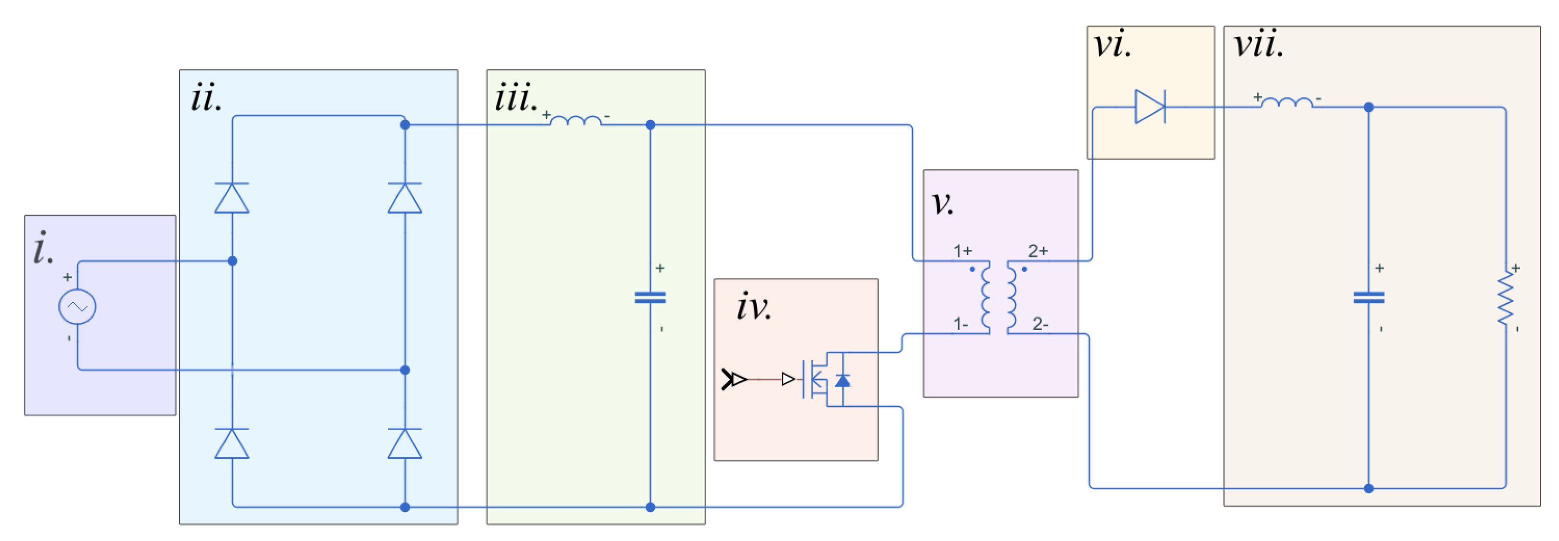
The SMPS, which is used to convert the AC supply voltage to a rated DC utilisation voltage, is very common in a large range of consumer appliances. The SMPS is the interface between the operational components of the device and the electricity supply network. Thus any disturbance on the network is directly coupled to the input of the SMPS. Whilst there are a vast number of designs of SMPS devices, many contain similar circuit topologies. Inspection of various, publicly available SMPS designs [13,14,15,16] indicates that the typical SMPS will likely include some iteration of the following:
- i.
- Input (from supply network)
- ii.
- Primary full bridge rectifier
- iii.
- LC filter
- iv.
- High-frequency switching
- v.
- Step-down transformer
- vi.
- Secondary winding rectification and
- vii.
- Secondary LC filter and output
The above provides a very basic outline of the typical SMPS and is presented graphically in Figure 1. Further circuitry is frequently used to limit the effects of switching transients, inrush current and short circuiting among other secondary functionalities [17].
The quantitative impact on the lifetime of a SMPS device due to sustained overvoltage is yet to be determined, however, typical failure modes for an SMPS have been investigated in [18]. The research indicates that of SMPS failures are due to electrolytic capacitor (EC) failures, due to MOSFET (high-frequency switching) failures and the remaining being related to failure of inductive elements and diodes. Based on this information, the EC has been identified as a critical point of failure within the SMPS and focus has been placed on the impact of sustained overvoltage on EC lifespan and failure rates in order to gain an understanding of the impact of sustained overvoltage on equipment lifespan.
3. Electrolytic Capacitors
ECs are used in a diverse range of products, including SMPS. SMPS designs will often utilise ECs in combination with an inductor at the output of the rectifier circuit to provide the DC bus for subsequent stages of the SMPS and this study has identified this to be the capacitor of most interest. The input LC filter capacitor is directly exposed to voltage variations due to the its location within the circuit.
While other power quality disturbances, such as high frequency ripple [19,20] and ambient temperature, will have an influence on capacitor lifetime, the focus of this paper is to investigate the relationship between the longevity of ECs and the magnitude of the supply voltage.
3.1. Representative Test Circuit
Capacitors can be represented using an equivalent circuit that accounts for the non-idealities of the component; Figure 2 [18] illustrates one such equivalent circuit.
For an electrolytic capacitor, this circuit accounts for , an equivalent parallel leakage resistance, , an equivalent series resistance (ESR), an equivalent series inductance (ESL), and , an equivalent series capacitance of the component. These parameters are present in all capacitors and the values of each parameter will vary between each. For the purposes of this study, the circuit shown in Figure 2 can be further simplified to include just the capacitance and ESR as the effects of and ESL have little impact on the results of the testing scenarios presented in this paper [21].
3.2. Failure Mode of Electrolytic Capacitors
Capacitors have different failure mechanisms dependent on the stress to which they have been exposed. Immediate, catastrophic failure can be the result of extreme overvoltage or electrolyte leakage. Another common capacitor failure mode is a gradual increase of ESR and a decrease of capacitance beyond allowable design tolerance levels [20]. The ESR of a capacitor can be calculated using (1) [22].
where:
- is the ideal capacitance of the component, directly correlated with the surface area of the capacitor plates, the dielectric constant and length of space between plates that is filled with electrolyte;
- f
- is the frequency of the current flowing through the capacitor;
All other variables are as referred to in Figure 2.
As discussed in [22], the resistive components of Figure 2 represent losses due to leakage current () and resistance of the physical components of the capacitor (). The total ESR of a capacitor is capable of increasing for a number of reasons, the most important cause for this study being due to the evaporation of electrolyte [23], which decreases the value of thereby increasing ESR as per (1), noting that both and are not affected by the evaporation of electrolyte. Electrolyte evaporation is capable of occurring when the capacitor operates at an increased temperature for an extended period of time [20,23]. An increased operating temperature of a capacitor can be due to ambient conditions or prolonged exposure to high voltage and is the result of increased ohmic losses within the component [24]. The authors of [25] state that a capacitor is considered to have failed when the ESR value of a capacitor has increased to 2.8 times the initial value (ESR0).
4. Test Device Design
For various reasons including cost, complexity and maintaining focus on the relationship between voltage levels and EC lifetime, it is neither feasible nor desirable to undertake assessment of actual SMPS devices. As such, in order to evaluate the impact of sustained overvoltage on the EC of interest, a test device (TD) was designed and fabricated to mimic the front-end (i.e., AC/DC conversion stage) of a typical SMPS.
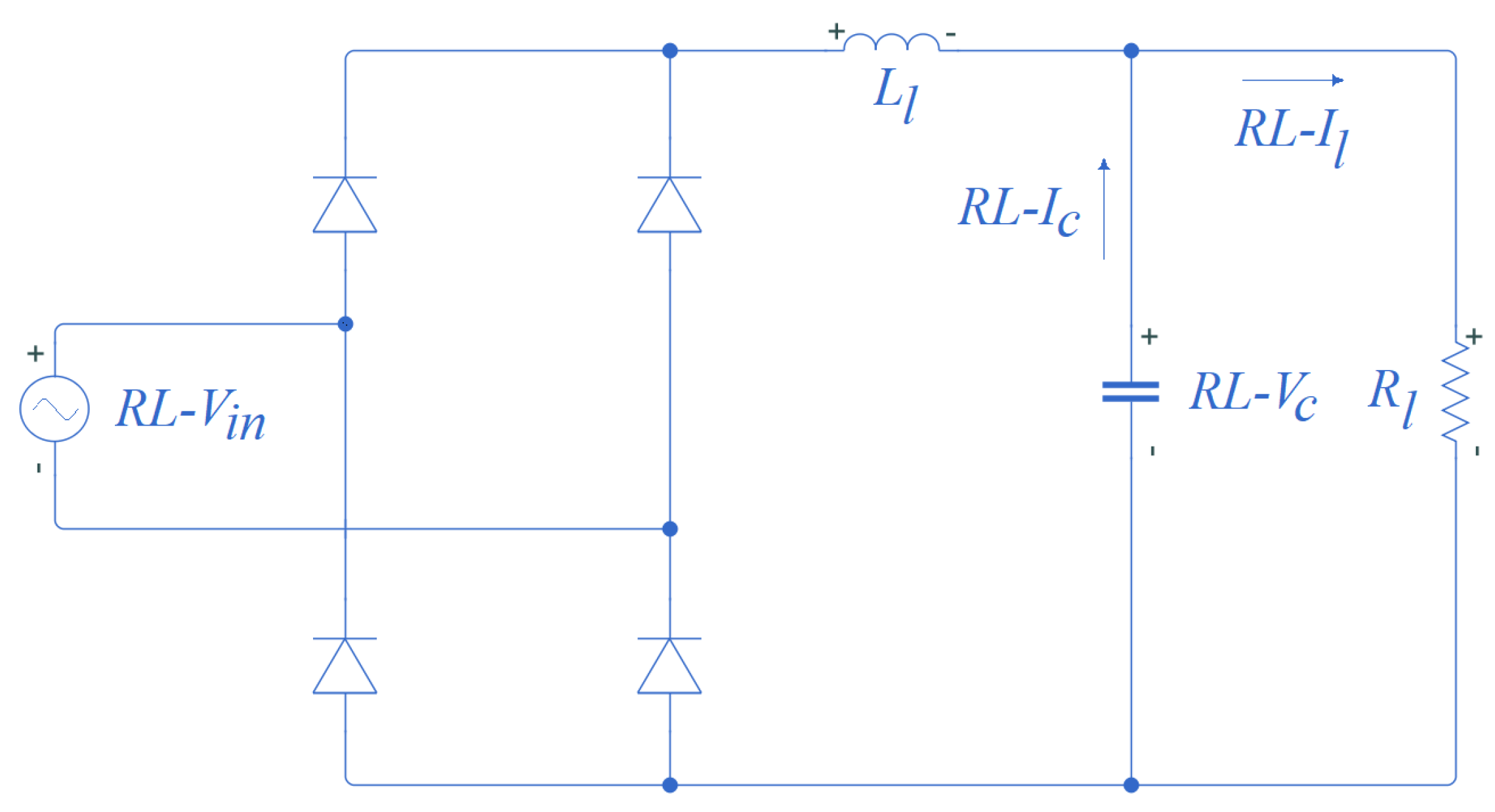
The TD was designed to focus on the relationship between the lifespan of the DC-link capacitor and input voltage magnitude whilst allowing for reduced cost and complexity. However, it was important that the TD accurately reproduce the performance of a typical SMPS front-end. In order to simplify and optimise the TD, all components beyond the bridge rectifier-LC filter combination were reduced to a representative load resistor. Computer simulations were undertaken to determine if this simplification provides an appropriate representation of a SMPS with regard to the front-end LC filter and overvoltage conditions. Another advantage of the use of a bespoke TD design is that it removes variabilities in the design and manufacturing practices of proprietary SMPS devices.
4.1. Computer Simulation
A computer simulation tool, Simulink, was used to evaluate whether simplifying the test circuit as described above was an acceptable approach to investigate the impacts of sustained overvoltage. The model shown in Figure 1 and the simplified model shown in Figure 3 were used to determine the impact of replacing components iv.–vii. with a simple load resistor.
In order to ascertain the feasibility of this simplification, the input voltage and current waveforms of the full model, as presented in Figure 1, were compared with the simplified model as per Figure 3, and an FFT comparison was undertaken.
Figure 4 shows the output voltage waveform of both simulation circuits, where:
Figure 4 indicates that the use of a resistive load does not significantly impact the voltage waveform across the DC-link capacitor, supplying the subsequent sections of the simple SMPS.
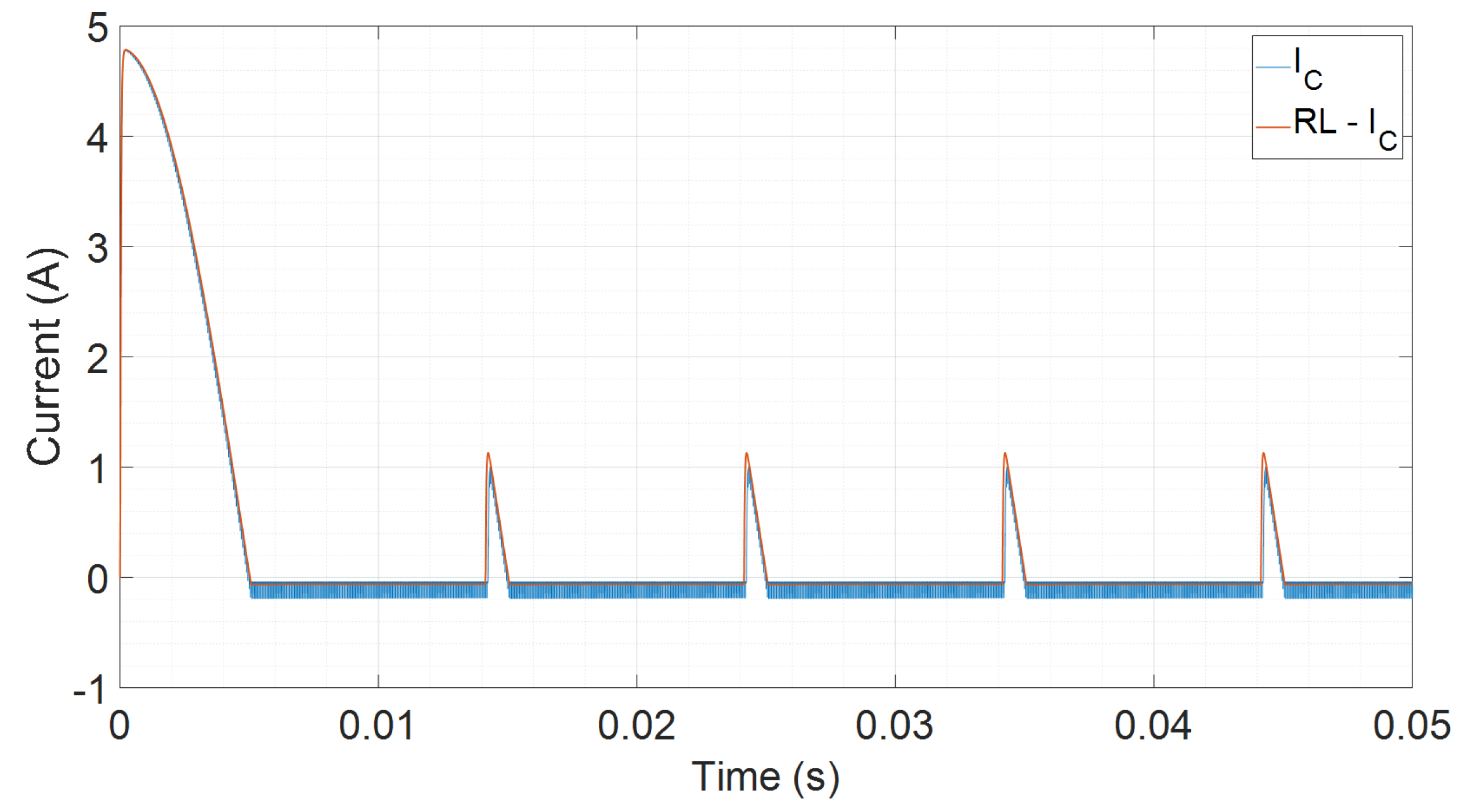
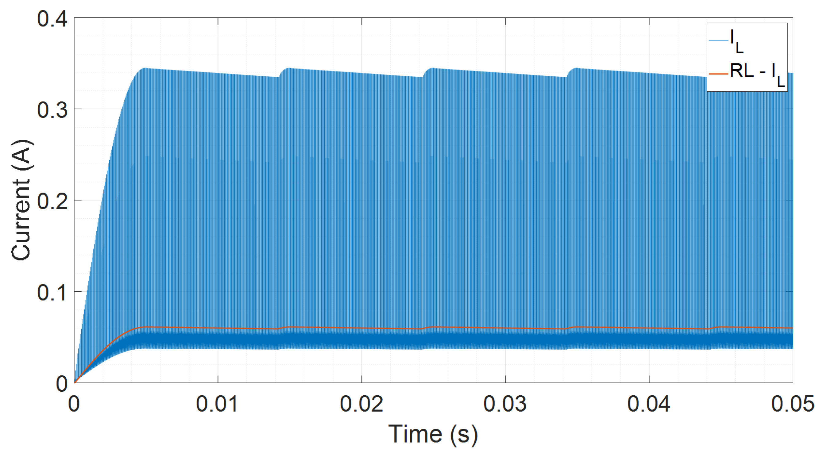
Figure 5 and Figure 6 provide comparison of the current through the DC-link capacitor and load respectively for both circuits.
- is the current through the DC-link filter capacitor to the simple SMPS load;
- is the current through the DC-link filter capacitor when the load is represented by a simple resistor;
- is the current supplied to the simple SMPS load;
- is the current supplied to the simple SMPS load when the load is represented by a simple resistor.
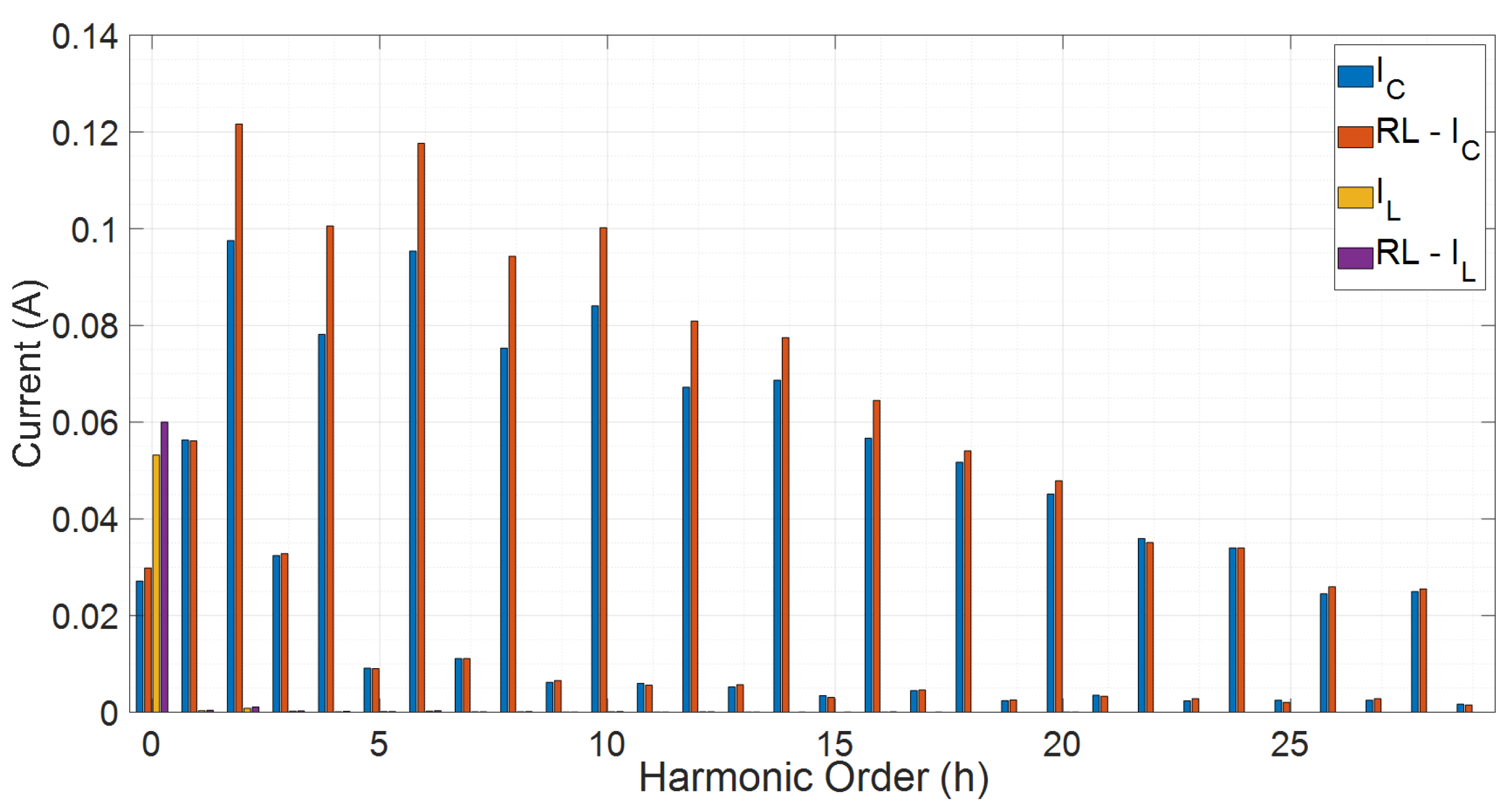
As can be seen, there is a significant difference between the current waveforms for the complete and reduced circuit topologies. This difference in current is due to the switching MOSFET that is present in the full SMPS circuit. The large current spikes seen in and in Figure 5 and Figure 6 respectively occur when the MOSFET switches states causing an inrush of current through the inductive component of the transformer. This switching occurs at high frequency to reduce the required size of the step-down transformer and reduce losses within the circuit [17]. In order to determine whether this high frequency switching renders the resistive load reduction inappropriate for the study, an investigation of the FFT of the resulting current of both models was undertaken, shown in Figure 7.
It can be seen that the resistive load circuit current has a very similar harmonic spectrum to that of its counterpart in the simple SMPS circuit. The (DC) current for both circuits is comparable, suggesting that the average current supplied and therefore power consumption for the simplified circuit is representative of the complete design. It should also be noted that high-frequency currents are detrimental to the lifetime of an EC [20]. As such, omission of these current spikes, as provided by the resistive load model, introduce further advantages to the study by focussing the rate of lifespan degradation due solely to sustained overvoltage conditions as opposed to a combination of power frequency and high frequency voltage components.
4.2. Design of Test Device
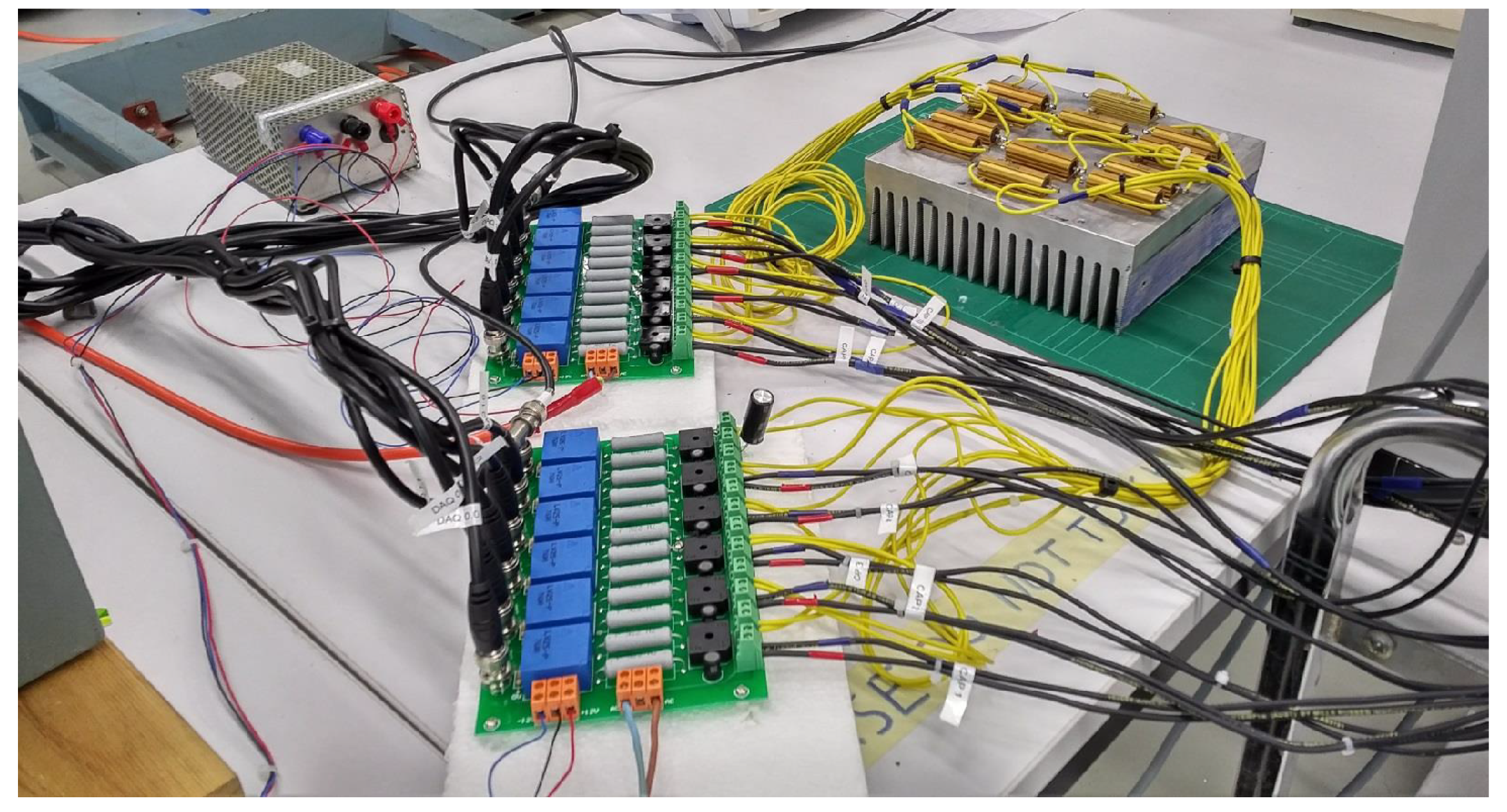
Based on the outcomes of the computer simulation, it can be confirmed that a reduction of the simple SMPS system to a rectifier-LC filter combination powering a resistive load is appropriate for the study. The TD was designed as per the schematic shown in Figure 3, with six TDs mounted on each test board, enabling connection to data acquisition equipment and the EC under test. The physical layout of the test board is shown in Figure 8. The parameters and ratings were chosen to resemble a common power supply front-end capable of powering a small to medium electronic device (e.g., LED driver, small monitor, generic AC/DC power converters). Using this circuit topology, the component under test is solely the EC. Selected ratings and component values for the TD are given in Table 1.
5. Design of Experiment and Methodology
The purpose of this study was to evaluate the impact of sustained overvoltage on electronics-based consumer equipment lifespan. The study focuses on SMPS as a very common electronic load. Accordingly, the impact of overvoltage on the lifespan of the EC within the SMPS, as a likely point of failure, has been established through the use of the simplified TD. In order to complete this investigation, it was necessary to obtain a large dataset of the time required for capacitors to fail when exposed to a range of input voltages. Failure was defined to have occurred when the ESR value reached 2.8 times the original value (which is equivalent to failure as discussed in Section 3.2).
The capacitor which was selected for the study has a minimum rated lifetime of 2000 h. Given this expected lifespan, it is time prohibitive to undertake lifetime testing of a large number of these capacitors under normal operating conditions. Consequently, a method was developed that involved lifespan evaluation at an increased temperature in order to accelerate the lifetime ageing of the capacitors to ensure that sufficient volume of time to failure data could be collected for evaluation.
5.1. Operating Temperature
As outlined in Section 3, a typical failure mode for ECs is an increase in ESR and commensurate decrease of capacitance to an unacceptable level. This increase in ESR is due to the evaporation of electrolyte within the casing which is influenced by the temperature at which the component operates. This is supported by [26] which states that the expected lifetime of a capacitor can be estimated using (2).
where:
- is the rated lifetime under maximum operating temperature;
- is the maximum rated operating temperature;
- T
- is the actual operating temperature.
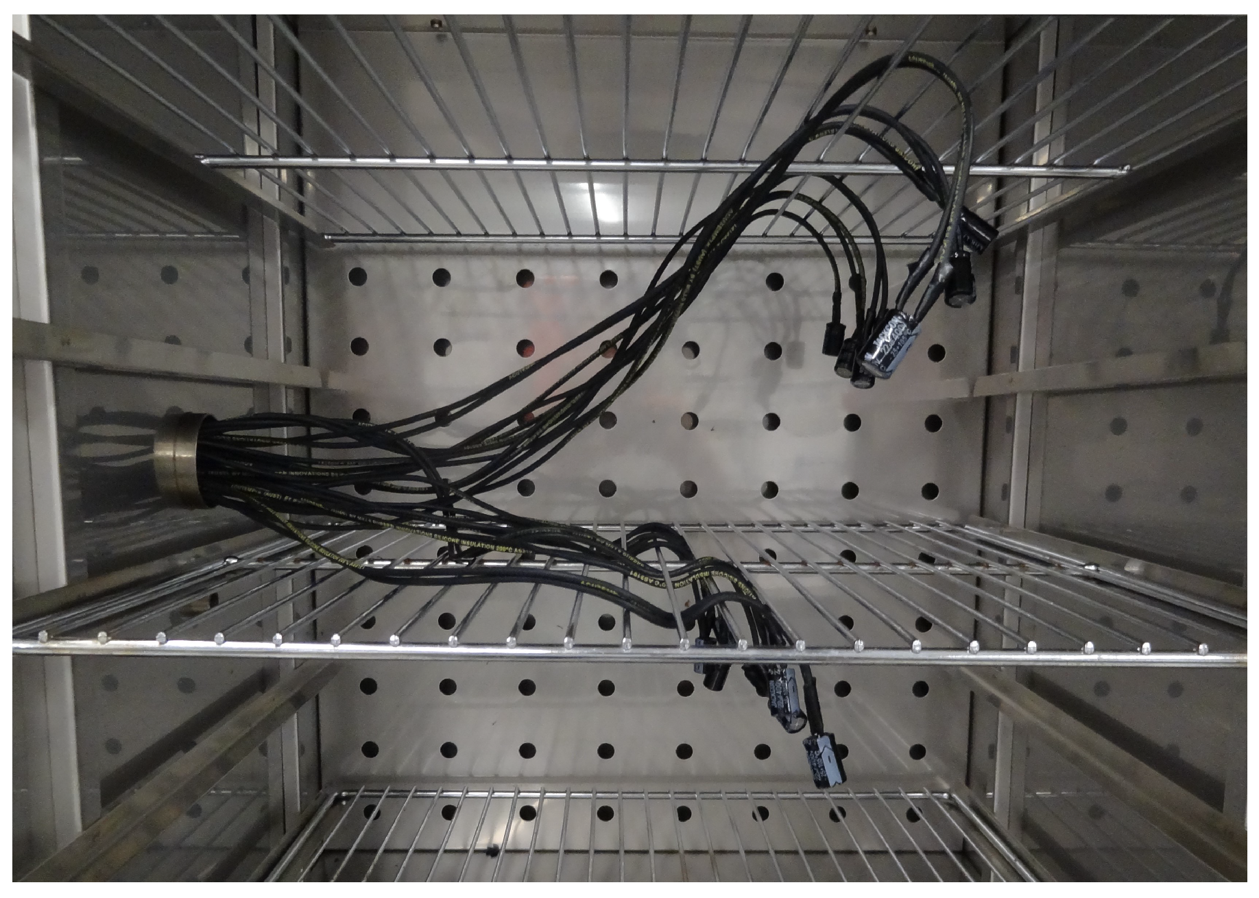
However, it is identified in [26] that (2) is only valid for the allowable working temperature range, typically −40 °C < T < 105 °C. Such considerations were taken into account when selecting the operating temperature range for the completion of testing, that is, the elevated operating temperature selected was determined through an iterative process to ensure spurious results were not introduced into the cause of failure. This resulted in a continuous operating temperature of 160 °C being selected for the duration of testing. This operating temperature allowed reduced testing time being required whilst allowing significant data to be collected without introducing additional failure modes. A high precision laboratory oven was used to provide a stable testing environment at 160 °C. Figure 9 show the ECs located in the laboratory oven with cables for connection back to TDs.
5.2. Measurement Process
Throughout the course of the experiment, the capacitance, ESR and capacitor ripple voltage were measured at regular intervals. In order to measure capacitance and ESR values, a high precision LCR meter was used (GW Instek LCR-819). Prior to testing, initial values were obtained and measurements were taken at 24-hour intervals to monitor the variation over the course of each test scenario. Each measurement was taken after the TD had been switched off and the capacitor had returned to room temperature. This was an important step as both ESR and capacitance are directly affected by the temperature of the component [26].
Both [18,25] conclude that the magnitude of the peak-to-peak voltage, (), measured across the DC-link capacitor is a reliable indicator of the ESR. was monitored throughout the course of the experiment, however, no consistent relationship between and ESR could be established. Off-line measurement of ESR was therefore used as it was determined to be a simpler, more reliable indicator of the degradation rate for each capacitor.
5.3. Test Voltages
The voltages applied to the TD were 230, 240, 250, 260 and at . This equates to a voltage range of 100–117% of nominal voltage (). With the magnitude of voltage being the only variable, it is reasonable to suggest that any discernible change in degradation will primarily be due to the magnitude of voltage applied. The experimental methodology at each voltage level was as follows:
- The capacitors were placed in the preheated oven and the power was switched on;
- The test was then left to run for 24 h, at which point the power was switched off and the capacitors were removed from the oven;
- Once returned to room temperature, the capacitance and ESR was measured for each capacitor and compared to their original values;
- The capacitors were then placed back into the oven and the experiment resumed;
- The above process was repeated until the ESR of the capacitors under test reached 2.8 times the original value.
The above process allowed for a clear degradation model to be determined for the capacitor under test using product lifecycle management (PLM) software. At the completion of the experiment, the PLM software was used to determine the relationship between input voltage and capacitor lifespan.
5.4. Analysis Software
PLM software is commonly used for determining reliability prediction, expected failure modes and refining the design of products. For this study, accelerated life testing (ALT) and degradation software modules were used to evaluate the rate of degradation and probability of failure of the ECs which was then used to determine the relationship between voltage magnitude and life of the EC [27]. In the interest of using as much data as practicable, the software package was used to estimate the time to failure (TTF) for ECs that did not completely fail by the completion of the testing scenario.
In total, 92 capacitors were tested across all voltage levels considered, including the additional tests at different temperatures during the iterative process discussed below. From this, a subtotal of 77 capacitors were tested across the defined range of voltages at 160 °C, and are shown in Table 2. The average time of testing for these capacitors was approximately 70 h and the total testing time was 612 h. As shown in Table 2, comparatively more capacitors were tested at and . These were also the voltage magnitudes used during the iterative process to determine appropriate temperature levels discussed in Section 5.1 to develop an understanding of expected time frames required. A reduced number of capacitors for the higher voltage levels was found to be sufficient to develop an acceptable relationship of voltage with lifetime degradation acceleration as discussed in the following section.
6. Results and Analysis
In the first instance, results of the laboratory evaluation are presented as probability density functions (PDFs) of the time to failure of the ECs with respect to input voltage. Using these PDFs, it is possible to derive an equation which relates the input voltage magnitude to the loss of life of the EC [28].
6.1. Time to Failure PDFs
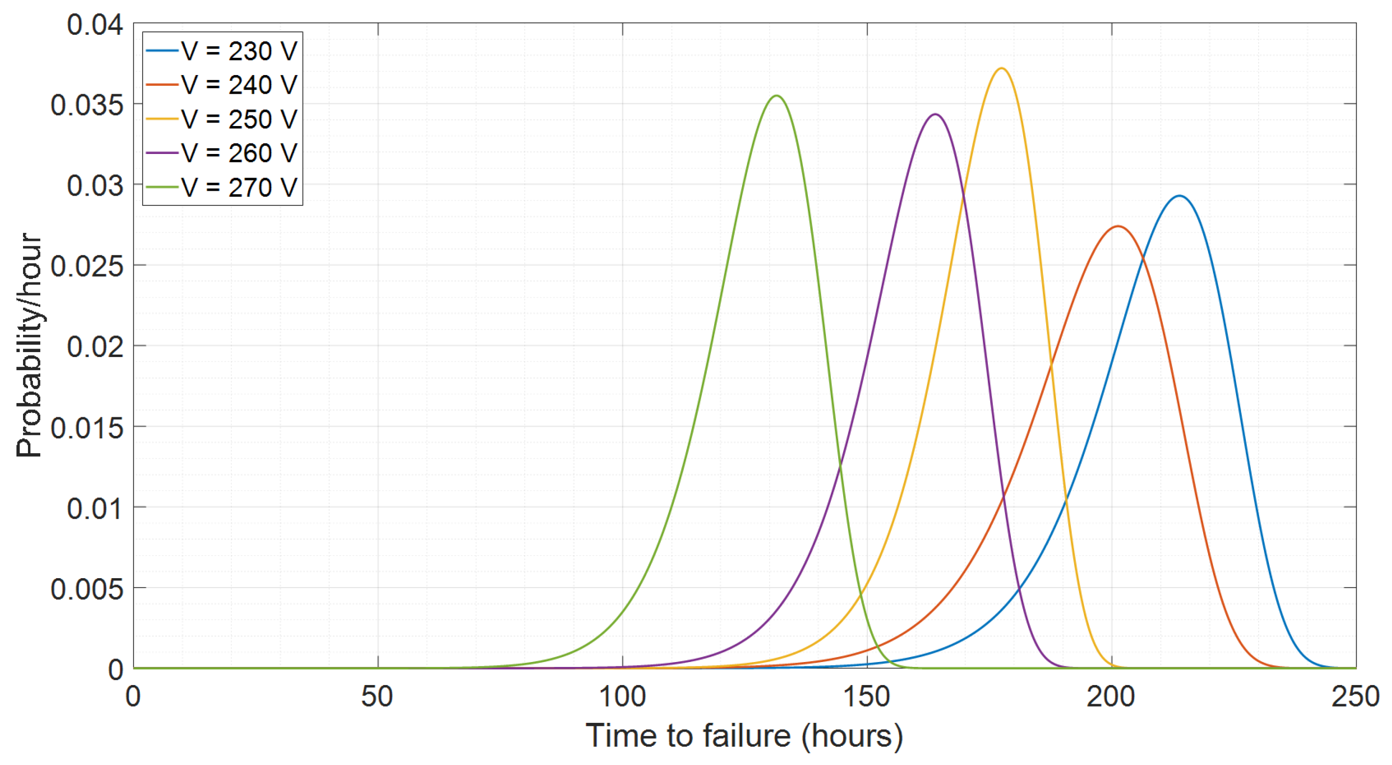
Figure 10 shows the PDF of time to failure for each of the voltage magnitudes evaluated. These PDFs were obtained by entering the TTF values (estimated calculation values used where required, as per Section 5.4) into the PLM software package and then calculating the PDF for each data set. As such, Figure 10 provides a graphical representation of the probability of failure based on the time in operation and operating voltage magnitude. The location on the x-axis of the peak of each curve defines the time (in hours) at which of the capacitors have failed for the given voltage level. Figure 10 illustrates that there is a clear decline in the average TTF as the voltage applied to the capacitor increases. For example, it can be seen that the median lifespan for an EC when supplied at is times larger than the average lifespan when supplied at . Figure 10 also shows that the shortest expected life time of a capacitor (i.e., <5%) operating at is approximately equal to the longest expected lifetime of the capacitor operating at .
6.2. Acceleration Factor for System Failure Prediction
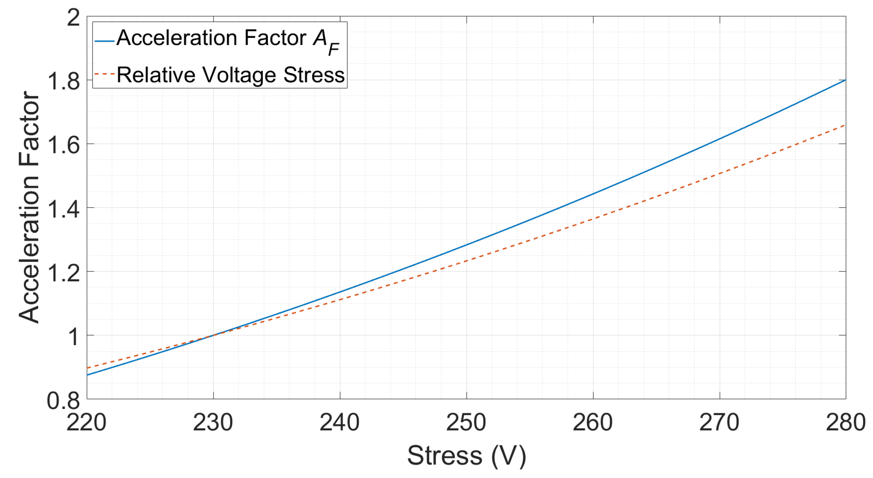
The data shown in Figure 10 can be used to derive an equation which relates the input voltage to the lifespan of the EC. Such an equation uses the data shown in Figure 11 which was obtained through degradation modelling using TTF values obtained through experimentation. It shows the impact that an increased voltage has on the expected lifetime of a SMPS system that is designed for a rated voltage of . In this case the system is the test device and the failure mode is the degradation of the front-end filter capacitor beyond acceptable values. The nominal system/equipment voltage of is used here in place of the specific capacitor rated voltage to align with the tests performed and for ease of interpretation of results. The resultant graph determines the Acceleration Factor () of the lifetime of the capacitor due to applied stress which in this study is the magnitude of applied voltage. can be calculated using (3).
where:
- is the rated lifetime of the component in hours;
- is the accelerated lifetime measured throughout the study.
To accurately quantify the impact that voltage has on the lifetime of a rated device, the inverse power law (IPL) stress model was applied. This is a common stress model used for ALT when the acceleration stress is non-thermal [30]. Whilst the capacitors were exposed to an elevated temperature, the stress factor of interest for this study was the operating voltage. The IPL uses (4) to determine the expected life of a component.
where:
- V
- is the stress level;
- K
- and n are model parameters to be determined.
Using ALT modelling of the collected data, the parameters K and n were determined to be:
- ;
- .
The acceleration factor for an IPL stress model can be calculated with (5).
where:
- is the voltage magnitude used in the ALT;
- is the rated voltage.
This shows that the life acceleration of a component is directly related to the ratio of the instantaneous stress and the rated stress. Placing the result of (5) into (3), (4) becomes (6).
Using (6), the lifetime of a known SMPS can be estimated based on the sustained voltage magnitude it is exposed to. Equation (6) is a representative equation in which each system is likely to have different values for n that must be determined experimentally and is reliant on the components used, design topologies, voltage range and operating temperature. This is an important result as it reduces the system to a very simple relationship involving only rated parameters and applied stress. For example, a device has been tested and has a rated lifetime of 2000 h with an operating voltage of . If the device is instead exposed to , the expected lifetime can then be calculated using (6).
For this device, the expected lifetime was reduced by due to the increased operating voltage, resulting in the device requiring repair or replacement, a direct cost to the customer.
Further, investigation of Figure 11 and (3) suggest that the lifetime acceleration factor can be reduced below 1 by limiting the operating voltage below design values. This is an important outcome as it suggests that lower voltages, whilst maintaining reliable operation of the SMPS, would be advantageous to the lifetime of the EC and therefore the device as a whole.
The resulting acceleration factor for the various test voltages can be compared to the voltage stress component of the more traditional EC failure models from [29] where (7) defines the EC base failure rate and the voltage stress component resides within the square brackets.
where:
- is the base failure rate (failures/ hours);
- S
- is the ratio of operating to capacitor rated voltage;
- T
- is the ambient temperature.
For an EC applied waveform as per of Figure 4 with d.c. ripple of approximately at each voltage level the resulting EC voltage stress component from (7) was determined and plotted (relative to value) within Figure 11. It is noted that the results show reasonable agreement between this study and the method from [29] with a slightly higher acceleration factor resulting from the work presented in this paper.
7. Summary and Future Work
In this study, laboratory evaluation of a specially designed test device has been undertaken in order to develop a preliminary understanding of the relationship between the lifespan of a key component of the ubiquitous SMPS and input voltage. Specifically, the study has assessed the relationship between input voltage magnitude and the lifespan of an EC that is used in the DC bus of many SMPS designs. The specially designed test circuit was used in order to reduce both the cost and complexity of the experimental work and to reduce the number of variables that were subject to assessment. Verification that the test device accurately reproduced the performance characteristics of an actual SMPS was undertaken using a computer simulation package.
An accelerated ageing test strategy was developed for the purposes of this study. This accelerated ageing test strategy reduced the amount of time required to collect a volume of data sufficient to determine the relationship between input voltage and lifespan of the EC.
The outcomes of this study clearly show a strong relationship between input voltage and EC lifespan with lifespan decreasing as input voltage increases. For example, it can be seen that the median lifespan for an EC when supplied at is times the median lifespan when supplied at . In fact, even the shortest estimated EC life when supplied at is longer than the maximum estimated life when supplied at .
The outcomes of this study are both important and relevant as they show a direct relationship between component loss of life and input voltage. Given the relatively high voltage levels observed in Australia (and likely other parts of the world) and the increasing penetration of dispersed rooftop solar PV generation which is leading to additional voltage rise and higher light load voltages [5,6], the relationship between input voltage and component lifespan is highly topical.
The outcomes of this experimental work clearly show an increased rate of capacitor degradation due to sustained overvoltage. Inspection of the PDF of each scenario (Figure 10) shows a clear decline in the expected average TTF across all scenarios where the only operational variable was the applied . This outcome makes it reasonable to suggest that an increase in operating voltage is likely to decrease the average TTF of an EC commonly used for standard SMPS devices. This was further investigated to obtain an acceleration factor in which the TTF was found to be a function of the operating and rated voltages. A derating curve can be determined for systems to better understand the effect of voltage levels on the lifetime of SMPS and whilst the graphics presented in this paper were derived for a single system design, it is expected that similar results are likely to be obtained for the majority of similarly designed power supplies. This can be suggested due to the uniformity of systems and the EC component itself.
Future Work
The work presented in this paper focuses on the effects of sustained overvoltage on a generalized SMPS design that connects to the network supply via a rectifier-LC filter combination. This is representative of many similarly designed hardwares; however, LC filters are very common across a wide range of devices, not just SMPS. It would be beneficial therefore to focus further study on the rate of degradation on ECs connected to a range of devices and for a wide range of EC types.
The voltages waveforms supplied to the test devices in this study were undistorted, sinusoidal waveforms of varying magnitudes. Given capacitors are susceptible to increased ripple currents and the presence of harmonics, and likely to lead to further lifespan reduction, an area for future work would be including specified levels of harmonic distortion to the applied voltage waveforms.
Continued testing and measurement could lead to developing a clearer understanding of derating curves and lifetime acceleration factors related to ECs and other capacitor types in a range of operating scenarios and device types. For example, PV inverter systems commonly use capacitors as a front end connection in an attempt to filter high frequency distortion [31]. Due to the continued rise in popularity of photovoltaic systems and their noted impact on voltage levels, it is suggested that a thorough investigation into the effect that sustained overvoltage has on common front-end filters for inverters should be undertaken.
8. Conclusions
A detailed inspection of commonly connected equipment reveals the prevalence of SMPS devices and determines that a common weak link for these devices is the DC-link capacitor. A TD was designed that placed the focus directly on this capacitor and exposed it to a range of voltage levels. The results clearly revealed the link between operating voltage and the lifetime of ECs. This causal link has been presented mathematically and the relationship suggests that the ratio between the applied voltage and designed nominal voltage has a large impact on the lifetime of the capacitor. For the case study capacitor the equipment lifetime was shown to display an inverse cubic relationship with voltage stress, for example, when exposed to a sustained increase in operating voltage to 250 V (20 V above nominal) the equipment lifetime reduced by 22%.
Author Contributions
Conceptualization, J.D. and P.C.; methodology, J.D., P.C. and S.E.; software, J.D.; validation, P.C., S.E. and D.R.; formal analysis, J.D. and S.E.; original draft preparation, J.D. and S.E.; review and editing, D.R. All authors have read and agreed to the published version of the manuscript.
Funding
The research reported in this paper was completed as part of a project titled ‘The Impact of Sustained Overvoltage Levels on Network and Customer Equipment’, funded by the Australian Strategic Technology Program (ASTP).
Institutional Review Board Statement
Not applicable.
Informed Consent Statement
Not applicable.
Data Availability Statement
Not applicable.
Conflicts of Interest
The authors declare no conflict of interest. The funders had no role in the design of the study; in the collection, analyses, or interpretation of data.
Abbreviations
The following abbreviations are used in this manuscript:
| AC | Alternating Current |
| ALT | Accelerated Life Testing |
| AS | Australian Standard |
| DC | Direct Current |
| EC | Electrolytic Capacitor |
| ESL | Equivalent Series Inductance |
| ESR | Equivalent Series Resistance |
| FFT | Fast Fourier Transform |
| IPL | Inverse Power Law |
| LC | Inductor-Capacitor |
| LCR | Inductance-Capacitance-Resistance |
| LED | Light-Emitting Diode |
| LV | Low Voltage |
| MOSFET | Metal–Oxide–Semiconductor Field-Effect Transistor |
| Probability Density Function | |
| PLM | Product Lifecycle Management |
| PQ | Power Quality |
| PV | Photovoltaic |
| RMS | Root-Mean-Square |
| SMPS | Multidisciplinary Digital Publishing Institute |
| TD | Test Device |
| TTF | Time To Failure |
References
- Halliday, C.; Urquhart, D. Voltage and Equipment Standards Misalignment; The Electric Energy Society of Australia: Canberra, Australia, 2011. [Google Scholar]
- AS 60038-2012; Standard Voltages. Standards Australia: Sydney, Australia, 2012.
- AS 61000.3.100-2011; Electromagnetic Compatibility (EMC), Part 3.100: Limits—Steady State Voltage Limits in Public Electricity Systems. Standards Australia: Sydney, Australia, 2011.
- Australian PV Institute. Australian PV Market since April 2001. Available online: https://pv-map.apvi.org.au/analyses (accessed on 17 December 2021).
- Karimi, M.; Mokhlis, H.; Naidu, K.; Uddin, S.; Bakar, A. Photovoltaic penetration issues and impacts in distribution network—A review. Renew. Sustain. Energy Rev. 2016, 53, 594–605. [Google Scholar] [CrossRef]
- Thomson, M.; Infield, D. Impact of widespread photovoltaics generation on distribution systems. IET Renew. Power Gener. 2007, 1, 33–40. [Google Scholar] [CrossRef]
- AS 4777.2-2020; Grid Connection of Energy Systems via Inverters, Part 2: Inverter Requirements. Standards Australia: Sydney, Australia, 2020.
- Elphick, S.; Smith, V.; Gosbell, V.; Barr, R. Characteristics of Power Quality Disturbance Levels in Australia. In Proceedings of the 2012 IEEE 15th International Conference on Harmonics and Quality of Power (ICHQP), Hong Kong, China, 17–20 June 2012; p. 61. [Google Scholar]
- Seljeseth, H.; Sand, K.; Fossen, K. Laboratory Tests of Electrical Appliances Immunity to Voltage Swells. In Proceedings of the InCIRED 2009—20th International Conference and Exhibition on Electricity Distribution-Part 1 2009, Prague, Czech Republic, 8–11 June 2009. [Google Scholar]
- Seljeseth, H.; Rump, T.; Haugen, K. Overvoltage Immunity of Electrical Appliances Laboratory Test Results from 60 Appliances. In Proceedings of the 21st International Conference on Electric Power Distribution (CIRED), Frankfurt, Germany, 6–9 June 2011. [Google Scholar]
- Cobben, J. Power Quality: About the Problems and Solutions; CO-Education: Arnhem, The Netherlands, 2012. [Google Scholar]
- James, R.; Su, Q. Condition Assessment of High Voltage Insulation in Power System Equipment; The Institution of Engineering and Technology: London, UK, 2008. [Google Scholar]
- Power Integrations. LinkSwitch-XT Low Cost 2 W CV Power Adapter. p. 2. November 2005. Available online: http://www.farnell.com/datasheets/10037.pdf (accessed on 15 June 2017).
- Power Integrations. 12 W Universal Input CV Adapter, Design Idea. p. 2. February 2008. Available online: https://ac-dc.power.com/sites/default/files/PDFFiles/di91.pdf (accessed on 15 June 2017).
- Power Integrations. 3.8 W 2-Output Supply Using LNK623PG Design Example Report. p. 30. May 2009. Available online: https://ac-dc.power.com/sites/default/files/PDFFiles/der213.pdf (accessed on 15 June 2017).
- Texas Instruments. 230Vac Triac Dimmable 10W LED Driver Reference Design. p. 13. June 2013. Available online: http://www.ti.com/lit/df/slurac0/slurac0.pdf (accessed on 15 June 2017).
- Billings, K.; Morey, T. Switchmode Power Supply Handbook, 3rd ed.; McGraw-Hill Professional: San Francisco, CA, USA, 2011. [Google Scholar]
- Zheng-Yu, S.; Yu-Dong, L.; Tao, N.; Meng-Qi, L.; Jing-Dong, F.; Zhen-Wei, Z. The Real-time Fault Diagnosis of Electrolytic Filter Capacitors in Switching Mode Power Supply. In Proceedings of the 20th IEEE International Symposium on the Physical and Failure Analysis of Integrated Circuits (IPFA), Suzhou, China, 15–19 July 2013. [Google Scholar]
- Wohlfahrt, T.; Waniek, C.; Myrzik, J.; Meyer, J.; Schegner, P. Supraharmonic disturbances: Lifetime reduction of electronic mass-market equipment by the aging of electrolytic capacitors. In Proceedings of the 18th International Conference on Harmonics and Quality of Power (ICHQP), Ljubljana, Slovenia, 13–16 May 2018. [Google Scholar]
- Darmawardana, D.; Perera, S.; Robinson, D.; David, J.; Meyer, J.; Jayatunga, U. Impact of High Frequency Emissions (2–150 kHz) on Lifetime Degradation of Electrolytic Capacitors in Grid Connected Equipment. In Proceedings of the 2019 IEEE Power & Energy Society General Meeting (PESGM), Atlanta, GA, USA, 4–8 August 2019. [Google Scholar]
- Parler, S., Jr. Improved spice models of aluminum electrolytic capacitors for inverter applications. In Proceedings of the 2002 IEEE Industry Applications Conference, 37th IAS Annual Meeting, Pittsburgh, PA, USA, 13–18 October 2002. [Google Scholar]
- Deng, F.; Heng, Q.; Liu, C.; Cai, X.; Zhu, R.; Chen, Z.; Chen, W. Capacitor ESR and C Monitoring in Modular Multilevel Converters. IEEE Trans. Power Electron. 2020, 35, 4063–4075. [Google Scholar] [CrossRef]
- Chen, P.; Liu, J.; Zhang, H.; Chu, B. Increase of Capacitance of Thick Dielectrics by Fringe Effect. IEEE Trans. Dielectr. Electr. Insul. 2019, 26, 1716–1719. [Google Scholar] [CrossRef]
- Taufik, T. A flyback inverter without input electrolytic capacitor. In Proceedings of the 2017 International Electronics Symposium on Engineering Technology and Applications (IES-ETA), Surabaya, Indonesia, 26–27 September 2017; pp. 157–160. [Google Scholar]
- Chen, Y.-M.; Wu, H.-C.; Chou, M.-W.; Lee, K.-Y. Online Failure Prediction of the Electrolytic Capacitor for LC Filter of Switching-Mode Power Converters. IEEE Trans. Ind. Electron. 2008, 55, 6. [Google Scholar] [CrossRef]
- Kemet Electronics Corporation. Radial Aluminium Electrolytic Capacitors—ESH Series, 105 °C. Product Specification Sheet. 2013. Available online: https://www.farnell.com/datasheets/1794402.pdf (accessed on 15 June 2017).
- PTC. Windchill Product Lifecycle Management Software. Available online: https://www.ptc.com/en/products/windchill (accessed on 7 December 2020).
- Naiken, V.; Rathore, A. Accelerated temperature and voltage life tests on aluminium electrolytic capacitors: A DOE approach. Int. J. Qual. Reliab. Manag. 2015, 33, 120–139. [Google Scholar] [CrossRef]
- US Department of Defence. Reliability Prediction of Electronic Equipment, Military Handbook; MIL-HDBK-217F; US Department of Defense: Washington, DC, USA, 1995. [Google Scholar]
- Méndez-González, L.; Rodríguez-Picón, L.; Valles-Rosales, D.; Iniesta, A.; Carreón, A. Reliability analysis using exponentiated Weibull distribution and inverse power law. Qual. Reliab. Eng. Int. 2019, 35, 1219–1230. [Google Scholar] [CrossRef]
- Büyük, M.; Tan, A.; Tümay, M.; Bayındır, K. Topologies, generalized designs, passive and active damping methods of switching ripple filters for voltage source inverter: A comprehensive review. Renew. Sustain. Energy Rev. 2016, 62, 46–69. [Google Scholar] [CrossRef]
Figure 1.
Typical SMPS circuitry—shaded areas represent sections as defined by i.–vii. above.

Figure 2.
Equivalent circuit of a capacitor.

Figure 3.
Simulation circuit with load resistor simplification.

Figure 4.
Voltage Waveform Comparison.

Figure 5.
Current Waveform Comparison—Capacitor.

Figure 6.
Current Waveform Comparison—Load.

Figure 7.
FFT Comparison of the Full and Representative Models.

Figure 8.
Test board showing mounting of test devices and external resistive loads (capacitors are connected externally to enabled them to be located in laboratory oven).
Figure 8.
Test board showing mounting of test devices and external resistive loads (capacitors are connected externally to enabled them to be located in laboratory oven).

Figure 9.
ECs under test located in laboratory oven with cables for connection back to TDs.

Figure 10.
Probability Density Function (PDF) Plot.

Figure 11.
Acceleration Factor () due to Voltage (this study) and Relative Voltage Stress from [29].
Figure 11.
Acceleration Factor () due to Voltage (this study) and Relative Voltage Stress from [29].


Table 1.
Test Device Component Values.
| Characteristic | Value |
|---|---|
| SMPS Rated Power | 20 W |
| EC Capacitance | 47 μF |
| EC Rated Voltage | |
| EC Operating Temperature | −25 °C to 105 °C |
| EC Technology | Radial aluminium |
| Electrolyte | Non-solid |
Table 2.
Testing Time.
| Voltage Level | Number of Capacitors Tested | Average Length of Test (Hours) |
|---|---|---|
| 35 | 72.5 | |
| 15 | 55 | |
| 9 | 92 | |
| 9 | 70 | |
| 9 | 50 |
Publisher’s Note: MDPI stays neutral with regard to jurisdictional claims in published maps and institutional affiliations. |
© 2022 by the authors. Licensee MDPI, Basel, Switzerland. This article is an open access article distributed under the terms and conditions of the Creative Commons Attribution (CC BY) license (https://creativecommons.org/licenses/by/4.0/).
Share and Cite
MDPI and ACS Style
David, J.; Ciufo, P.; Elphick, S.; Robinson, D. Preliminary Evaluation of the Impact of Sustained Overvoltage on Low Voltage Electronics-Based Equipment. Energies 2022, 15, 1536. https://doi.org/10.3390/en15041536
AMA Style
David J, Ciufo P, Elphick S, Robinson D. Preliminary Evaluation of the Impact of Sustained Overvoltage on Low Voltage Electronics-Based Equipment. Energies. 2022; 15(4):1536. https://doi.org/10.3390/en15041536
Chicago/Turabian StyleDavid, Jason, Philip Ciufo, Sean Elphick, and Duane Robinson. 2022. "Preliminary Evaluation of the Impact of Sustained Overvoltage on Low Voltage Electronics-Based Equipment" Energies 15, no. 4: 1536. https://doi.org/10.3390/en15041536
Note that from the first issue of 2016, this journal uses article numbers instead of page numbers. See further details here.