
High-Frequency Non-Invasive Magnetic Field-Based Condition Monitoring of SiC Power MOSFET Modules


1
School of Electronics Engineering and Computer Science, Queen Mary University of London, London E1 4NS, UK
2
Department of Electronic and Electrical Engineering, The University of Sheffield, Sheffield S10 2TN, UK
*
Author to whom correspondence should be addressed.
Energies 2021, 14(20), 6720; https://doi.org/10.3390/en14206720
Submission received: 16 August 2021
/
Revised: 24 September 2021
/
Accepted: 5 October 2021
/
Published: 15 October 2021
(This article belongs to the Special Issue Reliability of WBG-Based Power Electronic Circuits in Electric Vehicles)
Abstract
:Current distribution anomaly can be used to indicate the onset of package-related failures modes in Silicon Carbide power MOSFET modules. In this paper, we propose to obtain the wire bond’s magnetic field profile using an array of Tunnel Magneto-Resistance (TMR) sensors, and characterise the small changes in the current density distribution to find the onset of the wire bond degradation processes, including wire bond lift-off, wire bond cracking, and wire bond fracture. We propose a novel condition monitoring technique where a non-galvanic high-bandwidth sensing and a reliability model monitor the health of the power switches. We designed a dedicated calibration set-up to examine the sensor array and calibrated to demonstrate the adequate sensitivity to a minimum 5% current anomaly detection in a single wire bond of the switching devices operating with 50 kHz switching frequency. We use a hardware-in-the-loop (HIL) experimental set-up to replicate wire bond-related failures in a 1200 V/55 A SiC MOSFET power module of a DC/DC Boost converter. Signal conditioning circuits are further designed to amplify and buffer the sensor readings. Experimental results showed the proposed technique is able to detect a wide range of package-related failures.

1. Introduction
Wide Bandgap (WBG)-based power module, as an emerging semiconductor technology, can address most of the performance requirements in the high frequency high density power electronic applications [1,2,3]. Higher temperature operation, higher voltage and current ratings, and lower conduction power loss make Silicon Carbide (SiC) and Gallium Nitride (GaN)-based devices strong candidates for high density power electronic applications [4,5]. However, failure characterization and lifetime assessment are still challenging problems in SiC devices [2,6]. Considering the differences of failure mechanisms in the conventional Silicon-based power modules, novel reliability monitoring technique is demanded to characterise all sorts of failure mechanisms in WBG devices [2,7,8,9]. Condition Monitoring (CM) is a passive technique for assessing the switch degradation level and the health of the power module [2,10,11]. CM techniques based on physics of failure (PoF) and electrical operational parameters are studied in the literature [2,12,13,14]. For wire bond (WB)-related failure modes, ON-state Drain–Source voltage [15] and body diode forward voltage [2] were used as the health indicators. Moreover, Junction-case thermal impedance is used as solder-related fatigue indicator [15]. Gate leakage current [16] is used to detect body diode failure.
When it comes to CM of WBG power modules in the high switching frequency levels (e.g., over 20 kHz), the said precursors, however, face some fundamental limitations:
(1) Measurement of the electrical-based fatigue precursors is sensitive to temperature and also requires special implementation techniques [2,3]. This limitation becomes more apparent in high frequency circuit designs considering the nominal higher switching frequency in WBG devices. This is mainly due to the fact that the measurement system based on the electrical parameters with galvanic connections are prone to EMI and high-frequency switching transients [13,14,17].
(2) In the high switching frequency operation (20 kHz and above), the overall switching losses are not just related to the health of e.g., a SiC power MOSFET itself, and can be related to the degradation of the driver circuit, environmental conditions, load, etc. [17]. Therefore, in monitoring the degradation over a long period, estimation of the device degradation using a measurement tool prone to degradation itself is unsatisfactory. The sensible approach is to develop an isolated CM system which cannot be affected by long term temperature cycling in mission profiles.
(3) The overall operational parameters in the SiC MOSFETs are considerably lower in value in comparison to those of the Si-based MOSFETs and IGBTs [11]. For example, considering 20% change in as the end of useful life criterion [2,17,18], the CM system of a SiC power module must be able to detect a 6 m to 10 m change in , which is costly and complicated to be measured accurately in 20 kHz frequency levels and above [17].
Thermo-mechanical cycling, caused by Coefficient of Thermal Expansion (CTE) mismatch during commonly higher temperature operation, is cited as the main factor in switch package-level degradation [2,9]. The main outcome of the switch degradation is mostly in the form of WB-related (WB heel cracking, WB lift-off, and WB fracture) or solder-related (solder cracking, solder delamination, and solder joint fatigue) failure modes [2]. WB-related failures are more common in SiC-based power modules in comparison to Si-based modules [2]. The main reason is the severe CTE mismatch between the SiC chip and the WB connection in the die area [19]. CTE value for Si, SiC, and Aluminum is 5 (C), 2.77 (C), and 24 (C) respectively, which shows a larger mismatch between the SiC-Al interface in comparison to the SiC-Al interface during thermo-mechanical cycling. This leads to having more probability in forming cracks and voids in the wire bond connection, and consequently, the wire bond lift off, crack, or fracture are more probable in the SiC-Al interface. In this regard, detection of the onset of WB fatigue can cover a wide range of failures in the power modules, specifically WBG-based power modules.
In the high-current power electronic circuits, accurate and high bandwidth current sensing is a major challenge. One common way of sensing current value in circuits with lower than 20 kHz frequency is resistive sensing using a high-precision low value resistor with very low parasitic elements [20]. In the case of isolated sensing, the use of Hall effect sensors is the most common. The low bandwidth and long delay time make the open-loop Hall sensor not suitable for applications with high frequency operation [4,21]. New generation of magnetic sensors based on Magneto-Resistance (MR) technology, including Anisotropic Magneto-Resistive (AMR), Giant Magneto-Resistive (GMR), and Tunnel Magneto-Resistive (TMR) sensors, with smaller size and increased sensitivity, are better candidates for high frequency current measurements [22,23]. Lower resistance change ratio (e.g., low signal-to-noise ratio) and limited bandwidth are the two limitations of AMR and GMR sensors respectively. These limitations have been overcome in the TMR sensors, as the state-of-the-art in MR sensors [21,23]. In addition, TMR has the lowest temperature drift, which is important for CM measurement.
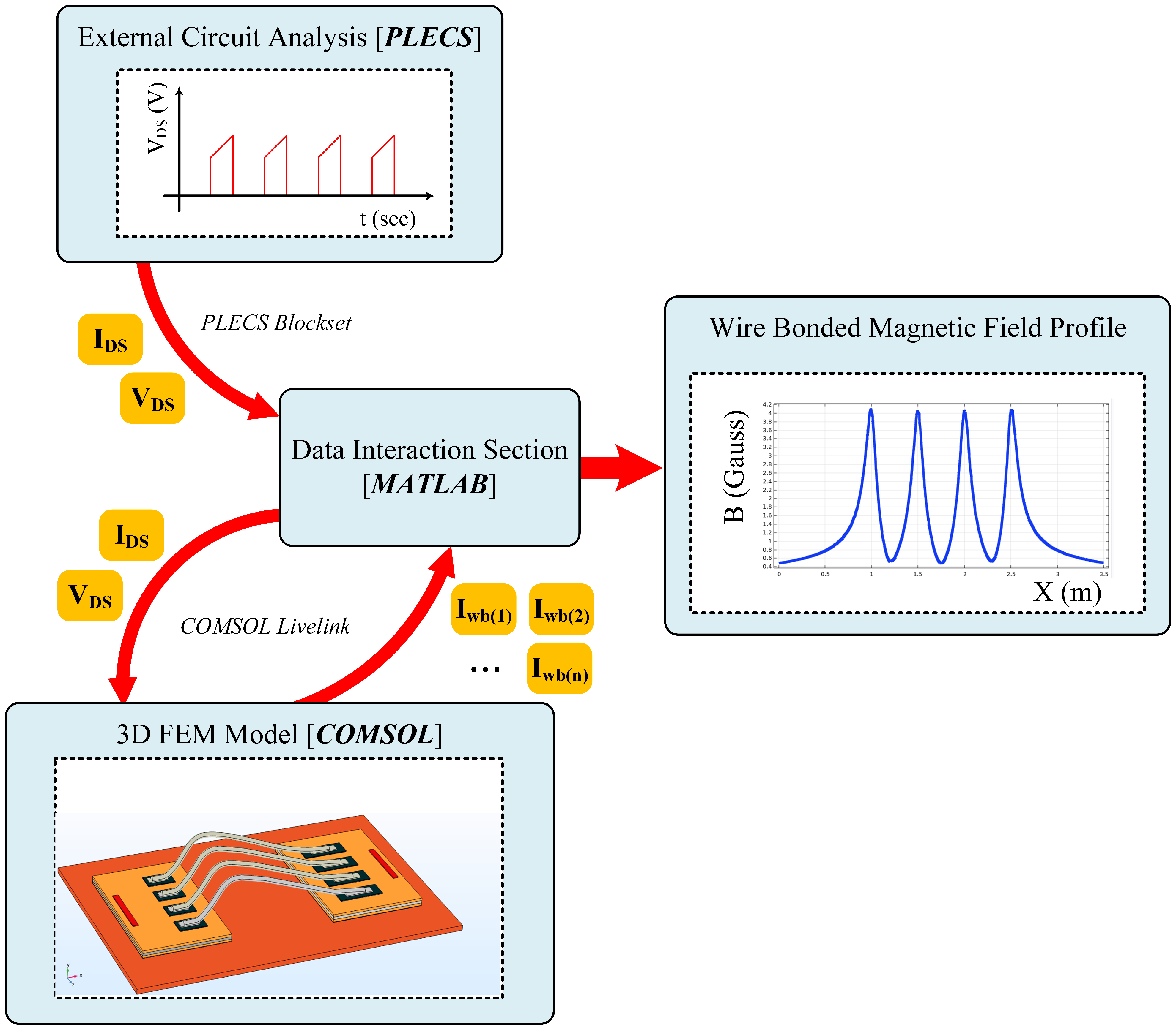
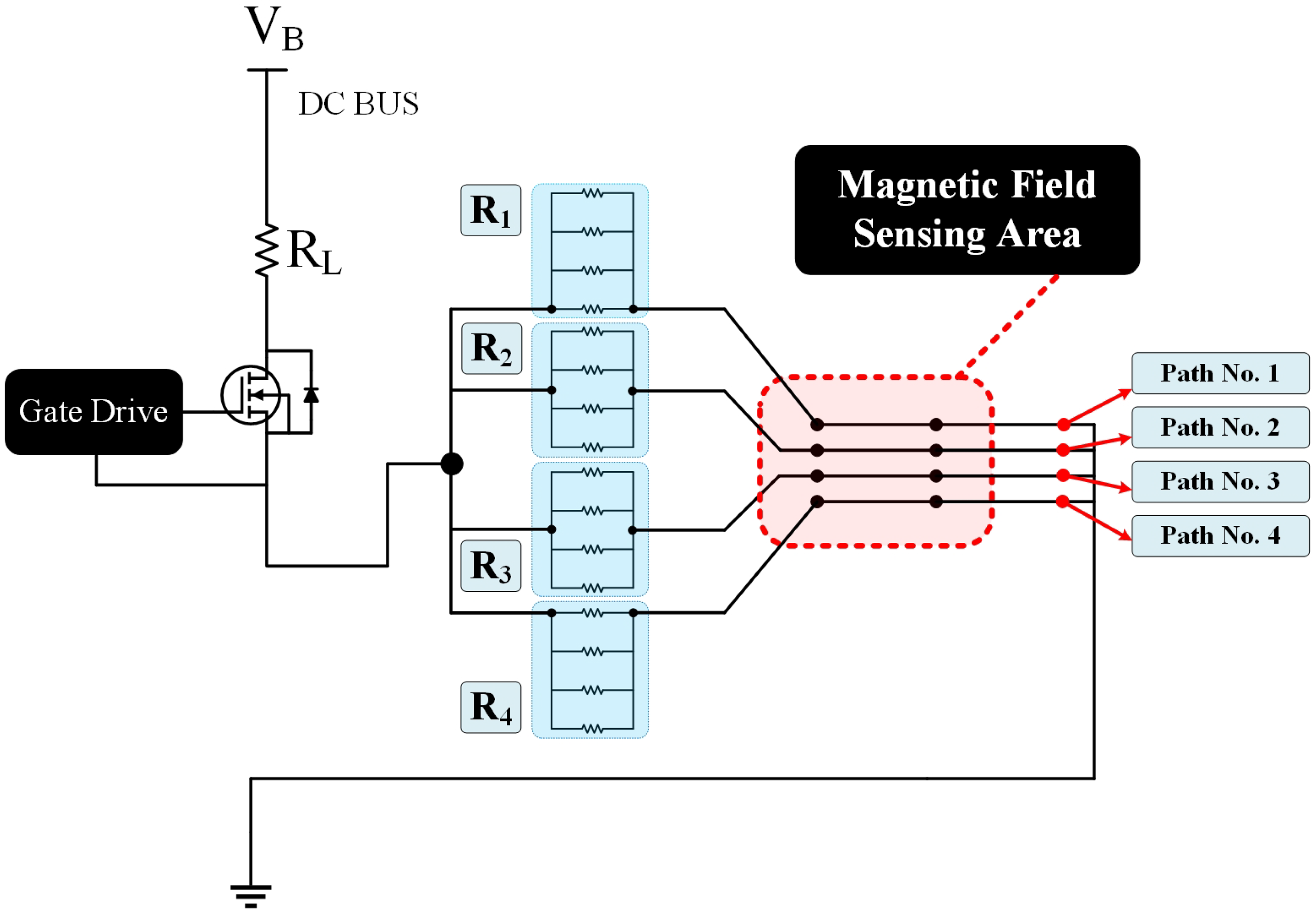
>In this paper, with the concentration on package-related degradation modes, an online CM technique for detecting failure onset of the SiC MOSFET power modules is proposed. In the package-related failure modes of SiC MOSFET, the degraded material, e.g., solder layer or WB connection to the die area has major change in electrical characteristics. The core idea of the proposed CM technique is to detect this change. Current conduction capability of a WB indicates its electrical characteristics. Non-transient changes or anomalies in the WB’s magnetic field pattern are perceived as the onset of device failure. An uneven current distribution leads to the generation of higher power loss in the non-degraded areas of the power module [2], leading to higher junction temperature and thermal stress on the solder layers. TMR sensor array will detect current distribution anomaly based on the WB’s magnetic field profile. To examine and calibrate the sensor array, a complete calibration process is proposed in this paper to achieve the most accurate readings, transferred to a real-time simulator (dSPACE SCALEXIO). In Figure 1, the main subsystems of the proposed CM technique are shown, where the signal acquisition is designed for high frequency operations. By sensing the Magnetic field, we will have a non-galvanic measurement and a robust CM technique against conduction noise and EMI issues, especially in high frequency operations. Moreover, using the isolated configuration, the CM system is not exposed to temperature and power cycling effects, and stability in long term can be achieved.
The rest of this paper is organised as follows. In Section 2, the magnetic field distribution inside the power module is formulated to provide an insight for the sensor design and placement. In Section 3, a calibration set-up will be designed and established for TMR sensor’s accurate readings, and detecting minimum 5% change in the magnetic field profile. Finally, in Section 4, using a 1200 V/55 A SiC MOSFET power module in a DC/DC Boost converter topology ( V, V, W), the CM technique is examined in a hardware-in-the-loop experimental set-up against the practiced WB-related failures in the power module.
2. Magnetic Field Basics in Power Module
Magnetic field formulation for the wire bonded connection of the power module is developed in Section 2.1. Furthermore, a coupled simulation platform for obtaining the real-time magnetic field of the power module is developed in Section 2.2. We use this simulation platform to validate the proposed failure detection in Section 4.
2.1. WB Magnetic Field Formulation
Maxwell’s equation suggests that for a specific amount of electrical current (I), which is passing from a single conductor with length of l, the surrounding magnetic flux density (B) is obtained as (1).
Based on the geometry of the conductor, the magnetic field of the surrounding area of the conductor can be characterized [24]. Depending on the WB terminal type, e.g., WB connection of two adjacent chips, chip to baseplate, and baseplate to terminal, the geometry of the WB is altered. Despite minor differences in the structure of WBs, the overall WB geometry is identical in all the connection types and can be modeled as a half hyperbola with one or two straight lines in the terminal areas (see Figure 2). The highest magnetic field is sensed at the center of the hyperbola-shaped wire, indicated by O in Figure 2. The total WB’s magnetic flux density in 2D dimensions can be obtained by Biot–Savart law [25,26] as (2).
where is the electrical current value passing through the WB, r is the distance between each differential element (point P) on the WB and the origin point (point O), and is the angle between the vertical axis and the vector of the differential element. In Figure 2, a single WB is considered, and the overall geometry as well as the explained vectors are shown. Based on the overall formula of a hyperbola structure, r can be written based on as (3).
where a and b are the major and minor semi-axes of the hyperbola, respectively, as shown in Figure 2. Considering (3), (2) can be rewritten based on as (4).
in which is defined as (5).
Therefore, the highest sensed value of the originated magnetic field of a single WB at the center of the hyperbola is obtained as (6).
For a wire bonded connection, the mutual effect of the adjacent WBs on the sensed magnetic field must be investigated too. In Figure 3, a n-wire bonded structure is considered. All the WBs are along the X-axis direction. Equal DC electrical current of is passing through each of the WBs. Using (6), the magnetic flux density of the surrounding magnetic field of the ith WB () can be obtained. In Figure 3, the magnetic field of each WB is shown in the origin of the hyperbola-shape of WB. For each WB, a dedicated magnetic field sensor (shown in black color), namely , is placed at the origin point of the WB. All of the sensors are mounted on a PCB (shown in green color). Current conduction of WBs are along X-axis, and hence, the formed magnetic field at the sensor area is in Z-axis direction. Sensors are such placed that the sensing direction of the magnetic sensors are along Z-axis, meaning that the highest sensitivity level is achieved in this configuration. Considering the effect of adjacent WBs, the sensed magnetic field in the place of the ith sensor can be obtained as (7).
where is the angle between Z-axis and the line connecting the origin point of mth WB to the sensor center of ith WB. Because of the reciprocal angle values of the adjacent WBs, = , and therefore, (7) can be simplified as (8).
In case of complete lift off of a WB, the corresponding sensor of that specific WB shows the sensed magnetic field of the adjacent WBs.
2.2. Simulation Platform
A major challenge in developing an accurate simulation model for both WBG-based and conventional Si-based power modules is to model electrical mission profiles and dynamics, which are closely related to the device lifetime [2,27]. Moreover, as the switch current profile is studied, real-time circuit analysis must be studied in the simulation [28]. In this regard, an inter-coupled simulation platform, consisting of 3D Finite Element Model(FEM), external circuit analyzer model, and data interaction center are implemented (see Figure 4).
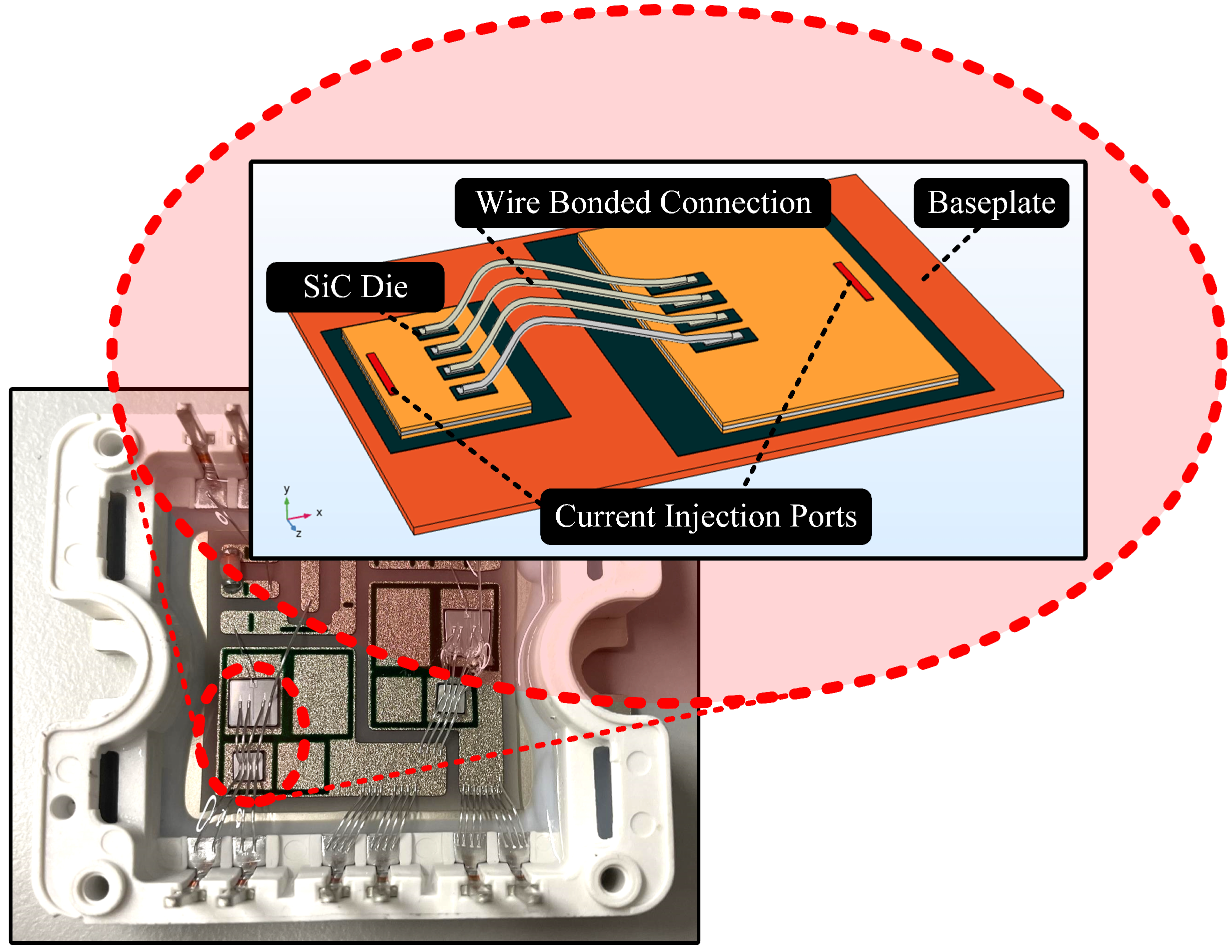
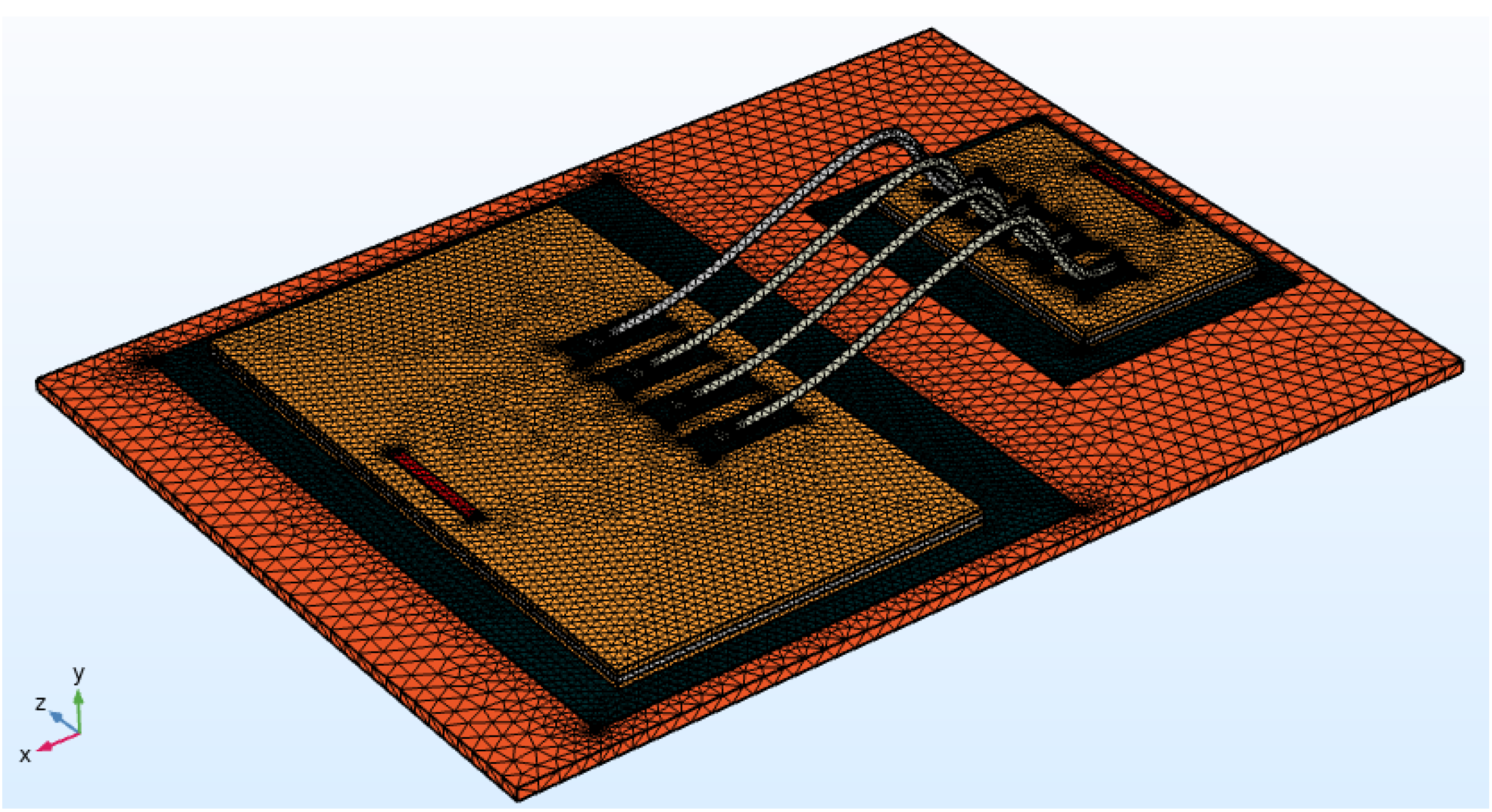
To study power cycling-related wear-out mechanisms, the layered-based structure of the case study SiC MOSFET power module (1200 V/55 A, MSCSM120AM50CT1AG, manufactured by Microsemi [29]) is simulated in COMSOL Multiphysics, as shown in Figure 5. The concentration of this paper is on the magnetic field profile in the wire bonded connection of the power module, and hence, to improve the simulation speed, only the WB-based connection of the SiC MOSFET and diode chips are simulated in the developed 3D FEM model, as shown in Figure 5. It is because of the fact that this area of the power module has been introduced as the most vulnerable area against degradation [2]. By this method, the mesh size of the FEM model (see Figure 6) is more efficiently built. With the curvature factor of 0.5, values of 0.65 mm and 0.08 mm are considered as the maximum and minimum element size of the assigned mesh. The employed materials’ specifications in developing the FEM model are listed in Table 1. Magnetic Field (mf) physics is used to obtain magnetic field pattern. Ampere’s law, magnetic insulation, initial values, and coil are the considered boundary conditions in the developed FEM model. The electrical current of each WB is controlled by coil boundary condition. Two ports, as the current injection ports, are considered on the two sides of the simulated topology. The external DC/DC Boost converter circuitry (shown in Figure 1) is simulated in PLECS. The circuit specifications of the simulated DC/DC converter are similar to the implemented one in Section 4.2. The instantaneous current value is inserted into COMSOL via the data interaction center to obtain the current distribution pattern based on the injected current value.
3. Magnetic Field Sensing
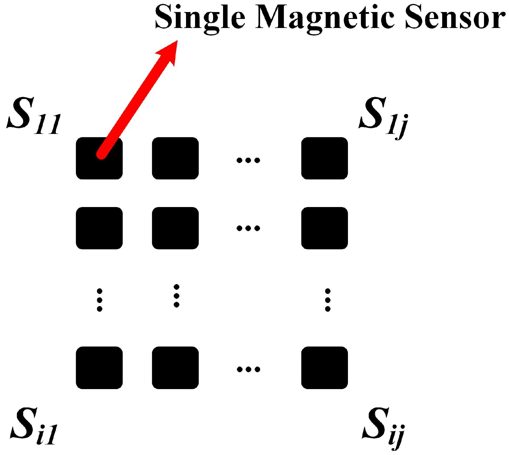
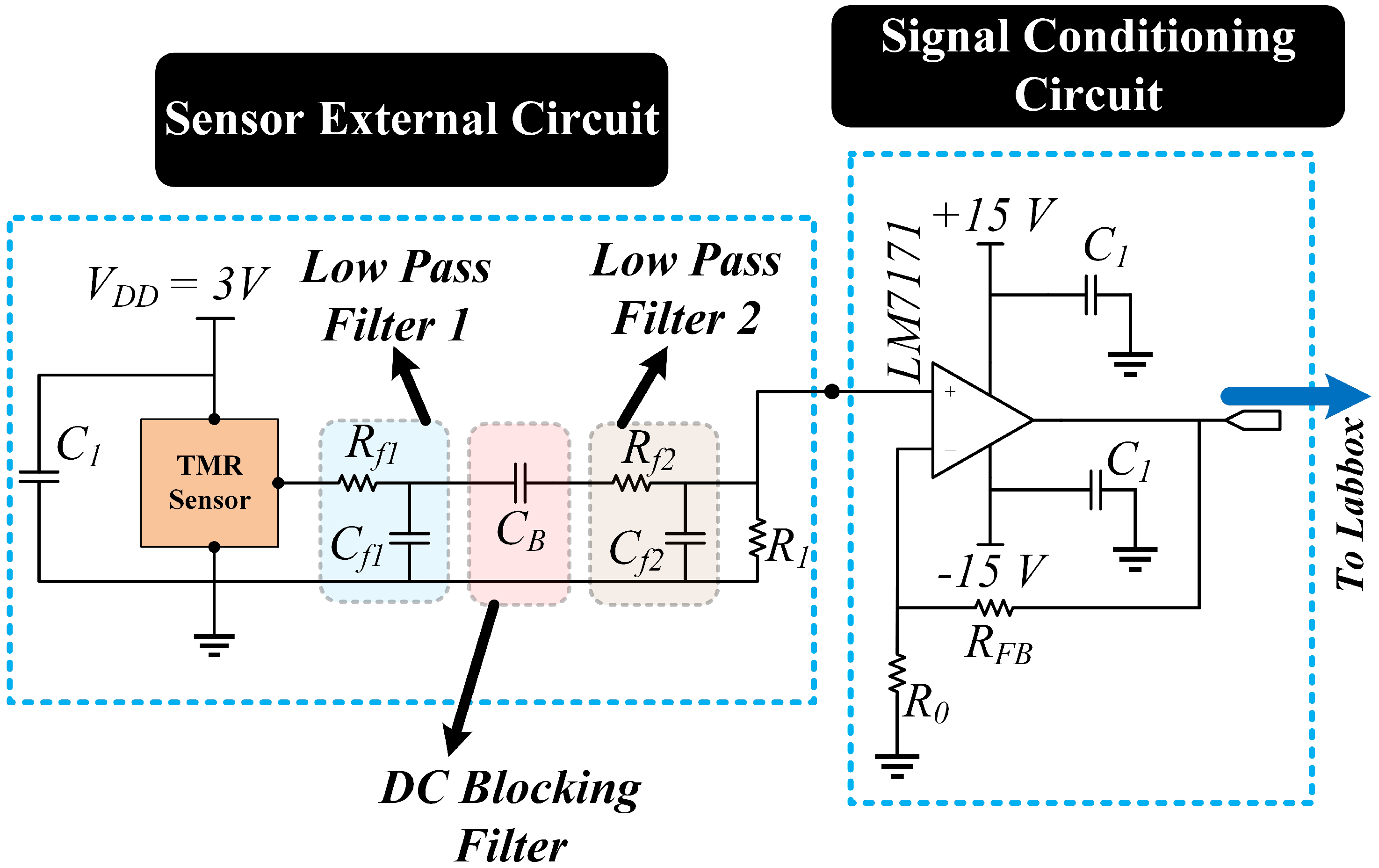
In a wire bonded connection with j single WBs, a sensor array is required for current distribution monitoring. In Figure 7, an overall diagram of the magnetic sensor array is shown. There will be i sensors along the WB direction and on its top area. The average value of these sensors is considered in current conduction capability of the WB. This gives more reliability to the developed sensing system. The output of the TMR magnetic field sensor contains a noise profile. To reduce high-frequency noise, based on (9), we designed two cascaded low pass filters to filter out possible sensor output noise.
In (9), , and are the cut-off frequency, resistance and capacitance values in the low pass filter circuit. As the TMR sensor-based system is designed to measure electrical current waveforms of up to 50 kHz, the cut-off frequency in this design is set at 100 kHz. Assuming k, capacitance of the filter is obtained as pF. In Figure 8, the external circuitry of the sensor is shown. The DC output value of the sensor output is filtered using pF as a capacitive DC blocking filter to bypass the probability of saturation in the signal conditioning circuit and HIL. Another low pass filter, consisting of k and pF, is used to eliminate the effect of oscillation of on the output signal of the sensor.
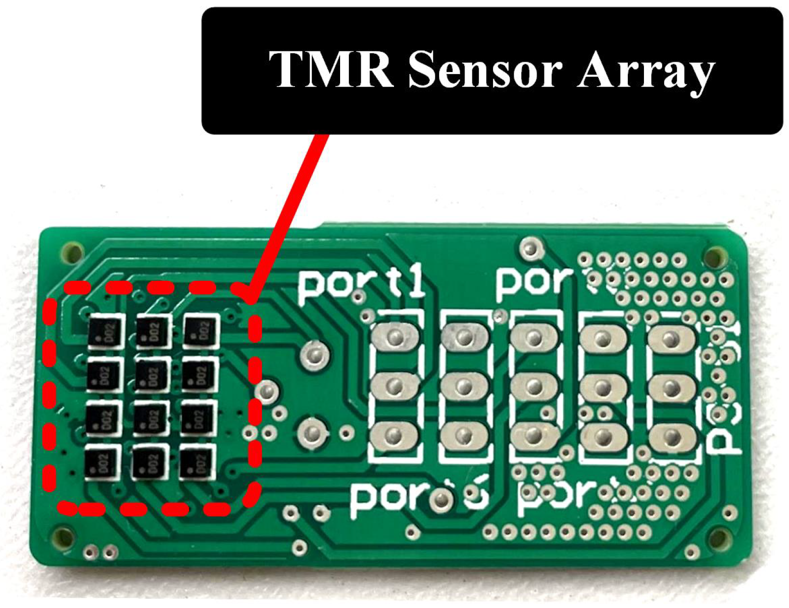
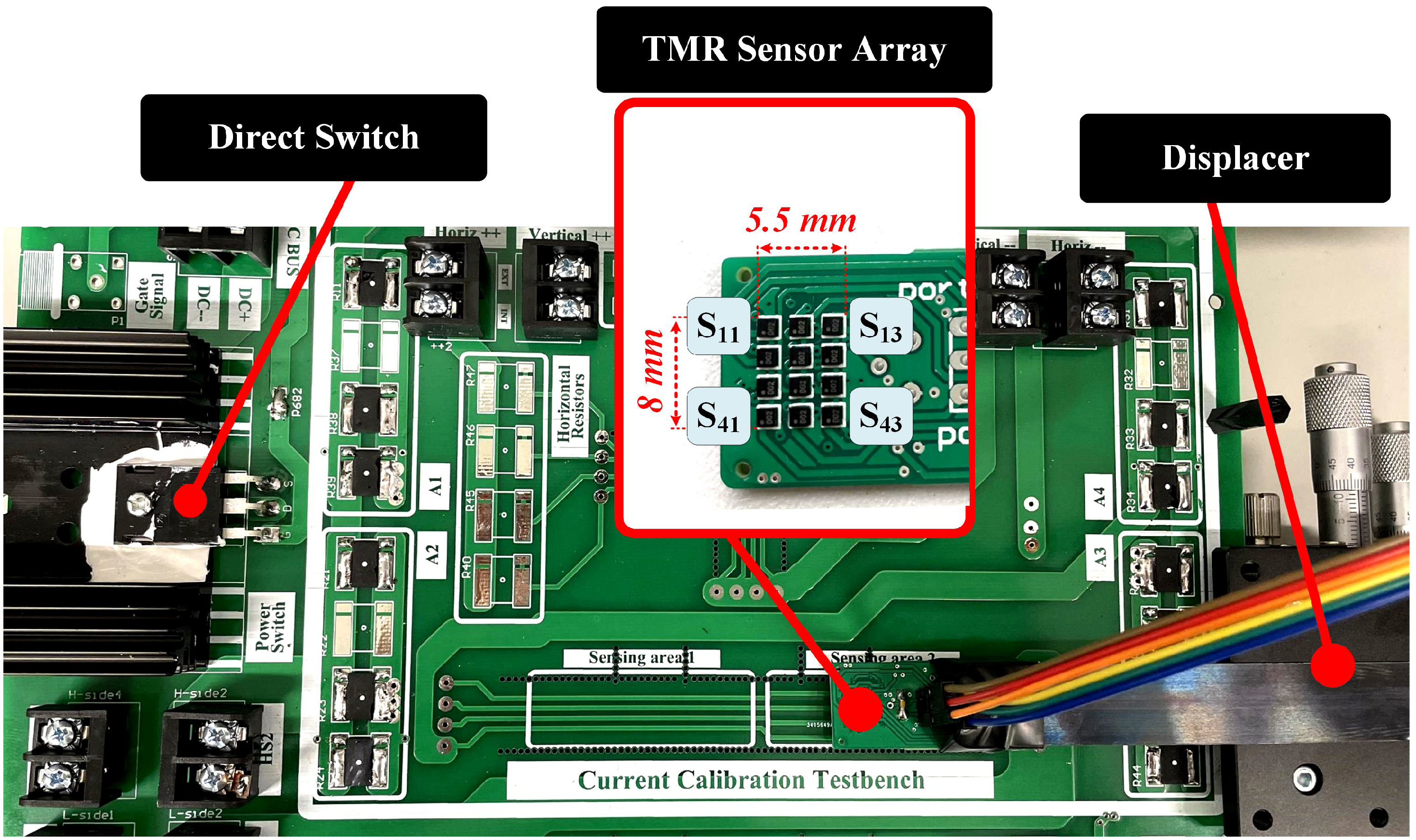
We discussed (cf. Section 1) that the developed sensing system of the proposed CM technique must be able to detect a minimum 5% change in the WB current value, used as the required sensitivity of the magnetic sensing system. Moreover, considering the limitations in the available upper area of the wire bonded connection, the mechanical dimensions of the employed sensors are facing limitations in the available space as well. We use RR111-1DC2-332 TMR sensor [30], manufactured by Coto Technology, with LGA-4 package (dimensions: 1.4 mm × 1.4 mm × 0.45 mm) and sensitivity of 200 mV/V/mT. A 4 × 3 sensor array is designed as shown in Figure 9, and to achieve the highest sensitivity, the supply voltage of the sensor () is set on 3 V, which leads to having a 600 mV/mT sensitivity. The shown sensor array in Figure 9. is designed for capturing the magnetic field above the four WBs in the case study power module. On each WB, three sensors will be placed, and the second sensor in each raw is placed on the center of the hyperbola shape of the WB. All the dimensions in the implemented sensor array are based on the dimensions of the case study power module WB connection.
3.1. Magnetic Sensor Board Calibration
To monitor the current of the WBs with the required level of precision and accuracy, the order of 0.1 G change must be observable in sensor readings. This means that for a sensor with the sensitivity of 200 mV/V/mT and V, the overall change of the sensor’s output voltage must be in 6 mV range. Therefore, sensor calibration and a preliminary evaluation of the developed magnetic sensor array are required for accurate sensor readings of current anomalies among multiple current paths. The calibration of the developed magnetic sensor board is carried out in two steps:
3.1.1. Individual Calibration of Sensors
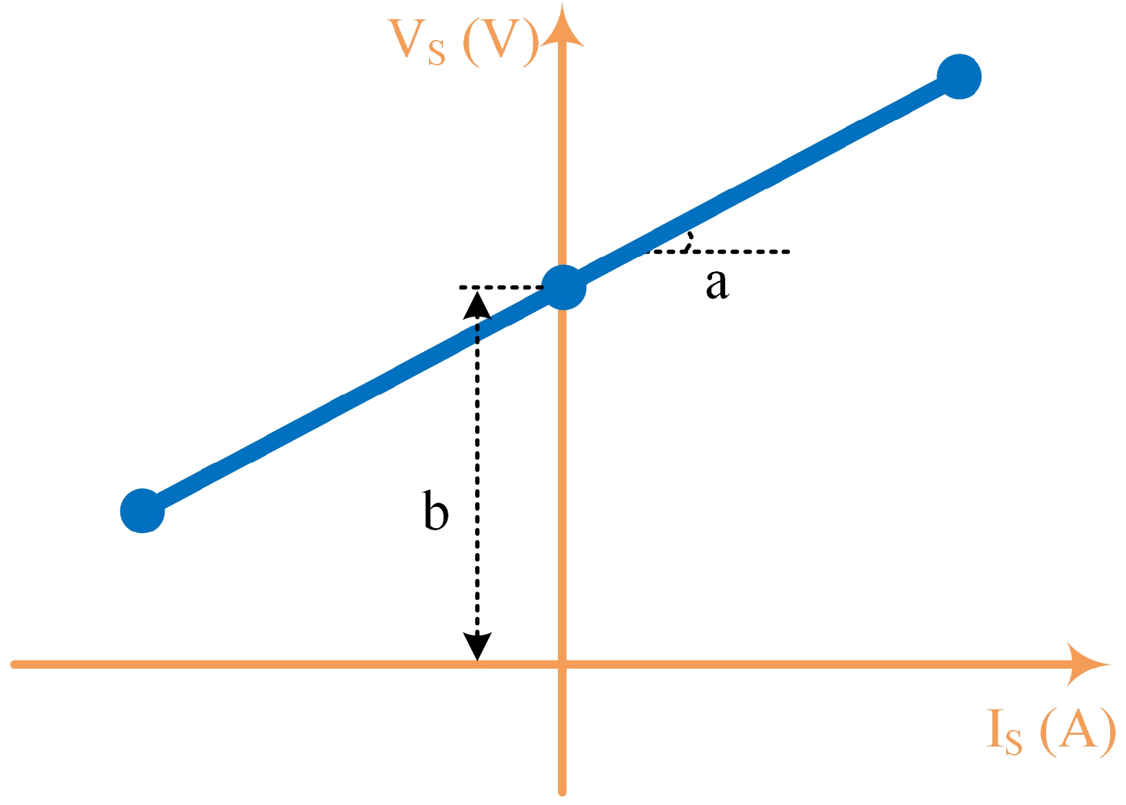
Based on the sensed current value (), the magnetic sensor output voltage () follows a straight line, i.e., transfer line, as (10). In Figure 10, the sensor transfer line, offset value (b), and voltage gain value (a) are shown.
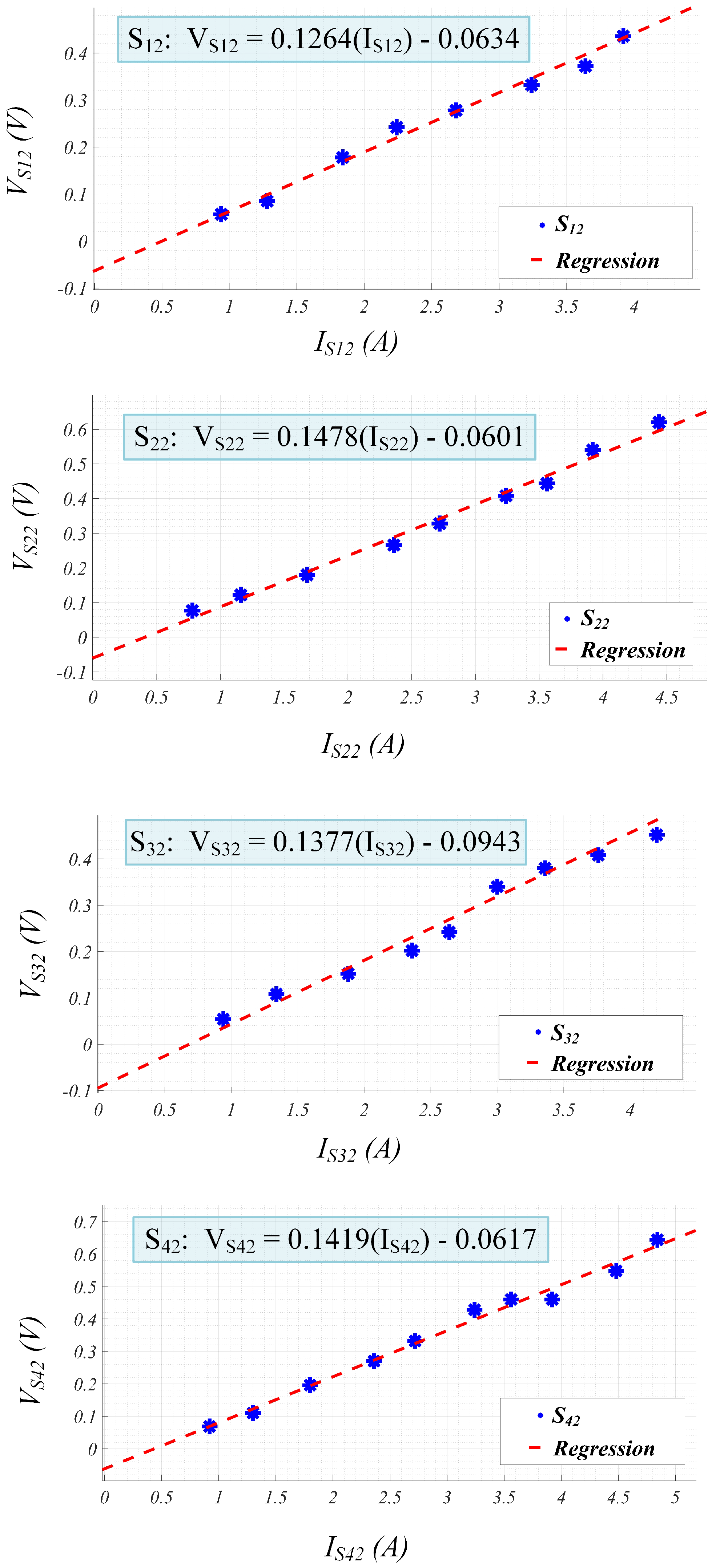
Ideally, both a and b coefficients can be calculated based on the sensor’s operational parameters such as sensitivity and offset voltage. Any deviations from this transfer line are considered as sensor errors. Due to manufacturing and semiconductor packaging processes, a percentage error is considered for the sensor sensitivity in the datasheet, which is about 12% for the employed TMR sensors used in our case. To bypass the errors, the transfer line of an individual sensor is obtained separately by applying a range of current values with the switching frequency of 40 kHz. A 1-D regression is applied for the sensor acquired data, and the transfer line of each sensor is obtained. In Figure 11, the individual sensor calibration is shown for , , , and , which are the four TMR sensors on top of the WB2 at the hyperbola-shape center of it. is the output voltage of , and is the value of the electrical current of the corresponding WB.
3.1.2. Calibration for Current Anomaly Detection
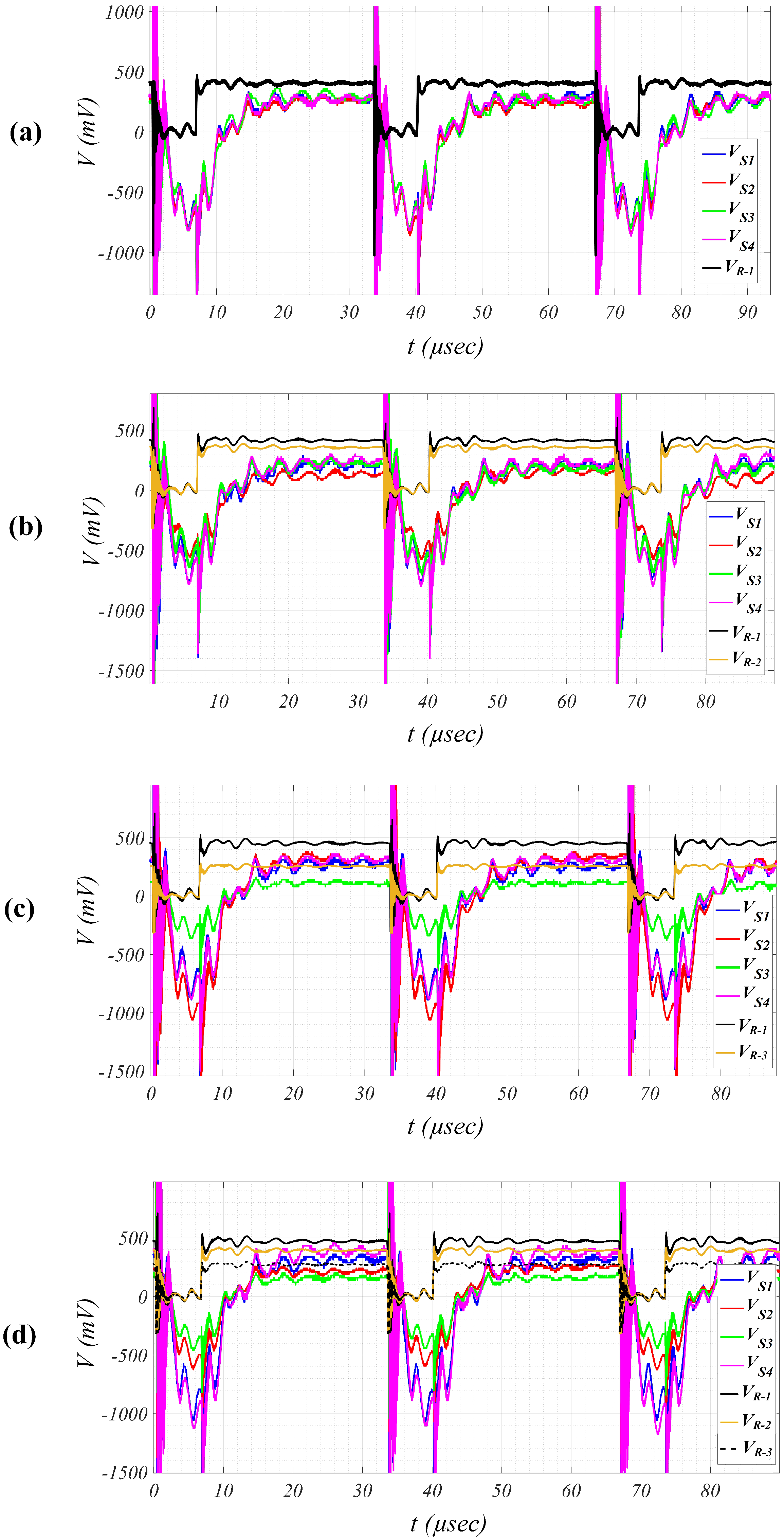
Depending on the WB fatigue level, the overall change in the measured magnetic field value of the wire bonded connection is in the range of 5% to 30% in a single or multiple WBs. Therefore, the developed magnetic field sensing should be capable of sensing the current anomalies in the range of 5% of the nominal WB current in the normal condition. For experimental examination, a resistive-based current sharing PCB board, capable of sharing a specific amount of current between four current paths is implemented. In Figure 12 and Figure 13, the circuit diagram and the PCB implementation of this resistive-based current sharing technique are shown respectively. In each of the resistive stacks, e.g., , , , and , four paralleled high precision current sensing type metal strip resistors (80 m, 2 W) are used. The track lengths of all the paths are equal to bypass the resistance and inductance effects of the track itself. Therefore, the path resistance of each track can be adjusted precisely by setting each stack’s overall resistance. Four current distribution conditions are considered in this section: (1) normal condition; (2) 20% reduction in path No.1 current conduction capability; (3) 80% reduction in path No.3 current conduction capability; (4) 20% reduction in path No.1 and 80% reduction in path No.3 current conduction capabilities.
For path No. i, the average of the three sensors on top of the WB (, , and ) is shown as in Figure 14. For the tracks with reduced current conduction capability, a resistive current measurement is also used, which is shown by for ith track in Figure 14.
As seen, peak to peak value is changed from 1100 mV in normal operation to 742 mV in 20% faulty operation, e.g., 358 mV change, which means 7% deviation from the expected sensor output based on the obtained transfer line. The difference is related to the effect of the magnetic field of the adjacent paths. Besides, as the overall current of the connection is constant, a 180 mV increment is seen in the sensor output voltages of the other sensors on the top of healthy paths.
4. Failure Onset Detection
In this section, the detection of the current distribution anomaly is validated experimentally. In Section 4.1, the current distribution behaviour in various WB-related failure mechanisms is studied using the developed simulation platform (cf. Figure 4). Moreover, based on the degraded power modules, the proposed CM technique using the developed magnetic field sensing system (cf. Section 3) will be validated in the HIL experimental set-up.
4.1. Simulation Verification
Regarding the major WB failure mechanisms, three scenarios are considered for the switch WB failure. Each scenario is simulated and tested separately.
Scenario 1, WB cracking: This mechanism usually occurs in the power cycling with short dwelling time between the heating phase and the cooling phase [17]. The heel cracking process occurs in the die area. The formed cracks are acting as the onset of complete WB lift-off. In this paper, to simulate this class of degradation, a cuboid area in the die attach area of the WB is considered (see Figure 15). Based on [2], the electrical conductivity of the inserted area is considered as 70% of the normal non-degraded value. WB2 is chosen as the faulty WB in this scenario.
Scenario 2, WB partial lift-off: This mechanism usually occurs in the fast power cycling conditions [18]. With each lifted WB, the current is conducted through a smaller surface, resulting in local overheating and significant mechanical stress in the SiC chip [17]. The first WB lift-off is reported for the WBs on the outer side areas of the chip [18]. In other words, the WBs on two outer sides of the connection are more probable to experience a lift-off due to the degradation. WB4, as an outer side WB, is considered as the degraded one in this scenario.
Scenario 3, WB complete lift-off: In some WB connections with a large number of WBs, a sudden lift-off of one or two WBs has been reported [17,18]. The complete lift-off results in a step increment in the current of other WBs, leading to more temperature stress on the remaining WBs [2]. WB3 is chosen as the complete lifted-off WB in this scenario.
The current distribution between the four WBs of the case study power module is reported in Table 2. As expected, the lowest change in the current value is reported in scenario 1, while the highest change occurred in scenario 3 in comparison to the normal operation.
4.2. Experimental Verification
The proposed magnetic field-based CM technique is tested for the case study power module in a DC/DC Boost converter topology. In Figure 1 and Table 3, the circuit schematic and the overall ratings of the implemented power circuit are shown respectively. Regarding the employed load on the output of the implemented DC/DC converter, the switch current is in the range of average value of 21 A. From electrical point of view, the employed power modules in the experimental verification process should have the nominal current value in the range of 35 A to 50 A. From mechanical point of view, the employed power module should have wire bonded-based connections in the power connection. It is also preferred to use a power module with easy access to the top area of the WB connection.
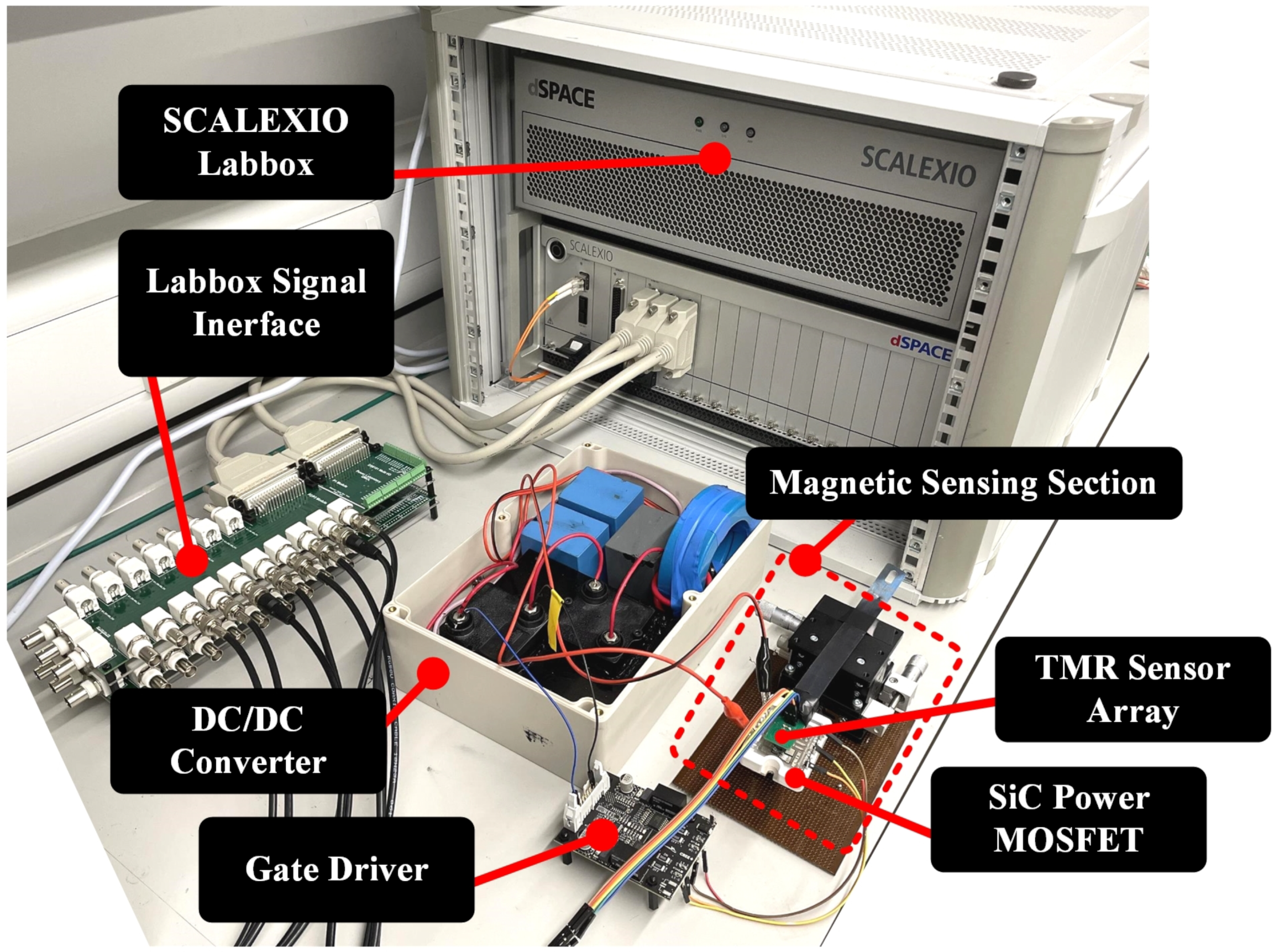
In Section 3, the design of the sensor array was described in detail. The sensor readings (output signals) are transferred to a real-time simulator, dSPACE SCALEXIO, in a Hardware In the Loop (HIL) set-up to run the condition monitoring system (see Figure 16).
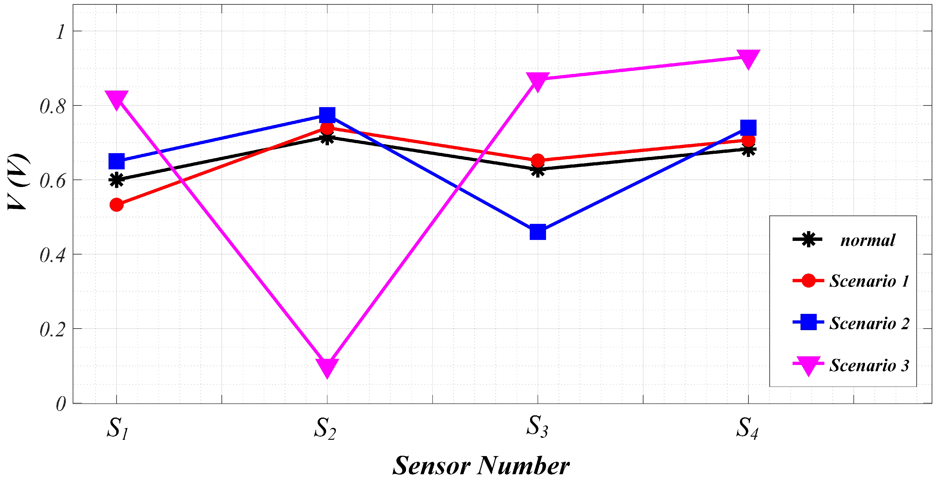
To evaluate the CM performance, the three simulation scenarios (cf. Section 4.1) are applied to the power module. The output of the sensor array is shown in Figure 17. represents the average value of the three sensors on one specific WB.
4.3. Discussion
Scenario 1 (WB cracking): To mimic this mode of degradation, the connection of WB1 to the die area is affected using a heating source. As a result, the SiC chip and the WB connection at the die area are changed in their thermal characteristics, leading to a reduction in electrical contact on the die area of the switch. In Figure 17, it is shown that the average value of the three corresponding TMR sensors of WB1 has changed from 600 mV to 530 mV (11.7% reduction). The current values of WB2, WB3, and WB4 have been increased 3.9%, 4.1%, and 3.2% respectively.
Scenario 2 (partial WB lift-off): WB3 attachment to the die area is partially detached by using a mechanical tool. It has led to a have a change in the output of TMR sensors on top of WB3 from 650 mV to 460 mV (29.4% reduction). 12.8%, 8.3%, and 8.7% changes are observed in sensor output values of WB1, WB2, and WB4 respectively.
Scenario 3 (complete WB lift-off): this scenario is imitated by cutting off WB2. The results in Figure 17. shows that the corresponding sensor value has changed from 730 mV to 100 mV (86% reduction). 30.2%, 33%, and 29.1% changes are observed in WB1, WB2, and WB4 sensor output values respectively.
Depending on the degradation type, it was shown that the percentage change in the corresponding sensor of the faulty WB is in the range of 11.7% to 86%. As the sensing system is fully isolated from the power circuit, thermo-mechanical cycling and degradation effects are so minor in the TMR sensors, and hence, the sensor transfer line is less probable to be altered. Besides, a value change in the range of 3.2% to 33% was detected in the corresponding sensors of the other WBs. This shows that in case of probable malfunctioning of a sensor, the change in the adjacent sensors’ outputs can also show the current anomaly occurrence in the wire bonded connection.
5. Conclusions
A novel package-related failure indicator was presented in this paper and validated using a SiC MOSFET power modules in a DC/DC Boost converter circuit. We proposed to monitor the current distribution in specific wire bonded connection of the power module using a dedicated state-of-the-art TMR sensor array. A calibration methodology was further designed to guarantee the accuracy of the sensor output in high frequency SiC applications with up to 50 KHz. It was shown via experimental testing that a minimum 5% change in the nominal value of the wire bond current can be detected as a failure onset. Although the proposed CM technique is based on a fully isolated configuration in the sensing section to bypass the effect of EMI and other high voltage-related issues, evaluation in high voltage set-up should be carried out in future works as an enabling verification for employing the proposed CM technique in high reliability power electronic applications such as electric vehicles and wind turbines.
Author Contributions
Conceptualization, J.N. and K.M.; methodology, J.N. and M.P.F.; software, J.N.; validation, J.N. and K.M.; formal analysis, J.N. and M.P.F.; investigation, J.N.; resources, J.N.; writing—original draft preparation, J.N.; writing—review and editing, K.M. and M.P.F.; visualization, J.N.; supervision, K.M. and M.P.F.; project administration, K.M.; funding acquisition, K.M. All authors have read and agreed to the published version of the manuscript.
Funding
This research is funded by the school of electronics engineering and computer science (EECS) at the Queen Mary University of London, London, UK.
Institutional Review Board Statement
Not applicable.
Informed Consent Statement
Not applicable.
Data Availability Statement
The data presented in this study are available on request from the corresponding author.
Conflicts of Interest
The authors declare no conflict of interest.
References
- Chen, W.; Zhang, L.; Pattipati, K.; Bazzi, A.M.; Joshi, S.; Dede, E.M. Data-Driven Approach for Fault Prognosis of SiC MOSFETs. IEEE Trans. Power Electron. 2020, 35, 4048–4062. [Google Scholar] [CrossRef]
- Ni, Z.; Lyu, X.; Yadav, O.P.; Singh, B.N.; Zheng, S.; Cao, D. Overview of Real-Time Lifetime Prediction and Extension for SiC Power Converters. IEEE Trans. Power Electron. 2020, 35, 7765–7794. [Google Scholar] [CrossRef]
- Naghibi, J.; Mehran, K.; Foster, M.P. An Online Failure Assessment Approach for SiC-based MOSFET Power Modules Using Iterative Condition Monitoring Technique. In Proceedings of the 2020 IEEE 21st Workshop on Control and Modeling for Power Electronics (COMPEL), Aalborg, Denmark, 9 November 2020; pp. 1–5. [Google Scholar] [CrossRef]
- Ziegler, S.; Woodward, R.C.; Iu, H.H.; Borle, L.J. Current Sensing Techniques: A Review. IEEE Sens. J. 2009, 9, 354–376. [Google Scholar] [CrossRef]
- Ugur, E.; Yang, F.; Pu, S.; Zhao, S.; Akin, B. Degradation assessment and precursor identification for SiC MOSFETs under high temp cycling. IEEE Trans. Ind. Appl. 2019, 55, 2858–2867. [Google Scholar] [CrossRef]
- Chen, M.; Wang, H.; Pan, D.; Wang, X.; Blaabjerg, F. Thermal characterization of silicon carbide mosfet module suitable for high-temperature computationally-efficient thermal-profile prediction. IEEE J. Emerg. Sel. Top. Power Electron. 2020, 9, 3947–3958. [Google Scholar] [CrossRef]
- Gothner, F.; Spro, O.C.; Herncs, M.; Peftitsis, D. Challenges of SiC MOSFET Power Cycling Methodology. In Proceedings of the 2018 20th European Conference on Power Electronics and Applications (EPE’18 ECCE Europe), Riga, Latvia, 17–21 September 2018; pp. 1–8. [Google Scholar]
- Gonzalez-Hernando, F.; San-Sebastian, J.; Garcia-Bediaga, A.; Arias, M.; Iannuzzo, F.; Blaabjerg, F. Wear-Out Condition Monitoring of IGBT and mosfet Power Modules in Inverter Operation. IEEE Trans. Ind. Appl. 2019, 55, 6184–6192. [Google Scholar] [CrossRef]
- Ceccarelli, L.; Kotecha, R.; Iannuzzo, F.; Mantooth, A. Fast Electro-thermal Simulation Strategy for SiC MOSFETs Based on Power Loss Mapping. In Proceedings of the 2018 IEEE International Power Electronics and Application Conference and Exposition (PEAC), Shenzhen, China, 4–7 November 2018; pp. 1–6. [Google Scholar]
- Gonzalez, J.O.; Alatise, O.; Hu, J.; Ran, L.; Mawby, P.A. An investigation of temperature-sensitive electrical parameters for SiC power MOSFETs. IEEE Trans. Power Electron. 2016, 32, 7954–7966. [Google Scholar] [CrossRef] [Green Version]
- Griffo, A.; Wang, J.; Colombage, K.; Kamel, T. Real-Time Measurement of Temperature Sensitive Electrical Parameters in SiC Power MOSFETs. IEEE Trans. Ind. Electron. 2018, 65, 2663–2671. [Google Scholar] [CrossRef] [Green Version]
- Guo, W.; Fu, G.; Wan, B.; Su, Y. Reliability Assessment Methodology of Power Devices Based on Physics of Failure and Multivariate Copulas. In Proceedings of the 2019 Prognostics and System Health Management Conference (PHM-Qingdao), Qingdao, China, 25–27 October 2019; pp. 1–6. [Google Scholar]
- Zhang, Z.; Dyer, J.; Wu, X.; Wang, F.; Costinett, D.; Tolbert, L.M.; Blalock, B.J. Online junction temperature monitoring using intelligent gate drive for SiC power devices. IEEE Trans. Power Electron. 2018, 34, 7922–7932. [Google Scholar] [CrossRef]
- Stella, F.; Pellegrino, G.; Armando, E.; Daprà, D. Online junction temperature estimation of SiC power MOSFETs through on-state voltage mapping. IEEE Trans. Ind. Appl. 2018, 54, 3453–3462. [Google Scholar] [CrossRef]
- Volke, A.; Hornkamp, M. IGBT Modules: Technologies, Driver and Application; Infeneon Technologies: Neubiberg, Germany, 2011. [Google Scholar]
- Chan, T.; Chen, J.; Ko, P.; Hu, C. The impact of gate-induced drain leakage current on MOSFET scaling. In Proceedings of the 1987 International Electron Devices Meeting, Washington, DC, USA, 6–9 December 1987; pp. 718–721. [Google Scholar]
- Baba, S.; Gieraltowski, A.; Jasinski, M.; Blaabjerg, F.; Bahman, A.S.; Zelechowski, M. Active Power Cycling Test Bench for SiC Power MOSFET s—Principles, Design, and Implementation. IEEE Trans. Power Electron. 2020, 36, 2661–2675. [Google Scholar] [CrossRef]
- Schilling, O.; Schäfer, M.; Mainka, K.; Thoben, M.; Sauerland, F. Power cycling testing and FE modelling focussed on Al wire bond fatigue in high power IGBT modules. Microelectron. Reliab. 2012, 52, 2347–2352. [Google Scholar] [CrossRef]
- Sokolov, A.; Liu, C.; Mohn, F. Reliability assessment of SiC power module stack based on thermo-structural analysis. In Proceedings of the 2018 19th International Conference on Thermal, Mechanical and Multi-Physics Simulation and Experiments in Microelectronics and Microsystems (EuroSimE), Toulouse, France, 15–18 April 2018; pp. 1–4. [Google Scholar] [CrossRef]
- Alvi, M.H.; Sheng, M.; Lorenz, R.D.; Jahns, T.M. SiC Power Module Design for High Bandwidth Integrated Current Sensing using a Magnetoresistive Point Field Detector. In Proceedings of the 2020 IEEE Applied Power Electronics Conference and Exposition (APEC), New Orleans, LA, USA, 15–19 March 2020; pp. 1506–1512. [Google Scholar]
- Nibir, S.J.; Parkhideh, B. Magnetoresistor with planar magnetic concentrator as wideband contactless current sensor for power electronics applications. IEEE Trans. Ind. Electron. 2017, 65, 2766–2774. [Google Scholar] [CrossRef]
- Nibir, S.J.; Biglarbegian, M.; Parkhideh, B. A Non-Invasive DC-10-MHz Wideband Current Sensor for Ultra-Fast Current Sensing in High-Frequency Power Electronic Converters. IEEE Trans. Power Electron. 2019, 34, 9095–9104. [Google Scholar] [CrossRef]
- Shao, S.; Yu, N.; Xu, X.; Bai, J.; Wu, X.; Zhang, J. Tunnel Magnetoresistance-Based Short-Circuit and Over-Current Protection for IGBT Module. IEEE Trans. Power Electron. 2020, 35, 10930–10944. [Google Scholar] [CrossRef]
- Nasab, J.N.; Hadizade, A.; Mohsenzade, S.; Zarghany, M.; Kaboli, S. A Marx-based generator with adjustable FWHM using a controllable magnetic switch. IEEE Trans. Dielectr. Electr. Insul. 2019, 26, 324–331. [Google Scholar] [CrossRef]
- Miranda, J.A. Magnetic field calculation for arbitrarily shaped planar wires. Am. J. Phys. 2000, 68, 254–258. [Google Scholar] [CrossRef]
- Griffiths, D. Introduction to Electrodynamics; Prentice-Hall: Upper Saddle River, NJ, USA, 1999. [Google Scholar]
- Jia, Y.; Xiao, F.; Duan, Y.; Luo, Y.; Liu, B.; Huang, Y. PSpice-COMSOL Based 3D Electro-Thermal-Mechanical Modeling of IGBT Power Module. IEEE J. Emerg. Sel. Top. Power Electron. 2019, 8, 4173–4185. [Google Scholar] [CrossRef]
- Naghibi, J.; Mehran, K. Multiphysics Condition Monitoring Technique for Reliability Assessment of Wide Bandgap-Based Power Modules in Electric Vehicle Application. In Proceedings of the 2020 Fifteenth International Conference on Ecological Vehicles and Renewable Energies (EVER), Monte-Carlo, Monaco, 10–12 September 2020; pp. 1–6. [Google Scholar] [CrossRef]
- Microsemi. 1200 V, 55 A Phase Leg SiC MOSFET Power Module. 2019. Available online: https://www.microsemi.com/document-portal/doc_download/1244785-mscsm120am50ct1ag-datasheet (accessed on 1 August 2021).
- Coto Technology. Analog, TMR RedRock® RR111. 2019. Available online: https://media.cotorelay.com/wp-content/uploads/2018/02/03173949/RedRock-111TMR-Datasheet2.pdf (accessed on 1 August 2021).
Figure 1.
Proposed CM system of the SiC power MOSFETs.

Figure 2.
A single WB geometry with the hyperbola shape structure.

Figure 3.
Mutual effect of the adjacent WBs in the sensed magnetic field of WB2.

Figure 4.
Developed simulation platform and the data interaction between the three main subsections.
Figure 4.
Developed simulation platform and the data interaction between the three main subsections.

Figure 5.
3D FEM model of the case study 1200 V/55 A SiC MOSFET power module in the wire bonded connection area.
Figure 5.
3D FEM model of the case study 1200 V/55 A SiC MOSFET power module in the wire bonded connection area.

Figure 6.
Assigned mesh for the 3D structure of the switch in FEM solutions.

Figure 7.
Magnetic sensor array.

Figure 8.
External magnetic sensor circuitry and the signal conditioning section.

Figure 9.
4 × 3 implemented TMR sensor array.

Figure 10.
Sensor output transfer line.

Figure 11.
Individual calibration of , , , and sensors in the sensor array.

Figure 12.
Resistive-based current sharing circuit for magnetic sensor calibration.

Figure 13.
PCB implementation of calibration set-up and the employed sensor array board.

Figure 14.
Sensor array calibration in four different current sharing conditions, (a) normal condition, (b) 20% reduction in path No.1 current conduction capability, (c) 80% reduction in path No.3 current conduction capability, and (d) 20% reduction in path No.1 and 80% reduction in path No.3 current conduction capabilities.

Figure 15.
Scenario 1 failure simulation in 3D FEM model.

Figure 16.
Experimental set-up of the proposed CM technique.

Figure 17.
Sensor outputs of the normal condition and three implemented scenarios.


Table 1.
Material specifications in the developed FEM model of SiC MOSFET power module.
| Material | Thermal Conductivity | Heat Capacity | Density |
|---|---|---|---|
| [W/(m·K)] | [J/(kg·K)] | [kg/m] | |
| Aluminium () | 239 | 910 | 2699 |
| Copper () | 385 | 380 | 180 |
| Silicon Carbide () | 353 | 1031 | 3211 |
| Solder () | 60 | 160 | 7400 |
| Ceramic () | 27 | 776 | 3900 |
| Silicon gel | 0.2 | 900 | 1250 |
Table 2.
Simulation results of the current distribution in wire bonded connection of the power module.
Table 2.
Simulation results of the current distribution in wire bonded connection of the power module.
| Condition | |||||
| Normal | 21 | 5.25 | 5.25 | 5.25 | 5.25 |
| Scenario 1 | 21 | 5.39 | 4.81 | 5.39 | 5.39 |
| Scenario 2 | 21 | 5.49 | 5.49 | 5.49 | 4.47 |
| Scenario 3 | 21 | 7 | 7 | 0 | 7 |
Table 3.
Implemented DC/DC Boost converter circuit specifications.
| Parameter | Value |
| 31 V | |
| 49 V | |
| L | 100 H |
| 55 F | |
| 100 F | |
| 50 kHz | |
| 470 W |
Publisher’s Note: MDPI stays neutral with regard to jurisdictional claims in published maps and institutional affiliations. |
© 2021 by the authors. Licensee MDPI, Basel, Switzerland. This article is an open access article distributed under the terms and conditions of the Creative Commons Attribution (CC BY) license (https://creativecommons.org/licenses/by/4.0/).
Share and Cite
MDPI and ACS Style
Naghibi, J.; Mehran, K.; Foster, M.P. High-Frequency Non-Invasive Magnetic Field-Based Condition Monitoring of SiC Power MOSFET Modules. Energies 2021, 14, 6720. https://doi.org/10.3390/en14206720
AMA Style
Naghibi J, Mehran K, Foster MP. High-Frequency Non-Invasive Magnetic Field-Based Condition Monitoring of SiC Power MOSFET Modules. Energies. 2021; 14(20):6720. https://doi.org/10.3390/en14206720
Chicago/Turabian StyleNaghibi, Javad, Kamyar Mehran, and Martin P. Foster. 2021. "High-Frequency Non-Invasive Magnetic Field-Based Condition Monitoring of SiC Power MOSFET Modules" Energies 14, no. 20: 6720. https://doi.org/10.3390/en14206720
Note that from the first issue of 2016, this journal uses article numbers instead of page numbers. See further details here.