Influence of Insulating Material Properties on Partial Discharges at DC Voltage


Department of Electrical and Power Engineering, AGH University of Science and Technology, al. Mickiewicza 30, 30-059 Kraków, Poland
Energies 2020, 13(17), 4305; https://doi.org/10.3390/en13174305
Submission received: 18 July 2020
/
Revised: 17 August 2020
/
Accepted: 19 August 2020
/
Published: 19 August 2020
(This article belongs to the Section F: Electrical Engineering)
Abstract
:Understanding a partial discharge mechanism at direct current (DC) is an actual research topic that requires both modeling, simulations and measurements. This paper describes an influence of insulating material properties on partial discharges at DC voltage. Modifications of the traditional model reflecting the conditions of partial discharges (PD) inception and post discharge processes at DC voltage have been proposed. The aim was to show the partial discharge mechanisms and draw attention to the role of parameters of insulation materials adjacent to the cavity at DC voltage. The investigations were performed on two kinds of dielectric material used in power cables. Various combinations of specimens were designed to reveal the effect of the material resistivity on the PD activity. Key observations referred to the impact of the void adjacent material resistance on the partial discharge inception voltage threshold at DC voltage. The modified PD model was applied to analyze both inception and post discharge recovery stage. The role of dielectric properties of material adjacent to the void was investigated, highlighting its impact during static inception stage and in charging stage. Despite many simplifications introduced in the model, measurement results have confirmed the role of the dielectric material surrounding the void on partial discharge dynamics. The average time interval between PD pulses revealed a systematic relationship with respect to the applied voltage and specimen resistivity. This value can be considered in the future research for diagnostic indicator at DC voltage.
1. Introduction
The use of DC voltage in high voltage transmission systems is currently undergoing a renaissance. In fact, this applies to all voltage levels. On one side it refers to the highest voltage level and future HVDC (high voltage direct current) grids, not only peer-to-peer but also meshed ones. On the other side, enhancements in power electronics technologies have resulted in a broad interest in DC, also at medium and low voltage levels. Today DC systems are regularly observed in applications such as traction, e-mobility or solar converters and are more and more analyzed in power distribution solutions. The above elements imply interest in a design of reliable insulation of high voltage power equipment. Phenomena occurring in insulation in a strong electric field result in aging and include ionization processes in the dielectric materials. The DC insulation is a crucial element of high voltage power equipment, such as cables, transformer bushings, converter transformers—especially the valve winding, capacitors, including DC capacitors in HVDC modules; wall bushings [1,2,3,4]. The problem of the reliability of electrical power devices refers—in both AC and DC systems—to the possibility of assessing the condition of the insulation systems under the action of operational stresses.
One of the most reliable quality indicators of high voltage insulation systems is the measurement of partial discharges (PD). Partial discharges occur in high voltage, technical insulation systems causing deterioration and often during long term exposure are leading to a breakdown. The character of partial discharges in electrical insulation is dependent on the applied voltage waveform, resulting in different times, magnitudes and intensities of discharges for direct, alternating or impulse voltages. The mechanism of partial discharges is slightly different at AC and DC voltages. Many research studies over the last century have been dedicated to understanding that topic, however the majority was related to an alternating voltage.
This paper is focused on the partial discharges occurring at DC voltage and the influence of material resistivity, impacting the PD dynamics. The presented research aimed at developing assumptions for future diagnostic methods for assessing the state of insulation subjected to DC voltage. This experiments were carried out in laboratory tests using model specimens, containing partial discharge sources from distinct insulation materials. Insulation materials with different electrical parameters, in particular electrical resistivity, were used to assess the impact on the parameters of PD pulse sets recorded in the detection system. Investigations were performed on two materials used for power cable insulation, i.e., electrotechnical cellulose and polyethylene. The influence of those materials on the PD pulse repetition rate was discussed. Modifications of the traditional model reflecting the conditions of PD inception and post discharge processes at DC voltage have been proposed, as it is well known there is a difference in PD mechanism under AC and DC voltage. The first one is determined by material electrical permittivity, whereas the latter one by electrical resistivity. The first model of partial discharge mechanism, so-called “a-b-c” model, was introduced by Gemant and Philipphoff [5] almost a century ago. Originally, they investigated power losses in mass impregnated power cables caused by discharges in the cavities. This approach was further modified by Whitehead and Kreuger in the 1950s [6]. In this model the external detectable charge, commonly called apparent charge, is smaller than the real charge related to the place of discharge, which cannot be measured directly. The IEC60270 standard [7] is based on this concept. Some researchers [8,9,10] challenge this concept arguing that instead of capacitance determined by a void shape, the radius of discharge channel should be assumed. However, from the general perspective apart from the (a-b-c) capacitive model, in 80 ties of last century Pedersen [9] has introduce a dipole model based on electric field theory and dielectric flux density, which has been further elaborated by Lemke [8,10]. They criticized the network-based capacitive model, which was not fully reflecting the physics of gas discharges. In their concept the cavity is not discharged via a spark gap but rather charged due to the creation of charge carriers as a consequence of ionization processes in the gas filled cavity. Instantly after the discharge event, the charges of both polarities are deposited on the anode and cathode side of the void wall and a dipole moment is established, which induces charges on the electrodes (induced charge model). In this way a space charge field, often denoted as Eq (Poisson electric field), opposes the electrostatic field caused by the applied external test voltage (Laplacian electric field). In this approach, the current caused by the charge carriers in the void is moving through the solid dielectric column and results in a statement that the external charge detectable at the terminals of the test object must be equal to the internal charge, which is in contrast to the apparent charge concept. Another doubt of the “a-b-c” model based on capacitances questions the fact that there are no real “capacitor electrodes”, especially associated with a conventional capacitance. On the other side, it should be underlined that the “a-b-c” model has been very successfully used in PD modeling, simulations and theoretical considerations over many decades [11,12,13,14,15]. It can be concluded, analyzing both capacitive and dipole models, that external charge detectable at the terminals of a specimen or real power equipment is a quantity reflecting the PD severity or at least is proportional to the PD causing deterioration.
An unprecedented contribution to PD modeling was brought by Lutz Niemeyer at the beginning of 1990s, introducing a new approach that in many variations triggered PD-related simulation over the last three decades [16,17]. An important extension was the introduction of finite element modeling to PD simulations [18,19,20]. Thus, the third model used in this classification in partial discharge research is related to plasma physics. This model considers the plasma dynamics of the discharge and has been used for modeling dielectric barrier discharges. A well-established approach is to use drift diffusion equations that describe the dynamics of electrons, as well as positive and negative ions [21,22,23,24,25,26]. In that model, reflected and quantitatively described are such processes as impact ionization, attachment, recombination, diffusion and drift of charges. The coupled approach of fluid equations and Poisson equation allow to obtain temporal evolution of charge and electric field distribution within the void during the discharge development [27].
In the above context, in this paper the influence of material resistivity on partial discharges at DC voltage in cavities are studied using a modified “a-b-c” model. The analysis was focused on two aspects, i.e., static PD inception condition and post discharge recovery stage. The important novelty is to draw attention to the role of material resistance adjacent to the inclusion and interplay in the conditions for PD inception, as well as post PD void charging. As an indicator, the evolution of an average interval between the PD pulses in predefined measurement time was observed.
2. Partial Discharges at DC Voltage
It is known that progressive high voltage insulation deterioration caused by PD in gas-filled cavities (voids) is one of the major factors limiting the lifetime of power equipment. The quantity characterizing partial discharges in insulation systems at direct voltage is the number of impulses of discharges registered in the detection circuit at the predefined time period or the time interval between successive PD pulses. The conditions for initiating discharges in defects in the structure of insulation systems are determined—similarly to alternating voltage—by the value of the electric field strength necessary for ionization in the gas source of discharges. At steady-state of DC voltage, the distribution of the electric field strength in the insulated system is a resistive distribution. The above fact is the basis for the analysis of the discharge mechanism at direct voltage, including:
- ▪
- conditions of initiating discharges in gas inclusions in solid dielectrics, and
- ▪
- the impact of the properties of insulation materials on the quantities characterizing this phenomenon.
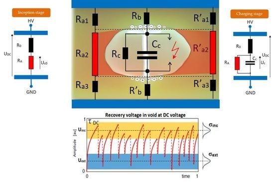
The main influence on the PD dynamics at DC has material resistivity, unlike its permittivity at AC. To analyze the static inception conditions at DC, the adopted “a-b-c” model is applied [5,28,29,30,31,32]. The investigations were performed on a model specimen reflecting one of the most typical defects in high voltage insulation. In a model shown in Figure 1, the resistors represent the material properties. In fact, relationships of those resistors are crucial for partial discharge inception voltage (PDIV, Uinc) calculations at DC.
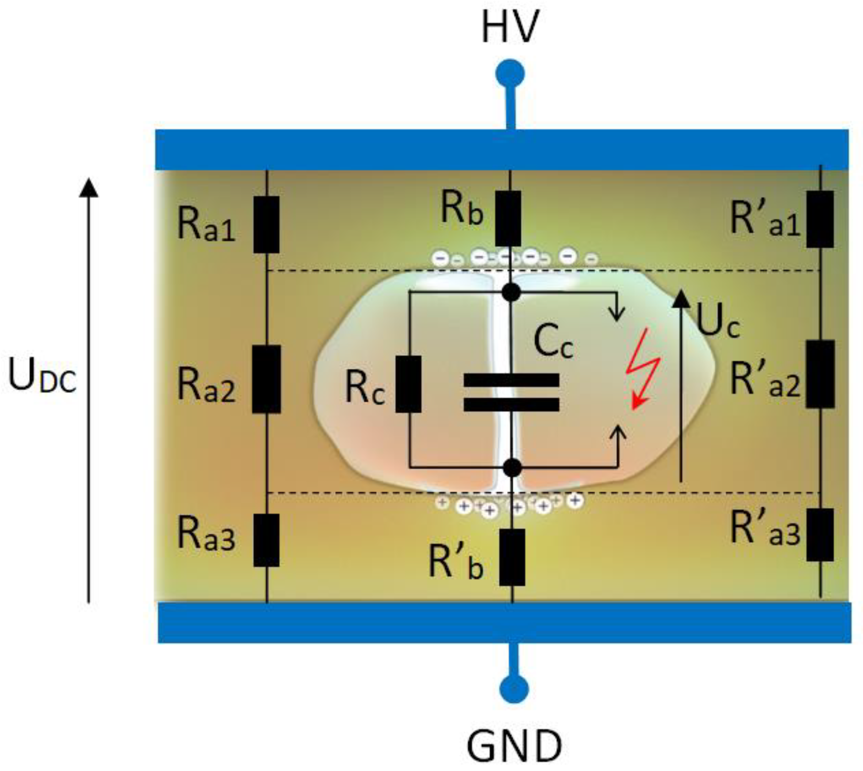
In the equivalent circuit (Figure 2), the source of the discharges represents the capacitance Cc and the resistance Rc. The air resistivity is very high, 1016 Ω·m at temperature 20 °C [33], hence in reality the resistance Rc, representing the gaseous void, is much higher than the resistance of solid dielectric, which is represented by Ra2 and R’a2. The indexed resistances Ra and Rb reflect the part of a homogeneous dielectric, free from discharges. In this representation (Figure 2a), the branch resistance Ra has been split according to the cavity profile, i.e., Ra2, R’a2 being parallel to the cavity (marked in red) and Ra1, R’a1, Ra3, R’a3 mimicking remaining parts. It is important to notice that usually the resistance Rc is much bigger than Ra2, R’a2, which are bypassing the resistance representing the gaseous void. The voltage build-up Uc required for PD inception corresponds to the voltage drop on resistance RA resultant from the combination of components Ra2 and R’a2. This is actually a very important novelty in modeling partial discharges occurrence at DC voltage. This effect is highlighted in Figure 2a, indicating the twofold effect of resistance RA.
At DC voltage two distinctive stages representing PD mechanism can be distinguished:
- (a)
- inception stage, when PD will occur, assuming fulfillment of all conditions,
- (b)
- charging stage, when post-discharge recovery occurs.
It is shown in this paper that the void material properties, such as resistivity, both volume and surface, are crucial in proper modeling of above mentioned stages. The first one is influencing the inception phase, whereas the latter one impacting the charging time.
Discharge stages in an air-filled cavity illustrate the simplified equivalent circuits:
- ▪
- inception stage (Figure 2b) will occur when voltage drop on the equivalent resistance RA reaches the PD inception voltage Uinc,
- ▪
- charging stage (Figure 2c): charge flow through volume resistance R0 and RA, including effects of void walls represented by surface resistance of RA, will result in recovery voltage Uc build-up on the capacitance CC.
(a) Static inception stage
Inception stage in this paper is analyzed mainly with respect to the required static inception electric field strength, i.e., other conditions such as availability of starting electron/time lag, residual charges and memory effects, dielectric surface condition or space charge are not considered [34,35,36,37,38]. The main novelty introduced in this paper in this aspect is related to the influence of the void adjacent resistivity on the inception conditions. Usually the void (gaseous) resistivity is taken to the calculations of the resistive potential distribution. However, it should be noticed that usually very high resistivity of a gaseous cavity is bypassed by the adjacent solid dielectric layer and its resistance as graphically illustrated in Figure 2a. The static voltage drop Uc0 on the cavity results from the relationship between resistances RA representing resistance adjacent to the void (assuming Ra2, R’a2 << Rc) and resultant resistance R0 being combination of components Ra1, R’a1, Ra3, R’a3, Rb, R’b:
(b) Charging stage
Immediately after the discharge event, the voltage recovery process is starting, leading to charging of the void capacitance with a time constant resulting from the residual level according to resistance division. The next PD will occur when the inception voltage level Uinc is reached. In this process both volume dielectric resistivity and void wall surface resistivity are involved. The voltage waveform across the void represented by capacitance Cc is described by:
where τDC—voltage recovery time constant, Uext—PD extinction voltage.
While crossing the threshold level, of the PDIV (Uinc) the consecutive discharge is triggered. The theoretical time tp elapsing between consecutive PD pulses is equal to [29]:
where Uinc—PD inception voltage.
In a simplified form, assuming Uext = 0, tp can be expressed as:
Denoting the ratio of cavity voltage to PD inception voltage , the above equation has the form:
The time constant in the above configurations equals to:
Thus, for example, for Uinc = 0.9Uc0 the approximate time between the PD pulses is:
As was mentioned above, the simplified calculation does not take into account statistical effects, such as time lag or memory effects, however it provides good proximity.
The PD electric field strength in gaseous void, denoted as Ep, should be similar for AC and DC according to Paschen’s formula at a given pressure. The electric field inception level in the air void depends strongly on the cavity thickness. For small cavities (a—cavity thickness in cm) the approximate electric breakdown strength in air at normal pressure can be expressed by an empirical formula [39]:
Common value of electric field withstand Ep for few millimeters interspaced cavity at normal pressure is 3 kV/mm, whereas for submillimeter distance it goes up to 5 kV/mm, and further to 9 kV/mm for tiny voids 0.01 mm thick.
3. Experimental Setup, Instrumentation and Specimens
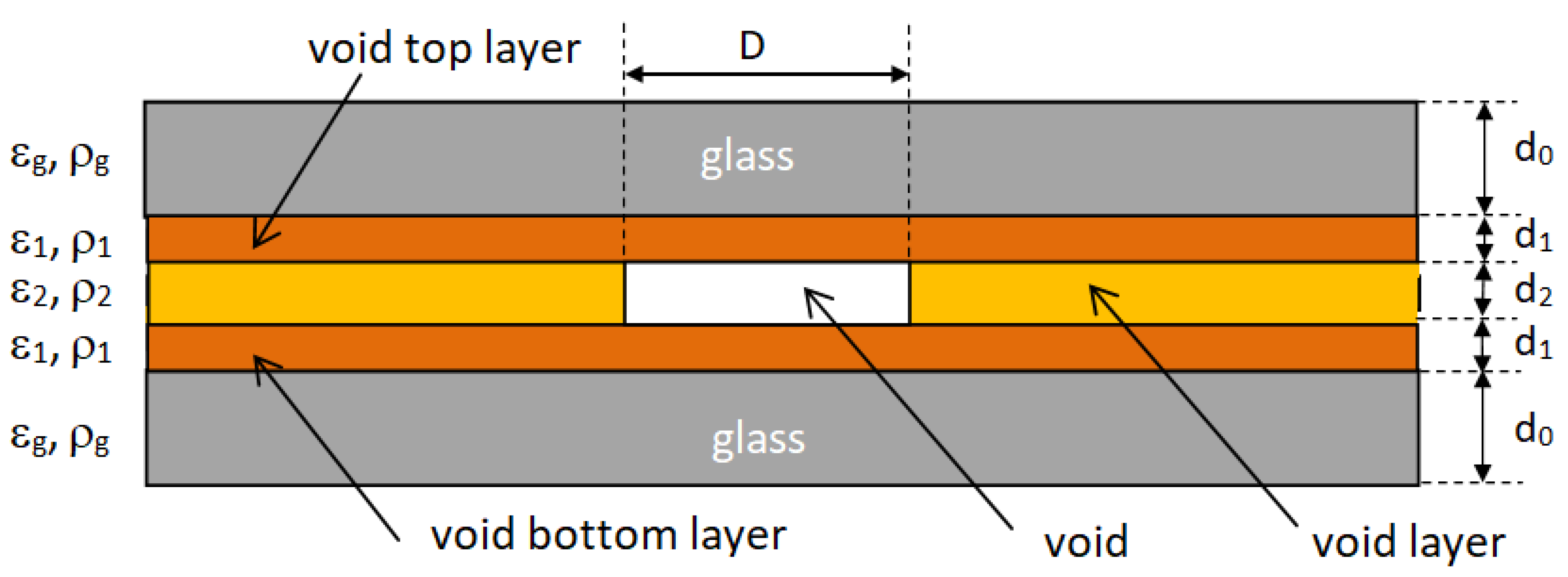
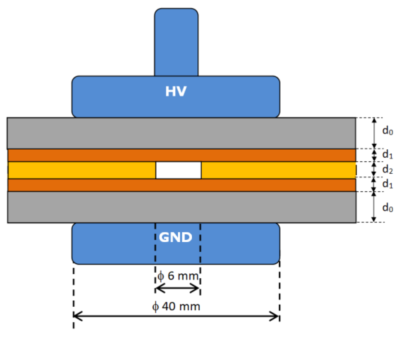
The investigations presented in this paper were performed on the model flat, round cavity (diameter D, thickness d2) embedded in the homogenous insulating material, being a source of discharges. Two glass plates, on upper and bottom side, applied pressure to the void in order to achieve mechanical stability. Such a specimen consists of five layers, i.e., two glass plates with thickness d0 each, layer containing void (thickness d2) and two flakes making the top and bottom side of the cavity with thickness d1 each. The geometrical representation of the specimen is illustrated in Figure 3 and corresponds to the model shown in Figure 1.
Assuming the dielectric relative permittivity ε and resistivity of the dielectric layers ρ:
- ▪
- εg, ρg of the glass plate (layer 0),
- ▪
- ε1, ρ1 of the top/bottom cavity flake (layer 1),
- ▪
- ε2, ρ2 of the layer containing void (layer 2),
and the above mentioned geometry, the approximate partial discharge inception voltage (PDIV) thresholds on the specimen terminals can be estimated, both for AC (Uinc_AC) and DC (Uinc_DC) cases. The equation reflects the AC case taking into account material permittivity and thickness of the insulating layer (assuming relative permittivity of air equal one):
For DC case, material resistivity and layer thickness is considered:
At DC voltage, insulating material conductivity reveals strong temperature dependence, which is not considered in this paper. Hence, the temperature has strong effect at DC voltage on electric field distribution and related charging stage with recovery voltage build-up, including influence on PD dynamics [40]. The measurements presented in this paper were performed at room temperature. The electrode configuration presented in Figure 4 ensures a uniform electric field in a cavity space. Both electrodes have a diameter 40 mm.
The specimen dimensions are summarized in Table 1.
The experiments presented in this paper were performed on insulating paper (PK) and cross-linked polyethylene (XLPE). The electrical properties of the specimens, specifically the permittivity and resistivity, are shown in Table 2.
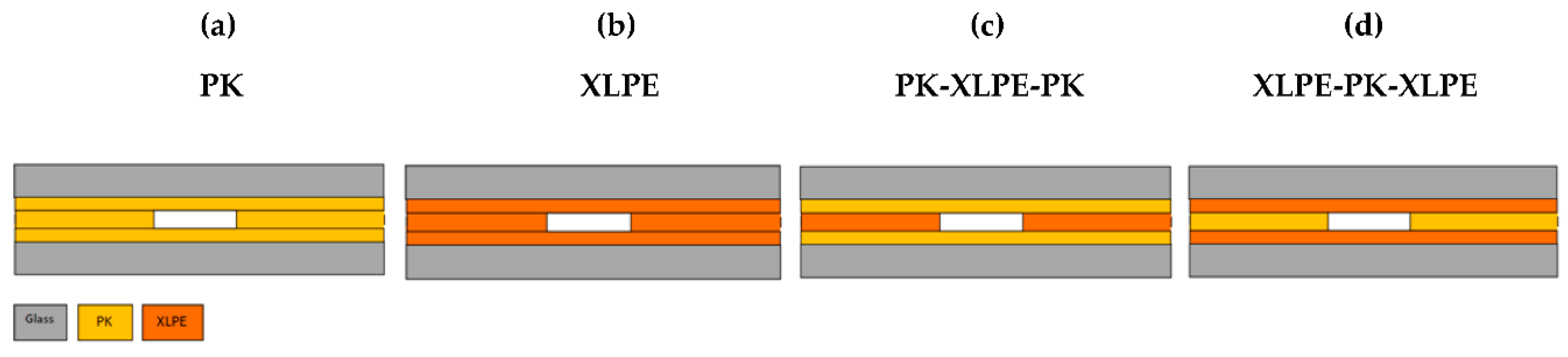
In order to investigate the influence of insulating material resistivity on PD inception and recovery stage, the following four specimens were compared:
- ▪
- PK—(1): specimen made of insulating paper (PK—layer 1 and layer 2),
- ▪
- XLPE—(2): specimen made of polyethylene (XLPE—layer 1 and layer 2),
- ▪
- XLPE-PK-XLPE—(3): void layer 2 made of PK and top/bottom layers 1 made of cross-linked polyethylene (XLPE),
- ▪
- PK-XLPE-PK—(4): void layer 2 made of XLPE and top/bottom layers 1 made of insulating paper (PK).
The geometry of the specimens was kept constant for all above configurations. In all those cases layer 0 refers to glass plate. The graphical representation of specimens is shown in Figure 5.
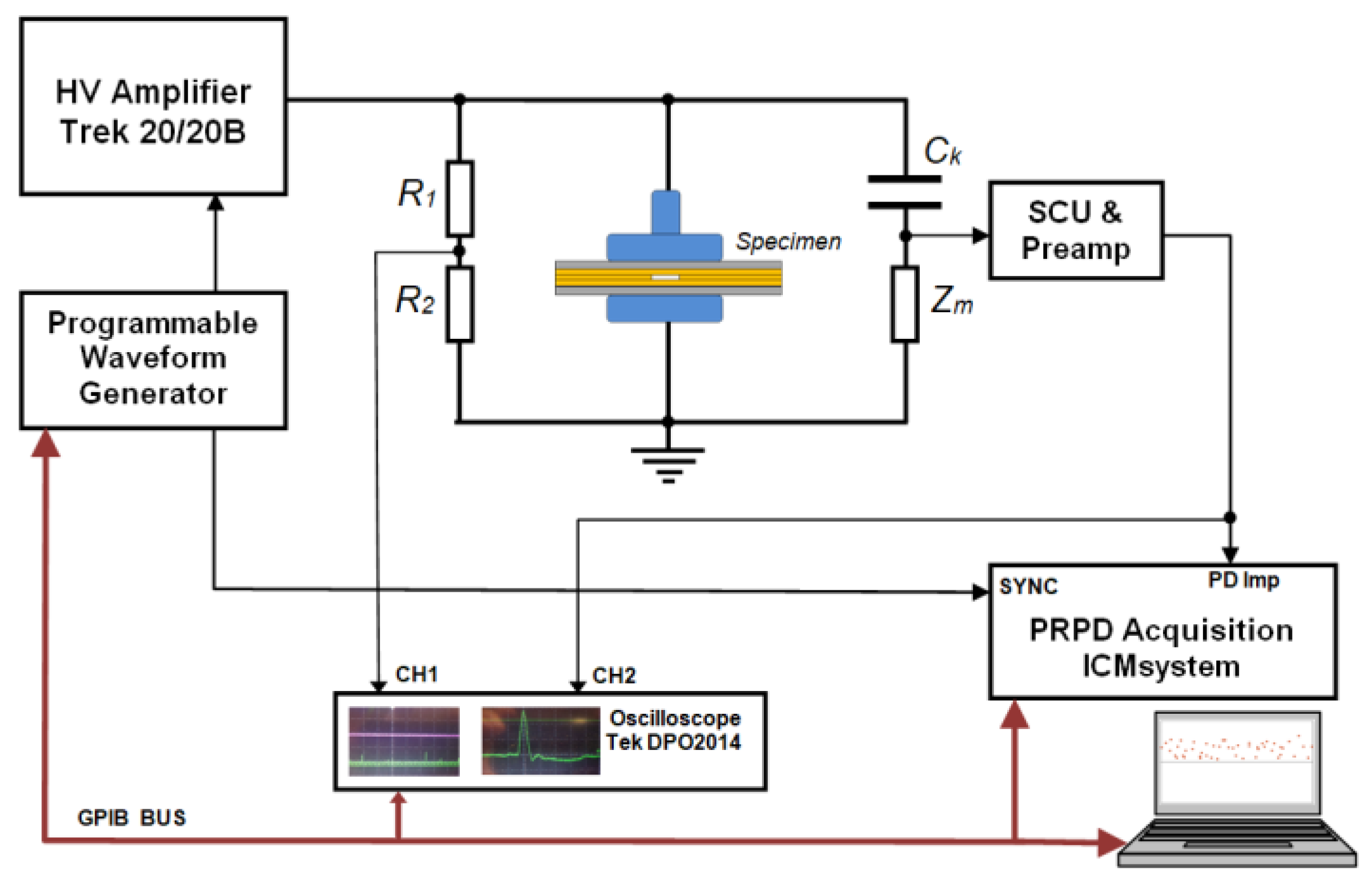
The PD measurements, both at AC and DC voltage, were performed in a setup shown in Figure 6. Partial discharges were recorded using a wideband detection system ICM+, connected to a control unit via GPIB bus. The measurements at DC voltage were carried out in time mode, within defined time interval (up to 600 s in this paper). Both high voltage AC and DC signals were provided by an HV amplifier (TREK 20/20B) controlled by a programmable waveform generator AFG 3102C. The voltage reference signal was obtained from a HV resistive divider (R1, R2). The PD signal was captured using a measuring impedance Zm, connected in series with a coupling capacitor Ck = 100 pF, then filtered and pre-amplified in signal conditioning unit SCU. The AC measurements were recorded within 60 s in a phase-resolved mode resulting in D(φ, q, n) pattern acquisition (8·8·16 bit), whereas in DC mode, the PD pulse distribution in time was obtained. In the latter case, especially the evolution of time interval between pulses was investigated, in a voltage range from inception up to 20 kV DC. In both cases, PDIV was detected.
4. Experimental Results
The experiments have been performed on two types of specimens representing high voltage cable insulation. First one denoted as (PK) represents the insulating paper, while the second one (XLPE) represents the cross linked polyethylene. Both specimens contained the same size of the embedded void shown in Figure 4. For reference, first the partial discharges were measured at AC voltage and then the sequence at DC voltage was recorded. The partial discharge inception voltage thresholds (PDIV) obtained both from calculations (Equations (9) and (10)) and measurements are shown in Table 3. For calculations, the dimensions (Table 1), as well as the electrical permittivity and resistivity (Table 2) were used. The notation PK-XLPE-PK used in this paper means: void layer material XLPE and top/bottom layers PK. The only symbol PK or XLPE denotes the whole specimen made from the homogenous insulating material.
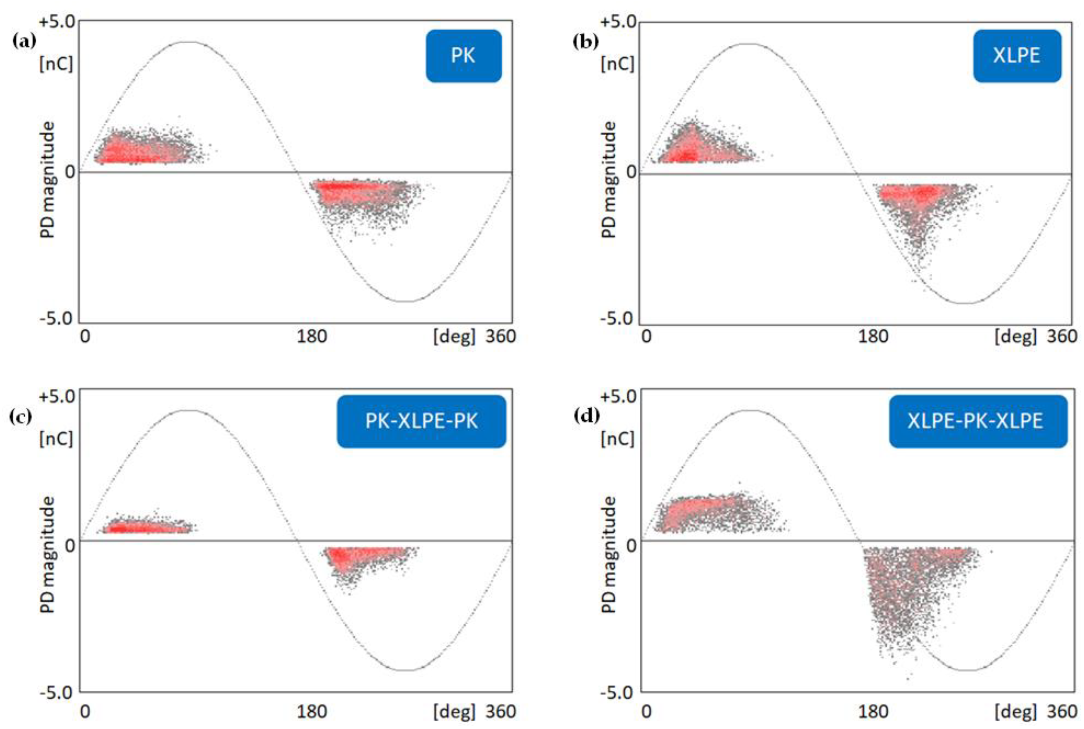
The four specimens having the same geometry but different compositions of insulating materials reveal slightly different PD inception voltages. In AC case, determined mainly by materials permittivity the spread is less visible, than in DC case forced by materials resistivity, where deviations between materials are more pronounced. In AC measurement, the lowest value was detected for PK-XLPE-PK specimen 9.2 kV and the highest one for XLPE-PK-XLPE 9.7 kV. The PDIVAC for PK specimen was 9.5 kV and 9.4 kV for XLPE. Generally, no large scatter between PD inception voltage levels was observed at AC voltage. The PD phase-resolved patterns obtained at PD inception at AC voltage for all specimens are shown in Figure 7. All patterns reveal similar character in terms of phase range, number of discharges and statistical distribution of discharges, since at AC voltage all specimens are very similar.
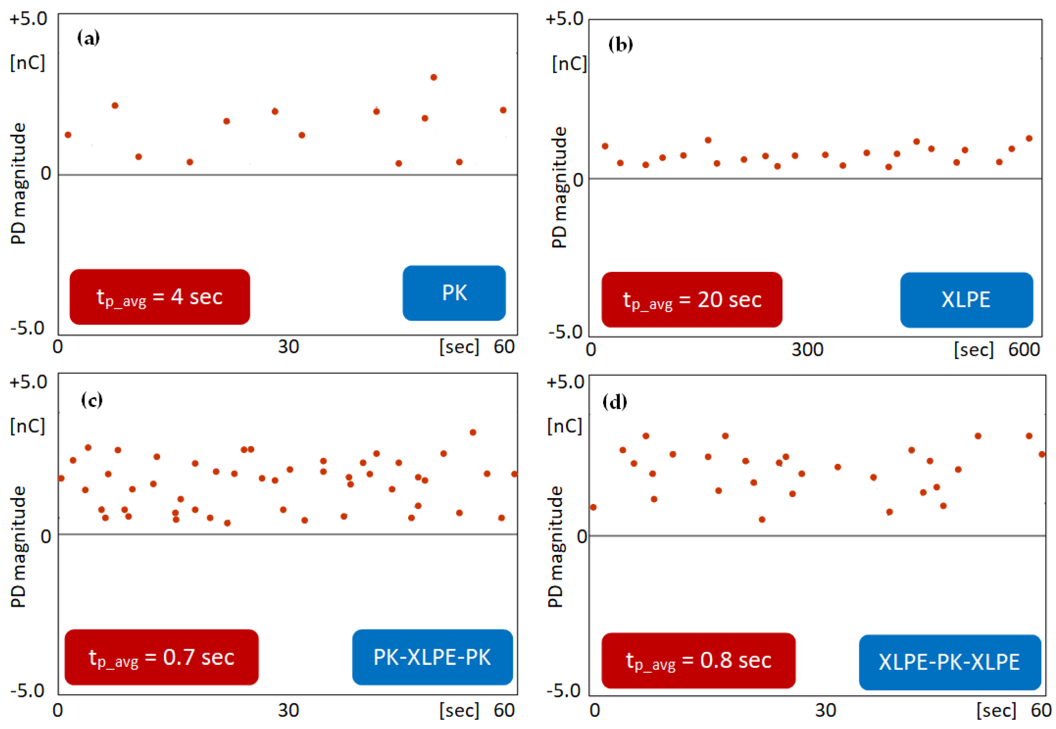
Since there is no reference point in time at DC voltage (unlike voltage zero crossing at AC), the PD patterns show the discharge pulse peak value and a time stamp, in the assumed recording time. Different values of the inter PD pulse time interval result from the impact of the insulation resistivity on recovery voltage time constant τDC. The PD patterns recorded for all specimens at DC voltage 20 kV are shown in Figure 8, with a 60 s zoomed view (600 s for XLPE). Among specimens, the longest average time interval tp_avg equal to 20 s is for (XLPE) (Figure 8b), whereas for (PK) (Figure 8a) it is much shorter—around 4 s, which clearly indicates the effect of the material resistivity. In all cases the void capacitance is the same. In case of DC voltage, the lowest PDIV 9 kV was also calculated for PK-XLPE-PK specimen. In this case the higher resistivity of XLPE with respect to PK leads to higher voltage drop on the void than in reverse case, i.e., lower terminal inception UDC voltage.
It is worth noting the different approach in PDIV determination. In AC case it was assumed stable PD with at least two pulses per period, whereas in DC case the PDIV is much more tricky due to ultra-low repeatability compared to AC case. Thus, in this case it should be interpreted as a detection level. In practice, discharge measurements are usually made with the applied DC voltage equal to several times the inception voltage [41].
5. Discussion
Theoretically, the PD inception voltage at DC voltage should reveal similar values for homogenous specimens with the same geometry. It is to some extent material-independent and mainly influenced by the proportion of the layers’ thickness. However, the PD pulse repetition rate is heavily influenced by material resistivity and capacitance of the void. It was shown that the static PD inception voltage is determined by the resistivity of dielectric material adjacent to the wall void and is not influenced by the gas resistivity, to be usually few orders of magnitude higher. This is of course one of the inception condition apart from the starting electron availability and avalanche multiplication fulfillment.
The apparent capacitance Cc of a gaseous (air filled, ε = 1) cavity (D = 6 mm, d2 = 0.9 mm) equals to:
where ε0 = 8.85·10−12 F·m−1.
The term apparent is used since cavity is not representing a real capacitor [8,9,27]. The calculated resistance of layer number one for both PK and XLPE specimen, based on measured resistivity of both materials, equals to 4.6·1012 Ω and 0.7·1014 Ω, respectively. Hence, the roughly estimated time tp between PD pulses yields 6 s for PK and 80 s for XLPE.
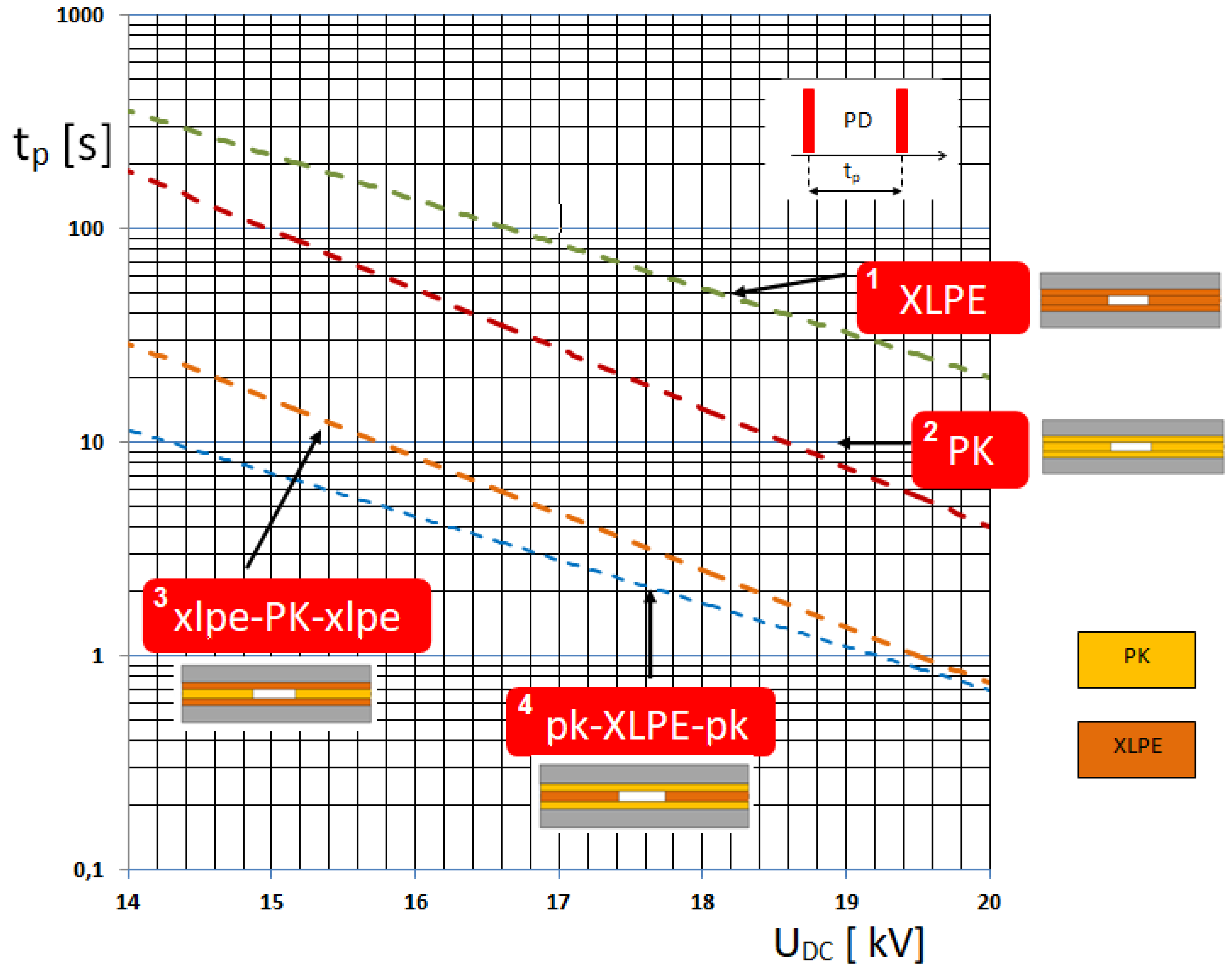
The comparison of the average time tp versus applied voltage in a range from 14 kV to 20 kV for different specimen configurations is shown in Figure 9. In each case, with increasing voltage, the interval between PD pulses decreases. The relationship tp(U) follows an exponential course for all measured configurations.
The measurement results have been shown in semi logarithmic plot and the trend lines approximated by exponential functions, are yielding following relationships between time tp (in seconds) and applied voltage U (in kV):
XLPE tp(U) = 2.8·105 e−0.48U
PK tp(U) = 1·106 e−0.64U
XLPE-PK-XLPE tp(U) = 1.5·105 e−0.61U
PK-XLPE-PK tp(U) = 8·103 e−0.47U
Specimens (1) and (2) represent a homogeneous insulating medium in terms of resistivity, whereas specimens (3) and (4) a heterogeneous one, in which the resistivity can represent different surface conditions of the source of discharges, e.g., degraded due to aging processes. According to the formula (7)—tp(τDC), while increasing material resistivity the time interval will increase. In a heterogeneous dielectric, apart from the effect of resistivity (plots (3) and (4) in Figure 9), one can presume the influence of the surface conditions in the source of discharges on the value of inception and extinction voltages. Non-homogeneous void surfaces can be also related to modeling of aging and erosion processes.
The longest tp time, due to higher material resistivity of XLPE comparing with PK, is observed for homogeneous XLPE specimen. While replacing in this specimen the cavity layer by PK material, the curve has moved down, reflecting the influence of the cavity wall material indicated in a model in Figure 2c. The lower surface resistivity of PK with respect to XLPE results in bypassing the void capacitance during charging period and recovery voltage build-up. Considering PK specimen, the replacement of the middle void layer by XLPE results in slightly lower DC inception voltage, i.e., 11.5 kV for PK vs. 9.0 kV for PK-XLPE-PK, thus higher repetition of PD pulse in the latter case.
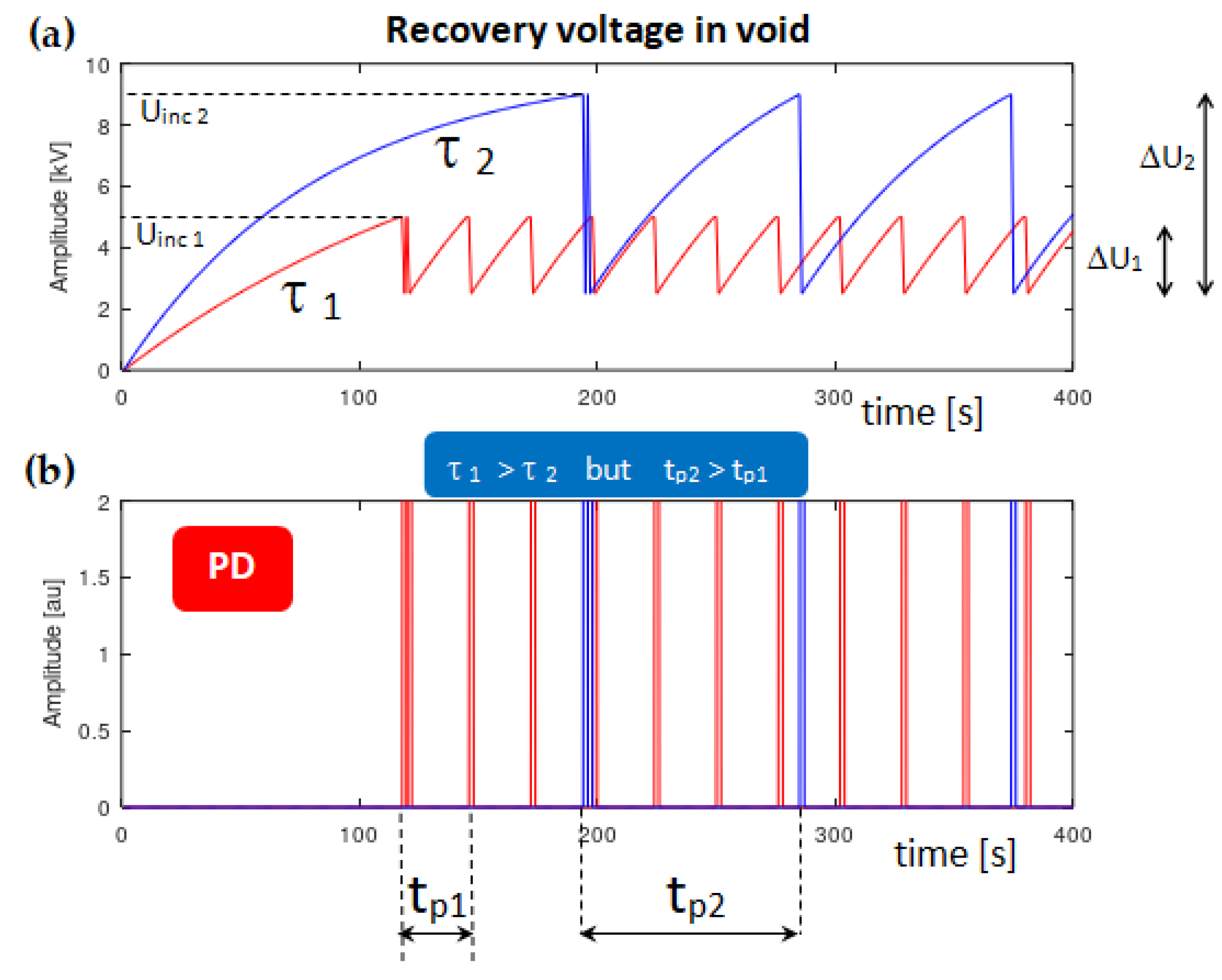
As was mentioned before, for small cavities the PD inception voltage threshold strongly depends on cavity thickness. The simulation presented in Figure 10 is highlighting this effect for two cavities: (1) with thickness 1.3 mm (red line) and (2) with thickness 2.3 mm (blue line). Since the void capacitance in the second case is half of the thinner one (Cc1 = 2Cc2), the corresponding time constants have relationship τ1 > τ2. However, taking into account the effect of thickness dependent electric field strength, the breakdown electric field in the first case will be 4.2 kV/mm which corresponds to the inception voltage Uinc1 = 5.5 kV, whereas in the second case for electric field 3.7 kV/mm the inception voltage is Uinc2 = 8.6 kV. This interplay impacts the occurrence of PD pulses (Figure 10b) and as visualized in Figure 10a for τ1 > τ2, results in tp2 > tp1.
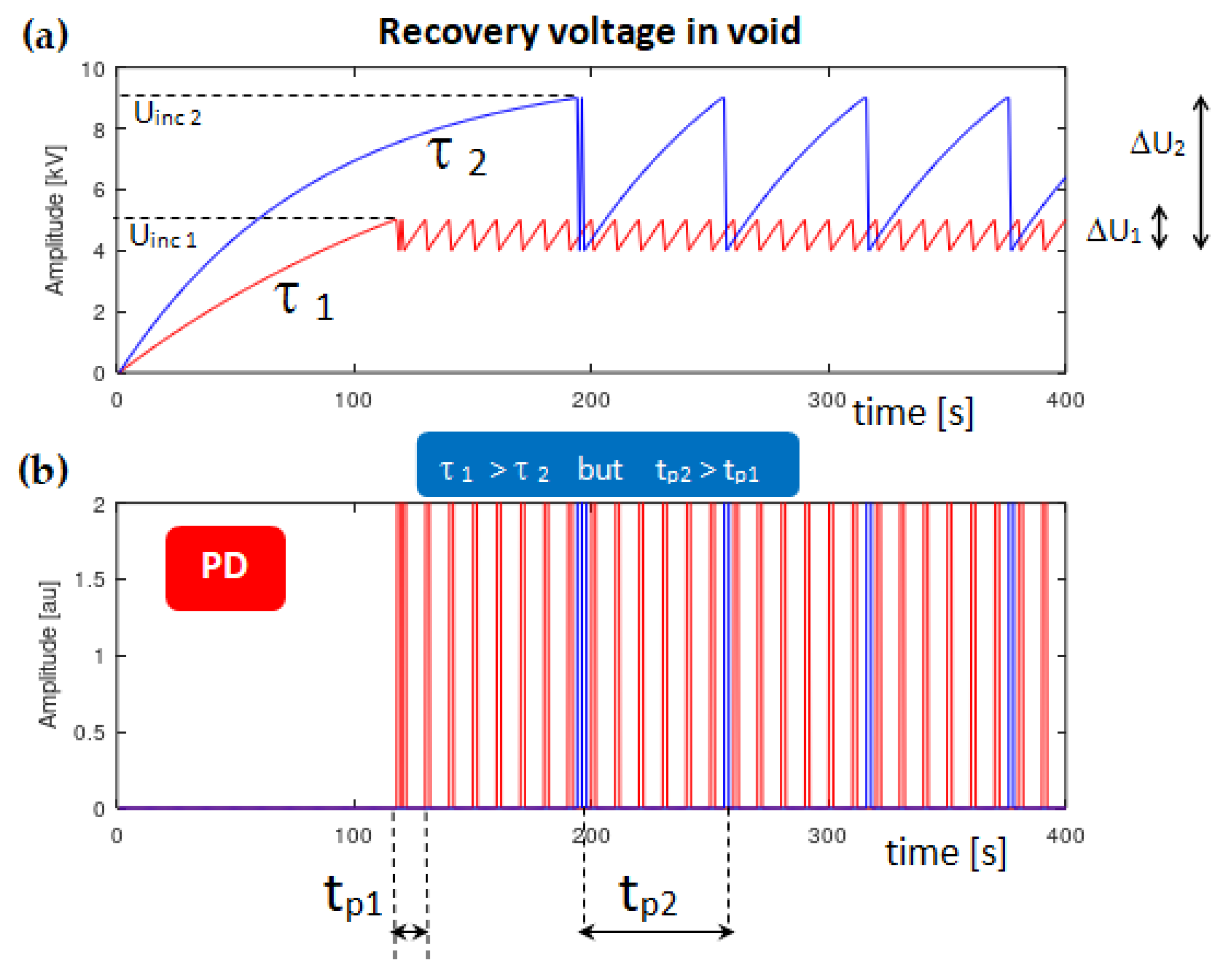
The effect is even more predominant rising the PD extinction voltage from 2.5 kV (Figure 10a) to 4 kV in Figure 11. The void surface conductivity strongly depends in polymeric materials on the PD dynamics, hence surface erosion, aging is leading to greater material surface conductivity, thus lower PD extension voltage.
The voltage drop ΔU on void capacitance Cc due to partial discharge equals to:
The extinction voltage represents the charge Q neutralization conditions in the discharge source:
Extinction voltage Uext can assume certain value (Uext ≠ 0) depending on the surface discharging dynamics in the discharge source. Depending on the extinction voltage level, the void charging voltage can assume waveforms shown in Figure 10 and Figure 11. Additionally, in case of the train of PD pulses the memory effect of charges accumulated on the void surface [34,36] should be considered, due to an alternating effect of the resultant electric field distribution inside the void. Not neutralized surface charges also influence time lag, throughout starting electron availability. Since this paper is focused on highlighting the influence of dielectric material properties on PD modeling and basic processes, those effects were not considered.
The time interval tp between consecutive PD pulses depends on:
- ▪
- volume resistivity ρ of the solid dielectric, and the higher the resistivity value, the longer the time interval,
- ▪
- thickness of the solid dielectric,
- ▪
- capacitance Cc representing the gaseous inclusion, including its thickness and surface. The void thickness has influence on the PD inception voltage. While increasing cavity thickness within certain range, the inception voltage Uinc will decrease, resulting in the reduction of the time interval tp.
- ▪
- extinction voltage Uext.
The last factor, which is the extinction voltage Uext, is directly related to the state of the surface between which the discharge develops (walls of a cavity). This state determines, in the most general terms, the value of its surface resistivity, which in gas inclusion has an impact on the accumulation of charges on its surface. The degree of discharge concentration on this surface before subsequent discharges may vary. Incomplete neutralization of gas inclusion surface means that there is residual potential after the discharge event, denoted as extinction voltage. The random nature of both inception voltage Uinc and extinction voltage Uext leads to statistical analysis of the set of impulses of discharges, and thus the time intervals tp between recorded impulses. Assuming the probability distribution (e.g., normal distribution) of the Uinc and Uext voltage values, the partial discharge mechanism at DC voltage can be illustrated by a combination of time intervals tp and applied high voltage values. The above analysis of the impact of various factors on the value of the time interval tp between pulses refers to the elements in the equivalent circuit of the insulation system with the source of discharges in the form of gas-filled inclusion. An additional factor of fluctuations, mentioned above, in the theoretical model of discharges may be the “field effect”, as a result of the accumulation of discharge charges on boundary surfaces in the sources of discharges and interaction with charges in the solid dielectric. This effect applies in particular to dielectrics with polar structures from the group of synthetic polymers.
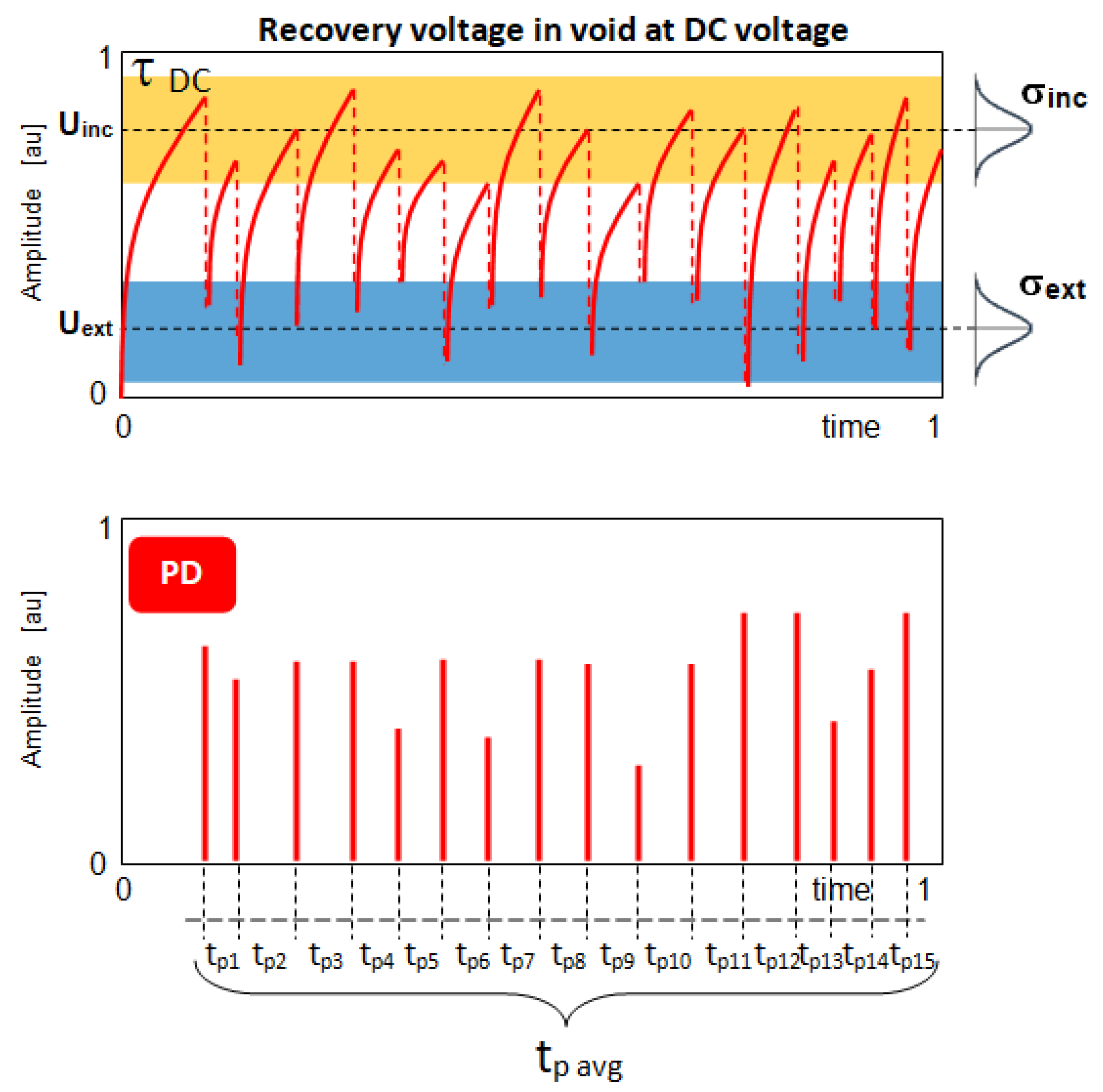
In a stationary model, the time interval tp is constant. The average tp time obtained from measurements results from the stochastically modified inter-PD pulse intervals. In the exemplary case presented below, the implemented variability of inception and extinction threshold levels is based on normal Gaussian distribution with assumed standard deviations σinc and σext. The graphical illustration of a stochastic PD model at DC voltage is shown in Figure 12.
The analysis of the mechanism of partial discharges in insulation systems at DC voltage leads to the determination of the quantity that can be used as an indicator of the state of insulation due to the destructive processes occurring in it under the action of partial discharges. In this analysis based on discharge modeling, the term “insulation state” refers to the surface transformation processes in gas inclusion, known as erosion processes. The occurrence of these processes can be evaluated in long-term laboratory aging tests. The diagnostic indicator of the insulation system condition due to the effect of partial discharges in it may be the number of pulses in the detection circuit in the predefined time period, resulting from the time interval between successive pulses.
6. Conclusions
This paper reports the influence of insulating material properties on partial discharges at DC voltage. The investigations were performed on two kinds of dielectric material used in power cables. Various combinations of specimens were designed to reveal the effect of the material resistivity on the PD activity. The modified PD model was applied to analyze both inception and post discharge recovery stage. The role of dielectric properties of material adjacent to the void was investigated, highlighting its impact during static inception stage and in charging stage. In the latter one, both volume resistivity and surface resistivity of cavity walls are involved. The void adjacent material properties play a key role setting the inception voltage threshold at DC voltage. The interplay between the gaseous void resistivity and the solid dielectric resistivity was highlighted, which is especially important for proper modeling and simulations of partial discharges at DC voltage.
Despite many simplifications introduced in the model, measurement results have confirmed the role of the dielectric material surrounding the void on partial discharge dynamics. The average time interval between PD pulses revealed systematic relationship with respect to the applied voltage and specimen properties. Variability of this time signature in a stochastic PD model at DC voltage was shown with respect to the stochastic changes of both partial discharge inception and extinction voltage levels according to normal distribution. The longest average time between consecutive PD pulses, due to higher material resistivity of XLPE comparing with PK, is observed for homogeneous XLPE specimen. This value can be considered in the future research for diagnostic indicator at DC voltage.
Funding
This research received no external funding.
Conflicts of Interest
The author declares no conflict of interest.
References
- Jacob, N.D.; McDermid, W.M.; Kordi, B. On-line monitoring of partial discharges in a HVDC station environment. IEEE Trans. Dielectr. Electr. Insul. 2012, 19, 925–935. [Google Scholar] [CrossRef]
- Fard, M.A.; Farrag, M.E.; Reid, A.J.; Al-Naemi, F. Electrical Treeing in Power Cable Insulation under Harmonics Superimposed on Unfiltered HVDC Voltages. Energies 2019, 12, 3113. [Google Scholar] [CrossRef] [Green Version]
- Shekhar, A.; Feng, X.; Gattozzi, A.L.; Hebner, R.E.; Wardell, D.; Strank, S.; Mor, A.R.; Ramirez-Elizondo, L.M.; Bauer, P. Impact of DC Voltage Enhancement on Partial Discharges in Medium Voltage Cables—An Empirical Study with Defects at Semicon-Dielectric Interface. Energies 2017, 10, 1968. [Google Scholar] [CrossRef] [Green Version]
- Götz, T.; Kirchner, H.; Backhaus, K. Partial Discharge Behaviour of a Protrusion in Gas-Insulated Systems under DC Voltage Stress. Energies 2020, 13, 3102. [Google Scholar] [CrossRef]
- Gemant, A.; Philippoff, W. Die Funkenstrecke mit Vorkondensator. Zeitschrift Technol. Physik 1932, 9, 425–430. [Google Scholar]
- Kreuger, F.H. Discharge Detection in High Voltage Equipment; Temple Press: London, UK, 1964; 237p. [Google Scholar]
- Partial Discharge Measurements; IEC Publication 60270-2000; IEC: Geneva, Switzerland, 2000; Available online: https://webstore.iec.ch/publication/1247 (accessed on 15 July 2020).
- Hauschild, W.; Lemke, E. High-Voltage Test and Measuring Techniques; Springer: Berlin/Heidelberg, Germany, 2014; ISBN 978-3-642-45351-9. [Google Scholar]
- Pedersen, A. On the electrodynamics of partial discharges in voids in solid dielectrics. In Proceedings of the 3rd International Conference on Conduction and Breakdown in Solid Dielectrics, Trondheim, Norway, 1 January 1989. [Google Scholar]
- Lemke, E. A critical review of partial-discharge models. IEEE Electr. Insul. Mag. 2012, 28, 11–16. [Google Scholar] [CrossRef]
- Achillides, Z.; Kyriakides, E.; Danikas, M.G. Partial discharge modeling: An advanced capacitive model of void. IEEE Trans. Dielectr. Electr. Insul. 2019, 26, 1805–1813. [Google Scholar] [CrossRef]
- Achillides, Z.; Danikas, M.G.; Kyriakides, E. Partial discharge modeling and induced charge concept: Comments and criticism of pedersen’s model and associated measured transients. IEEE Trans. Dielectr. Electr. Insul. 2017, 24, 1118–1122. [Google Scholar] [CrossRef]
- Kreuger, F.H.; Fromm, U. Partial Discharges in Gaseous Voids for DC Voltage. JPN J. Appl. Phys. 1994, 33, 1079–1084. [Google Scholar] [CrossRef]
- Rodríguez-Serna, J.; Albarracín-Sánchez, R.; Dong, M.; Ren, M. Computer Simulation of Partial Discharges in Voids inside Epoxy Resins Using Three-Capacitance and Analytical Models. Polymers 2020, 12, 77. [Google Scholar] [CrossRef] [Green Version]
- Mahdipour, M.; Akbari, A.; Werle, P. Charge concept in partial discharge in power cables. IEEE Trans. Dielect. Electr. Insul. 2017, 24, 817–825. [Google Scholar] [CrossRef]
- Niemeyer, L.; Fruth, B.; Gutfleisch, F. Simulation of Partial Discharges in Insulation Systems. In 7th International Symposium on High Voltage Engineering; ISH: Dresden, Germany, 1991. [Google Scholar]
- Niemeyer, L. A generalized approach to partial discharge modeling. IEEE Trans. Dielectr. Electr. Insul. 1995, 2, 510–528. [Google Scholar] [CrossRef] [Green Version]
- Forssen, C.; Edin, H. Partial discharges in a cavity at variable applied frequency part 2: Measurements and modeling. IEEE Trans. Dielectr. Electr. Insul. 2008, 15, 1610–1616. [Google Scholar] [CrossRef]
- Illias, H.; Chen, G.; Lewin, P.L. Partial discharge behavior within a spherical cavity in a solid dielectric material as a function of frequency and amplitude of the applied voltage. IEEE Trans. Dielectr. Electr. Insul. 2011, 18, 432–443. [Google Scholar] [CrossRef]
- Illias, H.; Chen, G.; Lewin, P.L. Comparison between three-capacitance, analytical-based and finite element analysis partial discharge models in condition monitoring. IEEE Trans. Dielectr. Electr. Insul. 2017, 24, 99–109. [Google Scholar] [CrossRef]
- Serdyuk, Y.; Gubanski, S. Computer modeling of interaction of gas discharge plasma with solid dielectric barriers. IEEE Trans. Dielectr. Electr. Insul. 2005, 12, 725–735. [Google Scholar] [CrossRef]
- Georghiou, G.E.; Papadakis, A.P.; Morrow, R.; Metaxas, A.C. Numerical modelling of atmospheric pressure gas discharges leading to plasma production. J. Phys. D Appl. Phys. 2005, 38, R303–R328. [Google Scholar] [CrossRef]
- Pan, C.; Meng, Y.; Wu, K.; Han, Z.; Qin, K.; Cheng, Y. Simulation of partial discharge sequences using fluid equations. J. Phys. D Appl. Phys. 2011, 44, 255201. [Google Scholar] [CrossRef]
- Pan, C.; Song, W.; Tang, J.; Luo, Y.; Luo, X. The Influence of Sample Configuration on PD Frequency at DC Voltage. In Proceedings of the 2018 IEEE International Conference on High Voltage Engineering and Application (ICHVE), Athens, Greece, 1–31 December 2018. [Google Scholar]
- Pan, C.; Tang, J.; Song, W.; Luo, Y.; Wang, D.; Zhuo, R.; Fu, M. Investigation of cavity PD physical processes at DC voltage by simulation. IEEJ Trans. Electr. Electron. Eng. 2018, 13, 1376–1383. [Google Scholar] [CrossRef]
- Callender, G. Modelling Partial Discharge in Gaseous Voids. Ph.D. Thesis, University of Southampton, Southampton, UK, 2018. [Google Scholar]
- Pan, C.; Chen, G.; Tang, J.; Wu, K. Numerical modeling of partial discharges in a solid dielectric-bounded cavity: A review. IEEE Trans. Dielectr. Electr. Insul. 2019, 26, 981–1000. [Google Scholar] [CrossRef] [Green Version]
- Devins, J.C. The 1984 J. B. Whitehead Memorial Lecture the Physics of Partial Discharges in Solid Dielectrics. IEEE Trans. Dielectr. Electr. Insul. 1984, 19, 475–495. [Google Scholar] [CrossRef]
- Densley, R.J. Partial Discharges under Direct Voltage Conditions; Bartnikas, R., Ed.; Engineering Dielectrics; ASTM: Baltimore, MD, USA, 1979. [Google Scholar]
- Fromm, U. Partial Discharge and Breakdown Testing at DC Voltage. Ph.D. Thesis, Delft University, Delft, The Netherlands, 1995. [Google Scholar]
- Seri, P.; Cirioni, L.; Naderiallaf, H.; Montanari, G.C.; Hebner, R.; Gattozzi, A.; Feng, X. Partial Discharge Inception Voltage in DC insulation systems: A comparison with AC voltage supply. In Proceedings of the IEEE Electrical Insulation Conference (EIC), Calgary, AB, Canada, 16–19 June 2019. [Google Scholar]
- Florkowski, M.; Krześniak, D.; Kuniewski, M.; Zydroń, P. Partial Discharge Imaging Correlated with Phase-Resolved Patterns in Non-Uniform Electric Fields with Various Dielectric Barrier Materials. Energies 2020, 13, 2676. [Google Scholar] [CrossRef]
- Krinberg, I.A. Electrical conductivity of air in the presence of an impurity. J. Appl. Mech. Tech. Phys. 1966, 6, 66–71. [Google Scholar] [CrossRef]
- Pan, C.; Wu, K.; Chen, G.; Gao, Y.; Florkowski, M.; Lv, Z.; Ju, T. Understanding Partial Discharge Behavior from the Memory Effect Induced by Residual Charges: A Review. IEEE Trans. Electr. Insul. 2020, 27. Available online: https://www.researchgate.net/publication/342352689 (accessed on 15 July 2020). [CrossRef]
- Bartnikas, R. Some observations concerning the influence of dielectric surfaces upon the PD behavior. IEEE Trans. Dielectr. Electr. Insul. 2008, 15, 1488–1493. [Google Scholar] [CrossRef]
- Florkowski, M.; Florkowska, B.; Zydron, P. Partial discharge echo obtained by chopped sequence. IEEE Trans. Dielectr. Electr. Insul. 2016, 23, 1294–1302. [Google Scholar] [CrossRef]
- Florkowski, M.; Florkowska, B.; Kuniewski, M.; Zydron, P. Mapping of discharge channels in void creating effective partial discharge area. IEEE Trans. Dielectr. Electr. Insul. 2018, 25, 2220–2228. [Google Scholar] [CrossRef]
- Akram, S.; Wang, P.; Nazir, M.T.; Zhou, K.; Bhutta, M.S.; Hussain, H. Impact of impulse voltage frequency on the partial discharge characteristic of electric vehicles motor insulation. Eng. Fail. Anal. 2020, 116, 104767. [Google Scholar] [CrossRef]
- Florkowska, B. Electrical Strength of High Voltage Gas Insulated Systems; AGH Press: Kraków, Poland, 2003; ISBN 83-89388-01-4. (In Polish) [Google Scholar]
- Gu, X.; Xu, Y.; Yan, Y.; Zhao, P. Partial discharge in a cylindrical cavity in XLPE under DC voltage: Simulation and experiment. IEEE Trans. Dielectr. Electr. Insul. 2019, 26, 1831–1839. [Google Scholar] [CrossRef]
- Melville, D.; Salvage, B.; Steinberg, N. Discharge detection and measurement under direct-voltage conditions: Significance of discharge magnitude. Proc. Inst. Electr. Eng. 1965, 112, 1815. [Google Scholar] [CrossRef]
Figure 1.
Equivalent circuit for partial discharge (PD) modeling at direct current (DC).

Figure 2.
(a) PD model at DC reflecting the role of material resistivity adjacent to the void, (b) equivalent circuit of inception stage, RA—resistance adjacent to the void (combination of components Ra2, R’a2), R0—resultant resistance from combination of components Ra1, R’a1, Ra3, R’a3, Rb, R’b, (c) equivalent circuit of charging stage, UDC—terminal voltage on a specimen.

Figure 3.
Dielectric layered specimen and notation, ε—dielectric relative permittivity, ρ—electric resistivity, d—thickness, D—void diameter (explanation in text).
Figure 3.
Dielectric layered specimen and notation, ε—dielectric relative permittivity, ρ—electric resistivity, d—thickness, D—void diameter (explanation in text).

Figure 4.
Specimen with electrodes.

Figure 5.
Graphical representation of specimen configurations: (a) insulating paper (PK), (b) polyethylene (XPLE), (c) top/bottom insulating paper, void layer XLPE, (d) top/bottom XLPE, void layer PK.
Figure 5.
Graphical representation of specimen configurations: (a) insulating paper (PK), (b) polyethylene (XPLE), (c) top/bottom insulating paper, void layer XLPE, (d) top/bottom XLPE, void layer PK.

Figure 6.
Measuring set-up for PD acquisition at AC and DC voltage: R1, R2—resistive divider, Ck—coupling capacitor, Zm—coupling impedance, SCU—signal conditioning unit and preamplifier.
Figure 6.
Measuring set-up for PD acquisition at AC and DC voltage: R1, R2—resistive divider, Ck—coupling capacitor, Zm—coupling impedance, SCU—signal conditioning unit and preamplifier.

Figure 7.
Partial discharges patterns at AC inception voltage for specimens: (a) PK, (b) XLPE, (c) PK-XLPE-PK, (d) XLPE-PK-XLPE.
Figure 7.
Partial discharges patterns at AC inception voltage for specimens: (a) PK, (b) XLPE, (c) PK-XLPE-PK, (d) XLPE-PK-XLPE.

Figure 8.
Partial discharges patterns at 20 kV DC voltage for specimens: (a) PK, (b) XLPE, (c) PK-XLPE-PK, (d) XLPE-PK-XLPE.
Figure 8.
Partial discharges patterns at 20 kV DC voltage for specimens: (a) PK, (b) XLPE, (c) PK-XLPE-PK, (d) XLPE-PK-XLPE.

Figure 9.
The relationship of time tp between consecutive PD pulses versus applied DC voltage UDC for various specimen configurations.
Figure 9.
The relationship of time tp between consecutive PD pulses versus applied DC voltage UDC for various specimen configurations.

Figure 10.
Influence of cavity thickness (1.3 mm—red, 2.3 mm—blue) on recovery voltage build up and time tp between consecutive PD pulses, (a) cavity charging voltage, (b) PD pulses (Uext = 2.5 kV).
Figure 10.
Influence of cavity thickness (1.3 mm—red, 2.3 mm—blue) on recovery voltage build up and time tp between consecutive PD pulses, (a) cavity charging voltage, (b) PD pulses (Uext = 2.5 kV).

Figure 11.
Influence of cavity thickness (1.3 mm—red, 2.3 mm—blue) on recovery voltage build up and time tp between consecutive PD pulses, (a) cavity charging voltage, (b) PD pulses (Uext = 4 kV).
Figure 11.
Influence of cavity thickness (1.3 mm—red, 2.3 mm—blue) on recovery voltage build up and time tp between consecutive PD pulses, (a) cavity charging voltage, (b) PD pulses (Uext = 4 kV).

Figure 12.
Variability of tp time in a stochastic PD model at DC voltage, variable inception Uci and extinction Uce voltage levels according to normal distribution with standard deviation σinc and σext, respectively.
Figure 12.
Variability of tp time in a stochastic PD model at DC voltage, variable inception Uci and extinction Uce voltage levels according to normal distribution with standard deviation σinc and σext, respectively.


Table 1.
Specimen dimensions.
| D | d0 | d1 | d2 | |
|---|---|---|---|---|
| Dimension [mm] | 6 | 2 | 0.5 | 0.9 |
Table 2.
Electrical properties of materials in specimens.
| Glass | PK | XLPE | |
|---|---|---|---|
| Surface resistivity [Ω] | 8.0·1010 | 2.0·1012 | 2·1013 |
| Volume resistivity [Ω·m] | 1.1·1011 | 4.6·1013 | 6·1014 |
| Relative dielectric permittivity | 7.9 | 2.8 | 2.4 |
Table 3.
Partial discharge terminal inception voltage calculated and measured at AC and DC voltage.
| PDIV AC [kV] | ||||
|---|---|---|---|---|
| PK | XLPE | PK-XLPE-PK | XLPE-PK-XLPE | |
| calculated | 9.3 | 9.1 | 8.8 | 9.1 |
| detected | 9.5 | 9.4 | 9.2 | 9.7 |
| PDIV DC [kV] | ||||
| calculated | 11.5 | 10.5 | 9.0 | 11.0 |
| detected | 14.0 | 12.0 | 13.0 | 12.0 |
© 2020 by the author. Licensee MDPI, Basel, Switzerland. This article is an open access article distributed under the terms and conditions of the Creative Commons Attribution (CC BY) license (http://creativecommons.org/licenses/by/4.0/).
Share and Cite
MDPI and ACS Style
Florkowski, M. Influence of Insulating Material Properties on Partial Discharges at DC Voltage. Energies 2020, 13, 4305. https://doi.org/10.3390/en13174305
AMA Style
Florkowski M. Influence of Insulating Material Properties on Partial Discharges at DC Voltage. Energies. 2020; 13(17):4305. https://doi.org/10.3390/en13174305
Chicago/Turabian StyleFlorkowski, Marek. 2020. "Influence of Insulating Material Properties on Partial Discharges at DC Voltage" Energies 13, no. 17: 4305. https://doi.org/10.3390/en13174305
Note that from the first issue of 2016, this journal uses article numbers instead of page numbers. See further details here.