A High-Efficiency Isolated LCLC Multi-Resonant Three-Port Bidirectional DC-DC Converter


School of Electrical and Information Engineering, Tianjin University, Tianjin 300072, China
*
Author to whom correspondence should be addressed.
†
These authors contributed equally to this work.
Energies 2017, 10(7), 934; https://doi.org/10.3390/en10070934
Submission received: 13 May 2017
/
Revised: 25 June 2017
/
Accepted: 3 July 2017
/
Published: 5 July 2017
Abstract
:In this paper, an isolated multi-resonant three-port bidirectional direct current-direct current (DC-DC) converter is proposed, which is composed of three full bridges, two inductor-capacitor-inductor-capacitor (LCLC) multi-resonant tanks and a three-winding transformer. The phase shift control method is employed to manage the power transmission among three ports. Relying on the appropriate parameter selection, both of the fundamental and the third order power can be delivered through the multi-element LCLC resonant tanks, and consequently, it contributes to restrained circulating energy and the desirable promoted efficiency. Besides, by adjusting the driving frequency under different load conditions, zero-voltage-switching (ZVS) characteristics of all the switches of three ports are guaranteed. Therefore, lower switching loss and higher efficiency are achieved in full load range. In order to verify the feasibility of the proposed topology, a 1.5 kW prototype is established, of which the maximum efficiencies under forward and reverse operating conditions are 96.7% and 96.9% respectively. In addition, both of the bidirectional efficiencies maintain higher than 95.5% when the power level is above 0.5 kW.
1. Introduction
Nowadays, facing the increasingly severe energy crisis and pollution issues, considerable attention is being focused on renewable power sources to figure out promising solutions [1,2,3]. However, owing to the time-varying and intermittent output features of some renewable sources, energy storage plays an indispensable role to improve the stability and energy utilization rate of the distributed energy generation system (DEGS) [4,5,6]. In existing DEGS, the renewable energy sources, storage units and loads are connected together by their independent converters. Therefore, the large number of converters leads to complexity in the DEGS architecture. This issue is addressed by adopting three-port converters, where the efficiency, the cost and the power density are optimized. As a consequence, three-port bidirectional DC-DC converters (TP-BDCs) have become a competitive alternative in recent years.
Based on the connections, the TP-BDCs are simply categorized into three types, namely the non-isolated, the partly-isolated and the isolated converters [7]. For the non-isolated topology, although the direct connection is beneficial for its reduced number of components and compact architecture, this kind of TP-BDC suffers from limited voltage gain, since the voltage conversion ratio can only be adjusted by controlling the duty-ratio of switches [8,9,10]. In the partly-isolated structures, a transformer is used to isolate one port from the other two ports. Owing to the added transformer, is easier to obtain higher voltage gain with the partly-isolated TP-BDC [11,12,13,14]. However, neither non-isolated or partly-isolated TP-BDCs are suitable for applications where the three ports must be completely isolated. Therefore, it is necessary to consider the isolated-type TP-BDC [15,16].
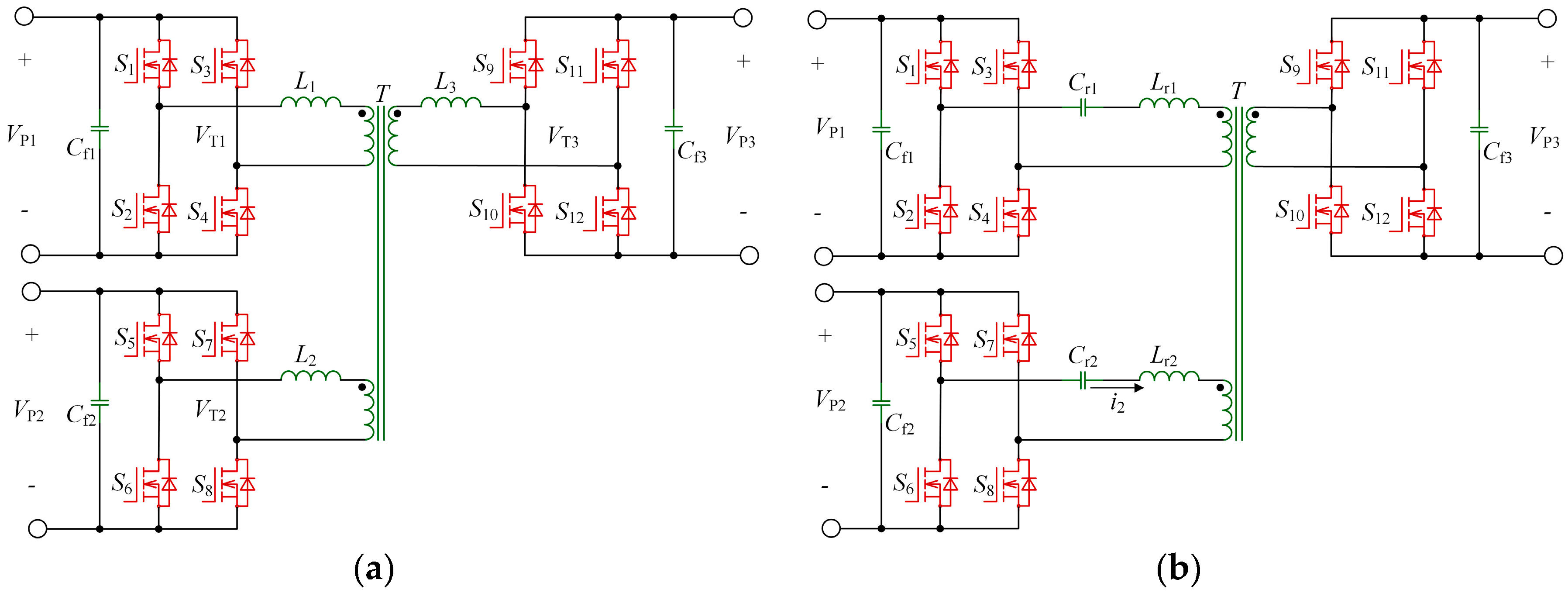
The isolated TP-BDC exhibits pronounced advantages over its two counterparts, since the three-port power exchanges are realized through a three-winding high-frequency transformer, and the completely galvanic isolation is also ensured. Furtherly, among the numerous previously published references [17,18,19,20,21,22,23,24] about isolated TP-BDCs, two more detailed main sub-classifications are used: the triple-active-bridge (TAB) converter shown in Figure 1a and the series-resonant TP-BDC (SR-TP-BDC) in Figure 1b.
The TAB converter, a research hotspot, is composed of three active bridges, three inductors and a three-winding transformer [17,18,19,20,21]. It possesses advantages such as galvanic isolation, bidirectional power flow, ZVS operation and phase shift control with fixed switching frequency, while the power coupling among the three ports makes the decoupling matrix essential in its control loop, which is sophisticated and can be detrimental to the reliability of TAB. Moreover, the power transmission in TAB topology is in inverse proportion of the impedance of L1–L3, and L1–L3 are inherent greater than the leakage inductors of transformer. Consequently, the switching frequency has to be reduced in case of high power levels. In [19,20,21] the driving frequencies are all 20 kHz, and this will be detrimental for the desired high power density.
The other sub-classification is the series-resonant TP-BDC (SR-TP-BDC) as Figure 1b shows. Compared to TAB, the SR-TP-BDC introduces two additional series-resonant tanks into the primary sides. For one thing, it maintains the main advantages of TAB such as galvanic isolation, bidirectional operation, ZVS features and constant switching frequency [22,23,24]. For another, the decoupling of the power transmissions successfully relieves the difficulty of control issue. Additionally, another benefit of SR-TP-BDC is that the impedance of SR tanks can be regulated by Cr1, Lr1, Cr2, Lr2 and the driving frequency together, thus, it can operate with a higher switching frequency with realizable component values under high power level. In [23,24], renewable source, battery and load are integrated to a three-port SR BDC. The driving frequency rises to 100 kHz, which is apparently higher than 20 kHz of TAB [19,20,21].
In spite of the benefits discussed above, the SR-TP-BDC still needs to be modified due to the loss of ZVS at light load. Since the phase shift angle is small under light load conditions, the energy stored in the series-resonant tanks is unable to fully discharge the switches’ output capacitors. In order to improve the operating characteristics of series resonant converter under light load conditions, many studies have been conducted [25,26,27,28,29,30]. In [29], an additional capacitor is added to the resonant storage to solve the regulation problem in which the output voltage increases as the load current decreases. Moreover, all the advantages of typical inductor-inductor-capacitor (LLC) series-resonant converter (SRC) are maintained in this article. In [30], additional unidirectional switch and pulse width modulation (PWM) are introduced to the traditional half-bridge SRC to limit the operating frequency under light load. Then the light-load efficiency is elevated as the following result. Nevertheless, both these methods mentioned above are based on the single input and single output converter with frequency modulation method (PFM), and cannot extend to the application of TP-BDCs with the phase shift control method. Another serious drawback of SR-TP-BDC is that the series-resonant storage can only transfer the fundamental power, while the higher order harmonic power, inducing the reactive power, will bring in circulating power and hence sacrifices the nominal efficiency.
To alleviate the aforementioned drawbacks, a novel isolated multi-resonant TP-BDC (MR-TP-BDC) is developed in this article. The LCLC resonant storage exploited in this article has three resonant frequencies, namely a 2nd harmonic parallel resonant frequency and two series resonant frequencies. These two series resonant points, arranged 1st and 3rd, respectively, guarantee the active power deliveries for the fundamental and the third order, by which the circulating energy is constrained. Besides, through properly adjusting the operating frequency for diverse load states, the proposed MR-TP-BDC obtains the fruitful ZVS traits for all the switches of the three ports among whole load range. Finally, a prototype platform is fabricated to verify the theoretical analyses. The article is organized as followings: the operating principles of the proposed converter is given in Section 2. The steady-state analysis is introduced in Section 3. Parameters optimization design is presented in Section 4. Finally, the experimental results are presented in Section 5, and the conclusion is drawn in Section 6. The features of the proposed isolated MR-TP-BDC are:
- (1)
- The three-port power exchanges are multi-directional, and the centralized phase shift control method is utilized to manage the power flows.
- (2)
- The transportation of the extra 3rd power contributes to the reduced circulating power.
- (3)
- ZVS characteristics of all switches in the three ports are guaranteed within the whole load range.
- (4)
- The proposed converter is proved to have high efficiency among entire load range. High efficiencies of over 95.5% is acquired for bidirectional operation on the condition that the power level is above 0.5 kW. Meanwhile, the highest efficiencies of the forward and reverse modes are 96.7% and 96.9% respectively.
2. Operating Principle of the Proposed Converter
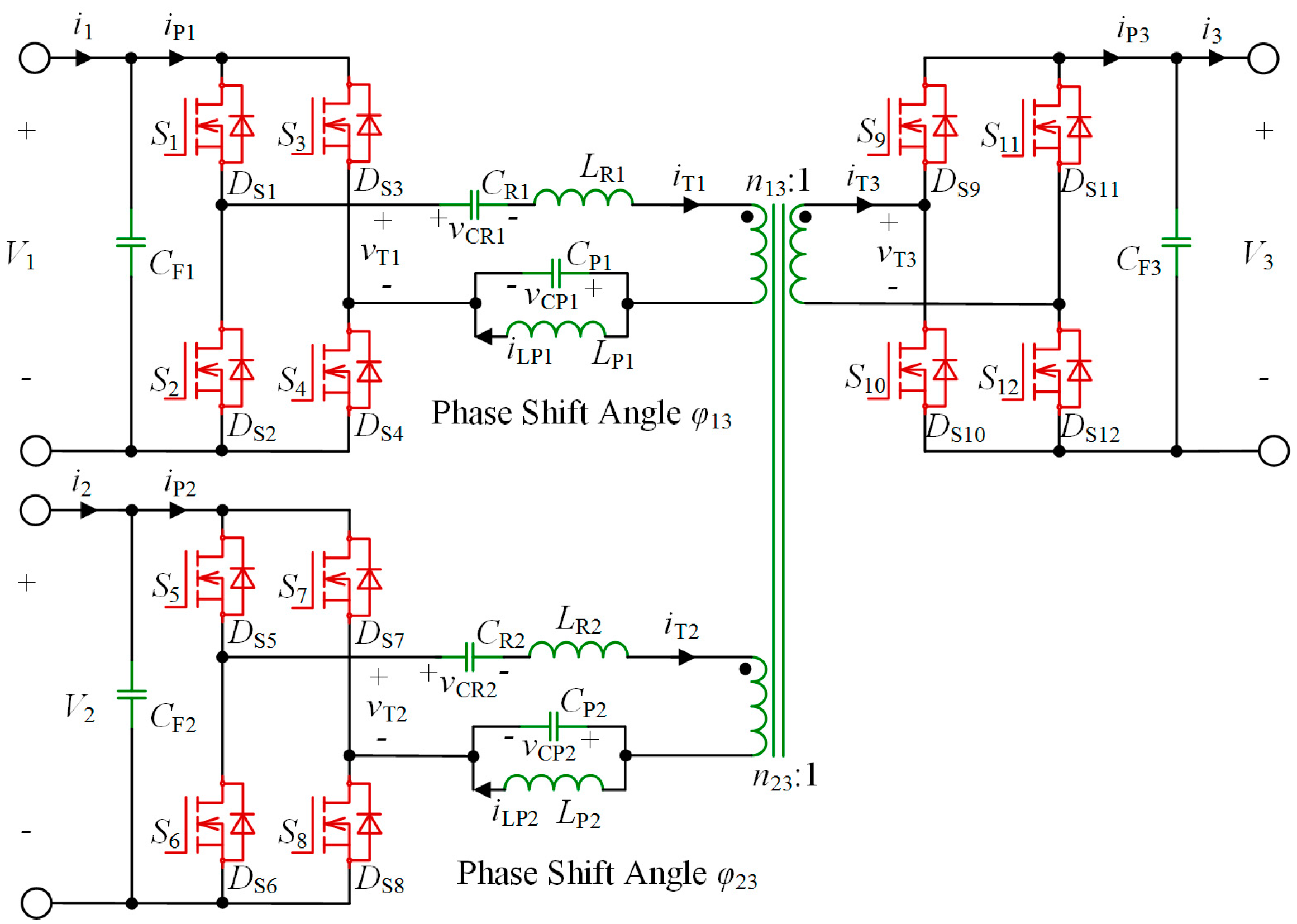
The proposed MR-TP-BDC is presented in Figure 2, and it is made up of four main parts including a three-winding transformer, three full bridges, two MR tanks and three filter capacitors CF1–CF3. Phase shift control method is implemented, the amount and direction of transmitted power is controlled by the phase shift angles. Two switches of the same bridge leg conduct complementarily with fixed duty ratio of 50%. The operating frequency fs is above the resonant frequency of MR tanks to ensure the converter works only in continuous current mode.
To simplify the analysis, we assume the voltages of three ports to be constant dc. Therefore, vT1, vT2 and vT3 are square-waves with amplitudes of ±V1, ±V2 and ±V3, respectively. The phase shift angles of port 1 and 2 are defined as ϕ13 and ϕ23, and they control the phase shifts among the square wave outputs of the three active bridges. ϕ13 and ϕ23 are defined as positive if vT1 and vT2 lead vT3, and conversely, ϕ13 and ϕ23 are considered negative.
The MR tanks are made up of CR, LR, CP and LP, and in order to simplify the parameter design, resonant parameters of port 1 and 2 are set identical. The MR tanks have two series resonant frequencies (SRFs), which are defined as fr and fr3 respectively, and a notch resonant frequency (NRF) fr2. The first SRF fr helps to deliver the fundamental component energy. To avoid additional power circulation, NRF should de designed at even times of the nominal resonant frequency fr, and 2fr is selected. The second SRF, placed at 3fr, ensures the transfer of the 3rd harmonic power and thus shows significance on circulating energy reduction and efficiency saving.
The parameters are defined as follows: V1-V3 are the voltages of three ports, vT1–vT3 are the voltages of the square wave outputs of three active bridges, i1–i3 are the currents of three ports, iT1–iT3 are the resonant currents of three ports, iP1–iP3 are the currents of three full bridges; vCR1–vCR2 are the voltages of CR1 and CR2; vCP1–vCP2 are the voltages CP1 and CP2; iLP1–iLP2 are the currents of LP1 and LP2 and P1–P3 are the power of three ports. The positive direction of each value is shown in Figure 2.
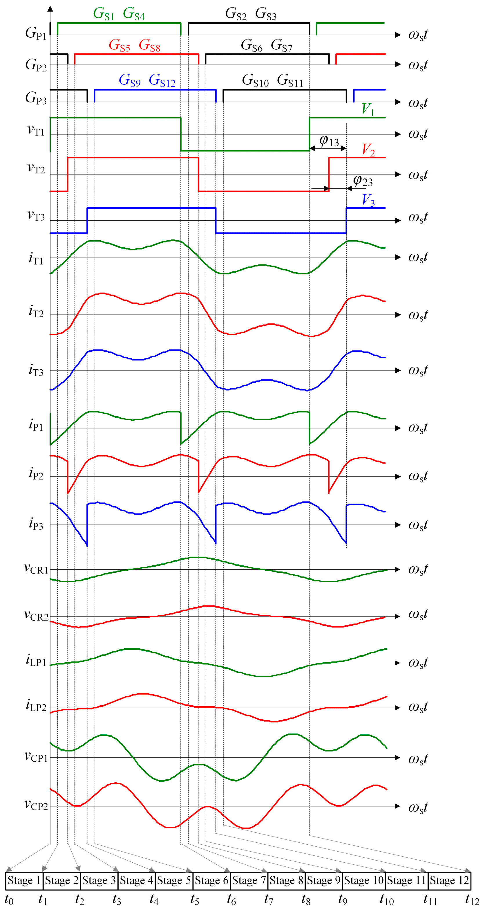
Limited by the length of the article, only the operating principle for a certain case is presented, for instance, where the power flows from port 1 and 2 to port 3. In this condition, ϕ13 > ϕ23 > 0, and the theoretical waveforms are as shown in Figure 3.
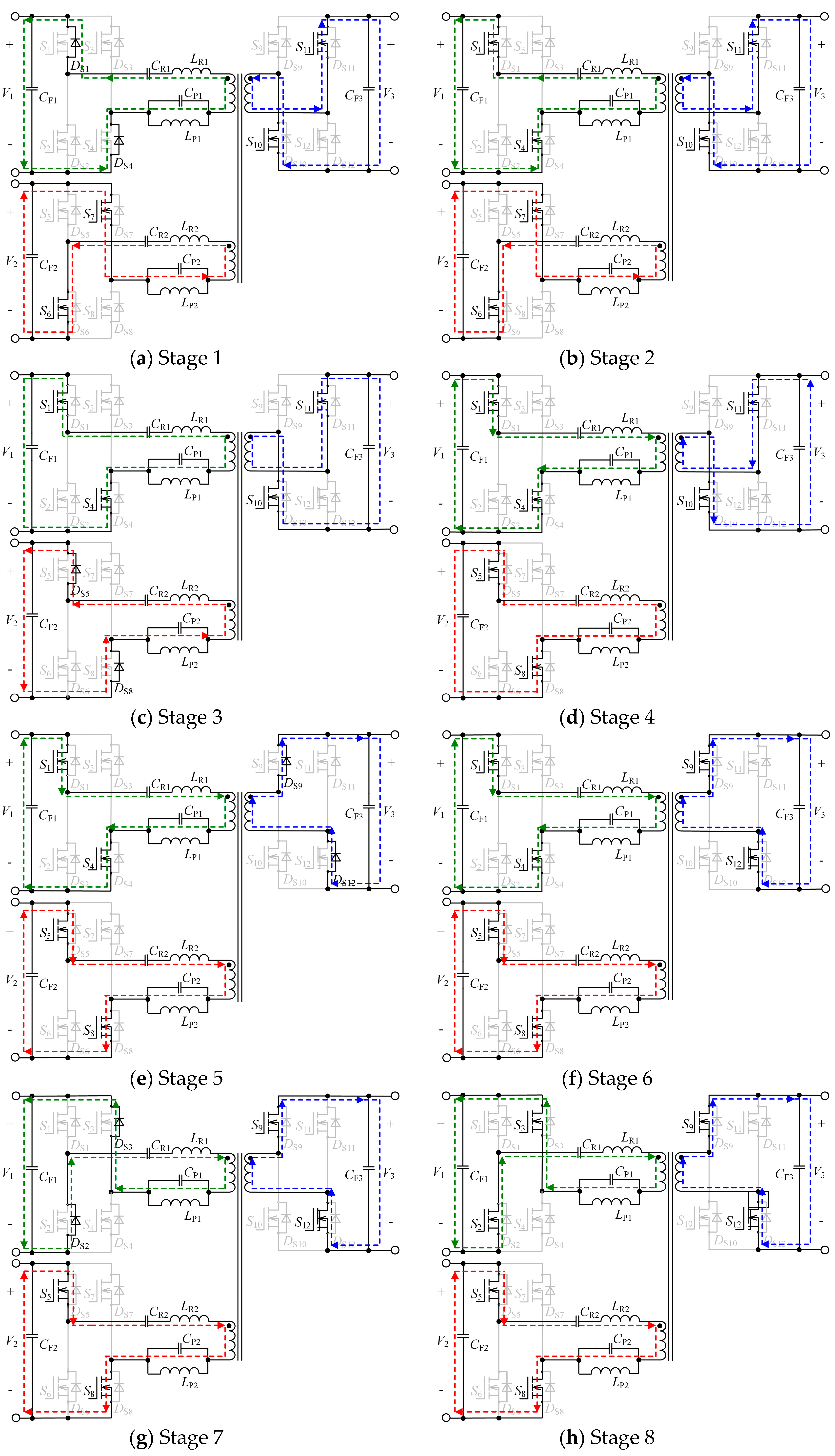
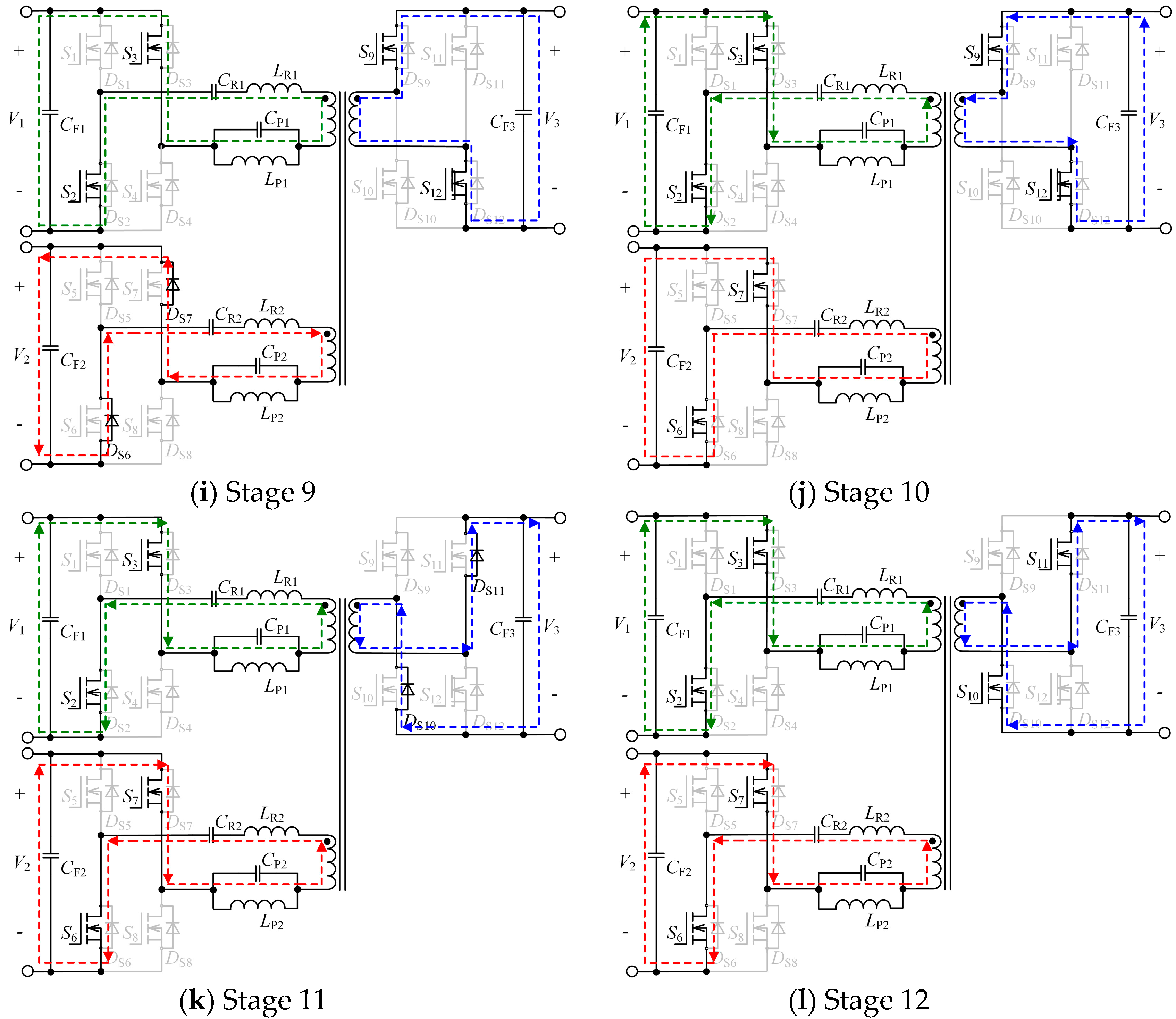
The dead time is taken into consideration, while the short intervals of the charging and discharging of switches’ parasitic output capacitors are neglected. Totally, there are 12 different intervals existing in one switching cycle, and the equivalent circuits of each stage are shown in Figure 4:
Stage 1 (t0–t1): This interval begins at the t0 when S2 and S3 are turned off, and it is dead time of port 1. During this interval, S6 and S7, S10 and S11 are on. Since iT1 is negative, it flows through Ds1 and Ds4, the anti-parallel diodes of S1 and S4. iT2 flows through S6 and S7, iT3 flows through S10 and S11. The current flow paths and directions of three ports are shown in Figure 4a. This stage ends at t1, when S1 and S4 are turned on.
Stage 2 (t1–t2): During this stage, S1 and S4, S6 and S7, S10 and S11 are on. iT1, iT2 and iT3 flow through S1 and S4, S6 and S7, S10 and S11 respectively, as shown in Figure 4b. Ds1 and Ds4 conduct prior to the main switches of S1 and S4, thus, S1 and S4 are turned on with ZVS. This stage ends at t2, when S6 and S7 are turned off.
Stage 3 (t2–t3): This stage is dead time of port 2, S1 and S4, S10 and S11 are on. iT1 and iT3 flow through S1 and S4, S10 and S11 respectively. iT2 is negative, so iT2 flows through the anti-parallel diodes of S5 and S8. The current flow paths and directions of three ports are shown in Figure 4c, while the current directions of port 1 and 3 change in this interval, so only the current paths of iT1 and iT3 are given. This interval ends at t3, when S5 and S8 are turned on.
Stage 4 (t3–t4): During this stage, S1 and S4, S5 and S8, S10 and S11 are on. iT1, iT2 and iT3 flow through S1 and S4, S5 and S8, S10 and S11 respectively. Ds5 and Ds8 conduct prior to the main switches of S5 and S8, thus, S5 and S8 are turned on with ZVS. The operating states of three ports are shown in Figure 4d. In this stage the direction of iT2 changes, so only the current path of port 2 are given. This stage ends at t4, when S10 and S11 are turned off.
Stage 5 (t4–t5): During this stage, S1 and S4, S5 and S8 are on, and this interval is dead time of port 3. iT1 and iT2 flow through S1 and S4, S5 and S8 respectively. iT3 is positive, so it flows through the anti-parallel diodes of S9 and S12. The operating states of three ports are shown in Figure 4e. This interval ends at t5, when S9 and S12 are turned on.
Stage 6 (t5–t6): During this stage, S1 and S4, S5 and S8, S9 and S12 are on. As shown in Figure 4f, iT1, iT2 and iT3 flow through S1 and S4, S5 and S8, S9 and S12 respectively. Ds9 and Ds12 conduct prior to the main switches of S9 and S12, thus, S9 and S12 are turned on with ZVS. This stage ends at t6, when S1 and S4 are turned off.
Stage 7 (t6–t7): This stage is dead time of port 1. During this interval, S5 and S8, S9 and S12 are on. Since iT1 is positive, it flows through Ds2 and Ds3, the anti-parallel diodes of S2 and S3. iT2 flows through S5 and S8, iT3 flows through S9 and S12. The current flow paths and directions of three ports are shown in Figure 4g. This stage ends at t7, when S2 and S3 are turned on.
Stage 8 (t7–t8): During this stage, S2 and S3, S5 and S8, S9 and S12 are on. As shown in Figure 4h, iT1, iT2 and iT3 flow through S2 and S3, S5 and S8, S9 and S12 respectively. Ds2 and Ds3 conduct prior to the main switches of S2 and S3, thus, S2 and S3 are turned on with ZVS. This stage ends at t8, when S5 and S8 are turned off.
Stage 9 (t8–t9): This stage is dead time of port 2. During this interval, S2 and S3, S9 and S12 are on. Since iT2 is positive, it flows through Ds6 and Ds7, the anti-parallel diodes of S6 and S7. iT1 flows through S2 and S3, iT3 flows through S9 and S12. The operating states of three ports are shown in Figure 4i, while the current directions of port 1 and 3 change in this interval, so only the current paths of iT1 and iT3 are given. This interval ends at t9, when S6 and S7 are turned on.
Stage 10 (t9–t10): During this stage, S2 and S3, S6 and S7, S9 and S12 are on. As shown in Figure 4j, iT1, iT2 and iT3 flow through S2 and S3, S6 and S7, S9 and S12 respectively. In this stage the direction of iT2 changes, so only the current path of port 2 is given. Ds6 and Ds7 conduct prior to the main switches of S6 and S7, thus, S6 and S7 are turned on with ZVS. This stage ends at t10, when S9 and S12 are turned off.
Stage 11 (t10–t11): This stage is dead time of port 3. During this interval, S2 and S3, S6 and S7 are on. Since iT3 is negative, it flows through Ds10 and Ds11, the anti-parallel diodes of S10 and S11. iT1 flows through S2 and S3, iT2 flows through S6 and S7. The operating states of three ports are shown in Figure 4k. This interval ends at t11, when S10 and S11 are turned on.
Stage 12 (t11–t12): During this stage, S2 and S3, S6 and S7, S10 and S11 are on. As shown in Figure 4l, iT1, iT2 and iT3 flow through S2 and S3, S6 and S7, S10 and S11 respectively. Ds10 and Ds11 conduct prior to the main switches of S10 and S11, thus, S10 and S11 are turned on with ZVS. This stage ends at t12, when S2 and S3 are turned off.
3. Steady-State Analysis
In this section, the steady-state analysis is conducted for the proposed isolated MR-TP-BDC, including expressions of resonant currents, voltages of resonant capacitors, power transmission among three ports and voltage gains under resistive loads.
3.1. Normalization and Definitions
To simplify the circuit analysis and parameter design, the resonant parameters of port 1 and 2 are assumed to be identical, that is CR1 = CR2 = CR, LR1 = LR2 = LR, CP1 = CP2 = CP and LP1 = LP2 = LP. Besides, to facilitate the explanation of the parameter design, all the equations presented are normalized on the basis of Equation (1):
The normalized driving frequency is shown as Equation (2), where ωs and ωr are the corresponding angular velocities of fs and fr, respectively:
The impedance of MR storage under two SRFs (fr and fr3) are 0, and impedance under NRF (fr2) is infinite. Moreover, the relationships of the three resonant frequencies are: fr2 = 2fr, fr3 = 3fr. Thus, the impedance of MR storage under fr, fr2 and fr3 are defined as Xr1, Xr2 and Xr3, and are deduced in Equation (3):
From (3), the relationship between four resonant parameters are deduced as:
The impedance of MR storage under angular velocity ω is:
Combining Equations (4) and (5), the impedance of MR storage under fs and 3fs can be expressed as Equation (6).
where Q is defined as:
3.2. Operating Characteristics with Voltage Source Load
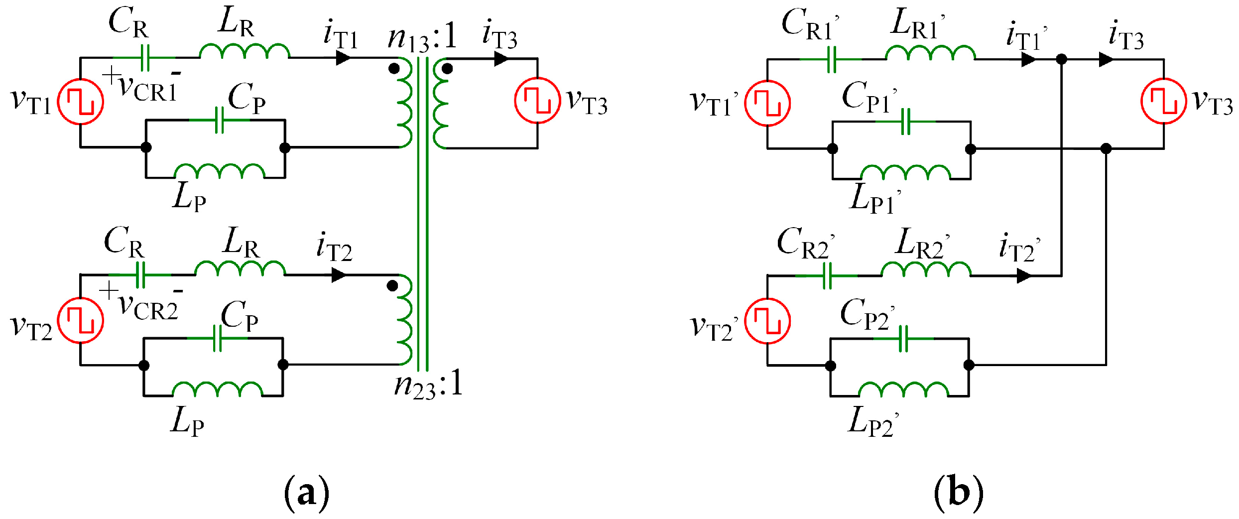
The equivalent circuit of the proposed MR-TP-BDC is presented in Figure 5a, where the three square-wave vT1, vT2 and vT3 represent the outputs of the active bridges. By transferring all parameters of port 1 and port 2 to port 3, the equivalent circuit can be further simplified as Figure 5b shows. The superscript “′” indicates the transferred parameters. On account of the complexity of MR tank, the proposed MR-TP-BDC has a plurality of resonant components and operating modes. It will be difficult to analyze the circuit with traditional time-domain analysis method. Therefore, Fourier equivalent method is adopted in the following analysis procedure. The accuracy of the calculation is verified by the experimental results.
In the proposed MR-TP-BDC, all harmonics except the fundamental and third order components of all voltages and currents are neglected. After Fourier decomposition, v′T1, v′T2 and vT3 are shown as:
M1 and M2 are the voltage gains between port1 and port 3, port 2 and port 3 respectively, and are given by Equation (9):
Assume the transformer to be ideal, and the transformer voltage is clamped by the voltage of port 3. The currents of port 1 and 2 are decided by their voltage and phase shift angles respectively. The resonance currents shown in Figure 5b are derived as:
The normalized impedance of CR under fs and 3fs are expressed as Equation (11):
By combining Equations (10) and (11), the voltages of series resonant capacitors are deduced as:
For switches in port 1, the ZVS realizing condition is that the resonant storage current lags its applied square wave voltage. For S1 and S4, ZVS will be achieved only on the condition that their currents at the conduction time are negative, while for S2 and S3, resonant current at the conduction time should be positive to guarantee ZVS operating. The ZVS constraint conditions of port 1 are expressed as Equation (13):
According to the properties of the cosine function, the ZVS constraint formulas of the four switches in port 1 are completely equivalent. As a consequence, simple analysis on the ZVS condition for S1 is enough for port 1. Similarly, ZVS conditions of S5 and S9 indicate the ZVS conditions of port 2 and 3. To sum up, the ZVS constraint expressions of three ports are shown in Equation (14):
Since the instantaneous output voltages and currents of three active bridges are shown in equations (8) and (10), respectively, the output active power of three ports are shown in Equation (15).
By substituting Equations (8) and (10) into (15), the output power of three ports are shown in Equation (16):
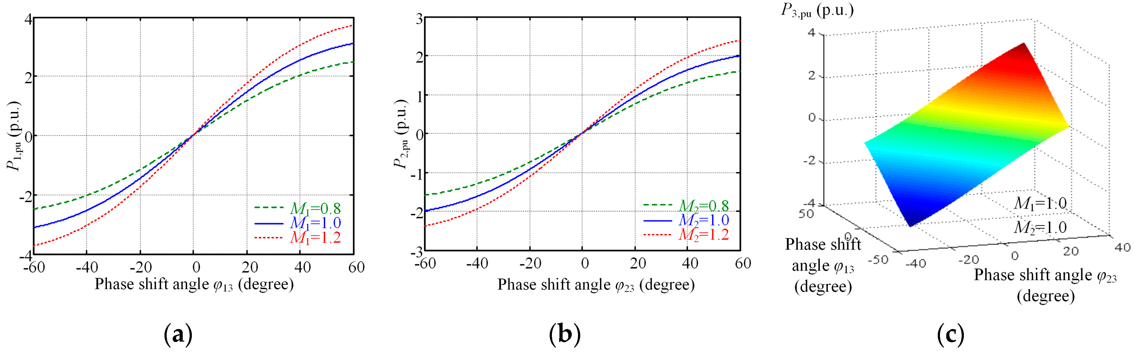
Equation (16) indicates that the powers of port 1 and port 2 are only relative to ϕ13 and ϕ23, while P3,pu are effected by both ϕ13 and ϕ23. Figure 6a shows the relationship between P1,pu and ϕ13, Figure 6b shows the relationship between P2,pu and ϕ23, while Figure 6c shows P3,pu with varying ϕ13 and ϕ23.
Equation (16) and Figure 6 indicate that when ϕ13 and ϕ23 are positive, power is transferred from port 1 and port 2 to port 3, while at the converse situation, the power flow is negative. Furthermore, the values of transferred power increases with the increment of phase shift angles.
3.3. Voltage Gain with Resistive Load
In the analysis above, the operating characteristics of the proposed converter under given port voltages are deduced. This section explains the relationship of voltage gain, power transmission and phase shift angles with a resistive load. The voltage gain analyses are divided into two cases.
In the first case, port 1 and 2 are connected to voltage sources of V1 and V2, port 3 is connected to resistive load, and the resistive value is defined as R3. At this time, the power is transferred from port 1 and port 2 to port 3, and both ϕ13 and ϕ23 are positive. The power of port 3 is P3 = V32/R3. Combing Equation (16), the power of port 3 will be derived as:
Since the base values for normalization in Equation (1) are the operating parameters of port 3, Equation (17) uses the actual electric values rather than the normalized ones. Combining (16) and (17), the output power in this condition can be expressed as Equation (18):
where Xs1 and Xs3 are the impedance values of MR tanks under fundamental frequency and third order frequency, respectively, and Xs1 = Xs1,pu × ZB, Xs3 = Xs3,pu × ZB.
In another case, port 3 is connected to a voltage source, and resistive loads R1 and R2 are connected to port 1 and 2, respectively. In this condition, power is transferred from port 3 to port 1 and 2, and both ϕ13 and ϕ23 are negative. The power of port 1 and 2 are expressed as: P1 = V12/R1 and P2 = V22/R2. By combing Equation (16), P1 and P2 are derived as:
where V1 = n13M1VB, V2 = n23M12VB. Then the voltage gains of port 1 and 2 in this condition are deduced as:
and R1,pu = R1/ZB, R2,pu = R2/ZB.
4. Design Parameter Optimization
Same as the other resonant converters, the optimization for the resonant parameters is of great importance, since the operating characteristics of the proposed converter are mainly affected by these parameters. The design requirements of the proposed converter are shown as follows:
- Port 1: V1 = 200 V, P1 = 1000 W;
- Port 2: V2 = 160 V, P2 = 500 W;
- Port 3: V3 = 400 V, P3 = 1500 W.
The parameters which need to be optimized include the transformer ratio, values of resonant components and driving frequency. The optimization objectives are ZVS range, peak value of resonant currents, voltage stress of resonant capacitors and cutoff current of switches. And the parameters are optimized in detail in the following.
Since the voltage of transformer is clamped by the voltage of port 3, there is no direct power interaction between port 1 and port 2. It is feasible to decompose the proposed MR-TP-BDC into two single input MR-BDCs, and the design principles of port 1 and port 2 are identical. To simplify the analysis, the operating characteristics of single input MR-BDC are analyzed in this section.
4.1. Transformer Ratio Optimization
The transformer turn ratio affects voltage gain M1 and M2 as shown in Equations (8) and (9). Furthermore, Equation (14) indicates the voltage gains directly influence the ZVS realization ranges of three ports. Since there is no direct power interaction between port 1 and port 2, the ZVS realization ranges of port 1 and 3 under single input condition are efficient to analyze the relationship between voltage gain and ZVS region.
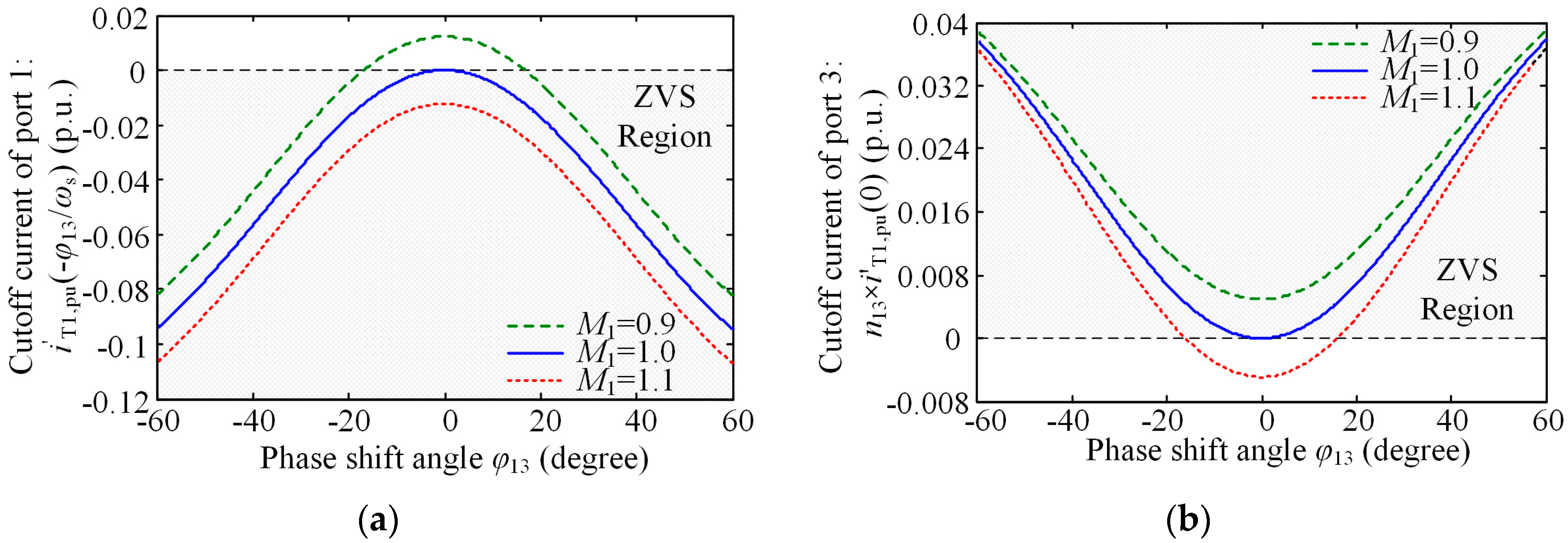
The ZVS constraint conditions of three ports are given in (14). In the condition of single input, the ZVS realization conditions of port 1 and 3 are i′T1,pu(−ϕ13/ωs) < 0 and i′T1,pu(0) > 0 respectively. The ZVS regions of port 1 and port 3 under varying M1 are shown in Figure 7a,b.
Figure 7a indicates that when M1 is less than or equal to 1, all the switches in port 1 can realize ZVS. When M1 is greater than 1, switches in port 1 cannot realize ZVS unless ϕ13 (output power) is greater than a certain value. While for port 3 shown in Figure 7b, conditions are exactly contrary to port 1. When M1 is less than 1, switches in port 3 can only realize ZVS only when the phase shift angel is greater than a certain value. It can be obtained that, the ZVS realization regions of port 1 and port 3 change reversely under varying M1, so during the design process, M1 should be as close to 1 as possible, and M1 = 1 is the best choice to achieve ZVS for all the switches of port 1 and 3.
Conditions of port 2 are exactly the same with port 1, and M1 = M2 = 1 are the optimal voltage gains to guarantee ZVS operation of all switches of proposed isolated MR-TP-BDC. According to the given voltages of three ports and voltage gains, turn ratios of transformer are defined as: n13:n23:1 = 0.5:0.4:1.
4.2. Resonant Components Optimization
The MR storage in the proposed converter consists of four resonant elements: resonant capacitors CR and CP, resonant inductors LR and LP. While there are constraint relations between the four resonant elements as shown in Equation (4). This will greatly reduce the difficulty of parameters design. In the following parameters design process, LP is selected as the optimization variable. In the considered single-input converter, P1,pu = P3,pu, iT1,pu(t) = i′T1,pu(t)/n13, i′T1,pu(−ϕ13/ωs) = −iT3,pu(0).
With given voltage gains, resonant parameters and driving frequency, the phase shift angle ϕ13, which can provide certain P1,pu, will be derived by solving Equation (16). Then substitute ϕ13 into (10), the corresponding cutoff current is expressed as iT1,pu(-ϕ13/ωs) = i′T1,pu(-ϕ13/ωs)/n13. Through using the function of seeking maximum value in MATLAB (Mathworks, Natick, MA, USA), the peak value of resonant current is acquired, and expressed as IT1max,pu = max[i′T1,pu(t)]/n13.
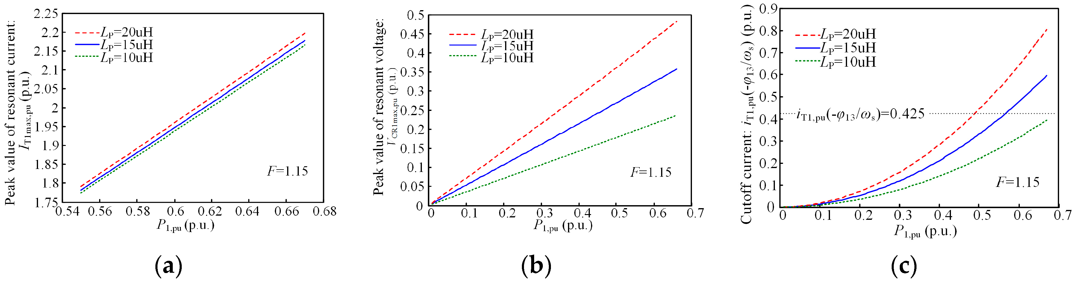
Figure 8 shows the peak value of resonant current IT1max,pu, peak value of resonant capacitor voltage VCR1max,pu and cutoff current of port 1 iT1,pu(−ϕ13/ωs) versus P1,pu under varying LP. In the designing process, P1 = 1000 W, PB = P3 = 1500 W, therefore, the maximum value of P1,pu is 0.67.
Figure 8 indicates that the peak value of resonant current, peak value of resonant capacitor voltage and cutoff current increase LP increases. From the point of view of reducing the power loss of proposed MR-TP-BDC, LP should be chosen as small as possible. Meanwhile, the converter will lose its ZVS property when the cutoff current is very small. In this condition, the energy stored in the MR storage is not enough to get the output capacitor of metal-oxide-semiconductor field effect transistor (MOSFET) completely discharged. Therefore, the critical cutoff current value, which guarantee ZVS of converter, should be deduced.
The analysis above indicates that M1 = M2 = 1 are the optimal voltage gains to guarantee ZVS operation of all switches of proposed isolated MR-TP-BDC. Equation (14) shows the ZVS constraint expressions of three ports. While, the aforementioned conclusions are all based on ideal MOSFETs and the output capacitors of MOSFETs are neglected. However, in the actual experimental processes, the energy stored in the resonant tanks must be enough to get the output capacitors fully discharged during the dead time. Hence the cutoff current must be high enough to achieve ZVS condition.
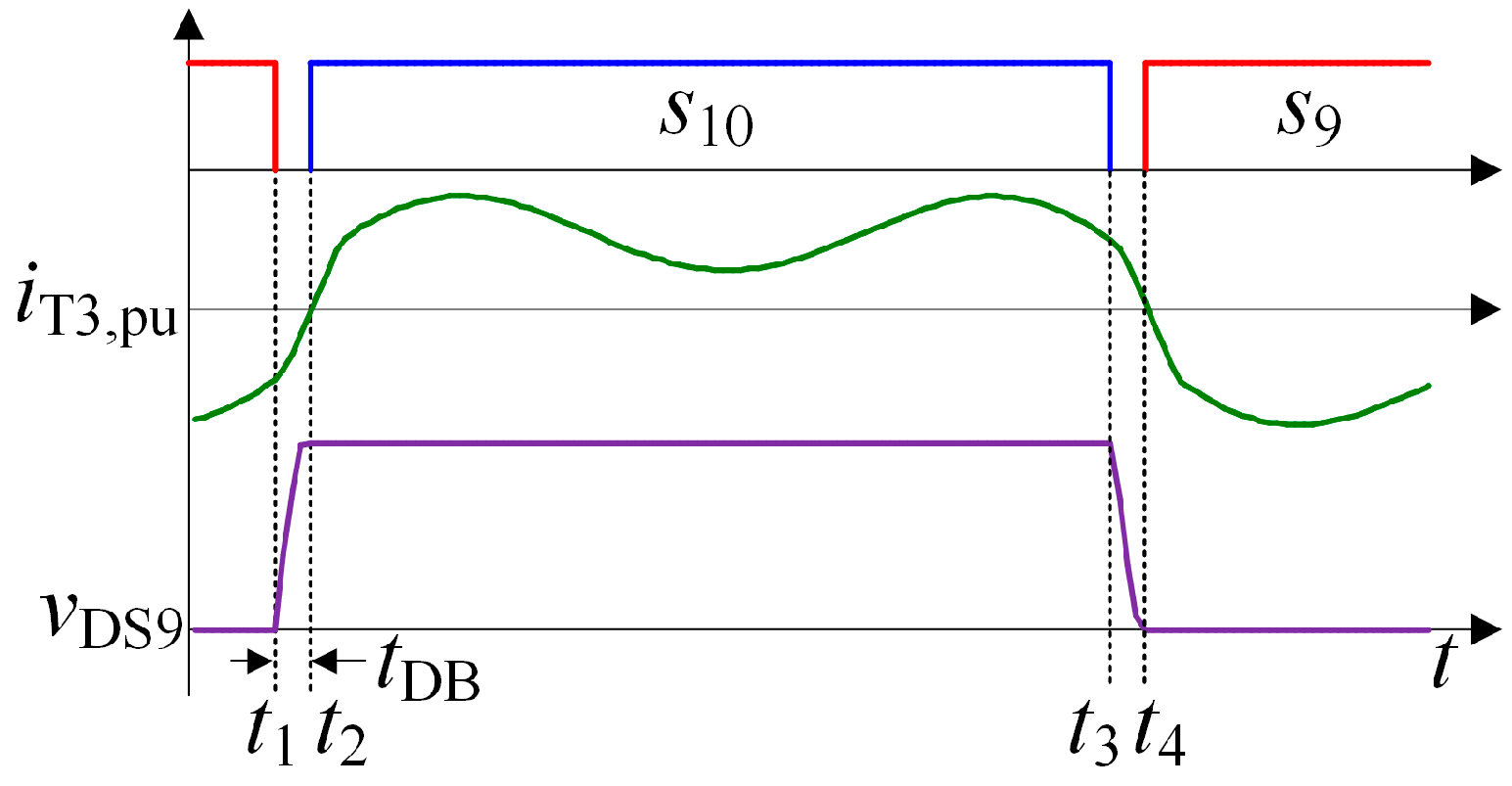
When the MOSFETs are turned off, their drain-source voltages are equal to their respective port voltages. On the basis of the utilized design method, port 3 has the highest voltage of 400 V, and thus the output capacitors of MOSFETs in ports 3 store most energy in their cut-off stage. Besides, port 3 has the highest voltage, which means a smaller winding current. Hence the ZVS realization conditions of switches in port 3 are the most difficult. Moreover, the discharging current of the switch parasitic output capacitor of port 3 decreases when power is transferred from port 3 to port 1. Figure 9 shows the critical ZVS condition of switches in port 3 under the most severe situation. In this condition, output capacitor of S9 is just completely discharged when the resonant current decreases to zero. The corresponding cutoff current is defined as Itomin, which is the minimum cutoff current to guarantee ZVS operation of port 3.
In Figure 9, t1–t2 and t3–t4 are the dead time of port 3. At t3, S10 is turned off, and the output capacitors of S9 and S10 begin to get discharged and charged, respectively. The values of charging and discharging current of S9 and S10 are all iT3,pu(t)/2. During t3–t4, iT3,pu(t) is assumed to be decrease linearly. According to the discharging formula of capacitor, the voltage changing process of S9 can be expressed as:
Thus, the critical ZVS condition of S9 shown in Figure 9 is derived as:
where Coss is the parasitic output capacitor of switches and tDB represents the dead time. For the MOSFET selected in this article, the value of parasitic output capacitor under 0–400 V voltage range is 150 pF. The dead time is chosen as 200 nS. By substituting Coss and tDB into (22), Itomin is derived as 1.2 A. Since the power distribution among three ports are: P1:P2:P3 = 2:1:3, then the minimum cutoff current assigned to port 1 is approximated as:
To ensure the converter efficiency under rated power state, the cutoff current should be minimized on the premise of realizing ZVS. Figure 8c shows that, when LP = 10 μH, the cutoff current of port 1 is iT1,pu(–ϕ13/ωs) = 0.40 and it doesn’t satisfy the ZVS constraint shown in (23). When LP = 15 μH, iT1,pu(–ϕ13/ωs) = 0.59, ZVS operation can be guaranteed. What’s more, the peak value of resonant current and resonant capacitor voltage are IT1max,pu = 2.18 and VCR1max,pu = 0.37 respectively, and both of them are in a reasonable range. To sum up, LP = 15 μH is selected in the proposed isolated MR-TP-BDC.
4.3. Driving Frequency Optimization
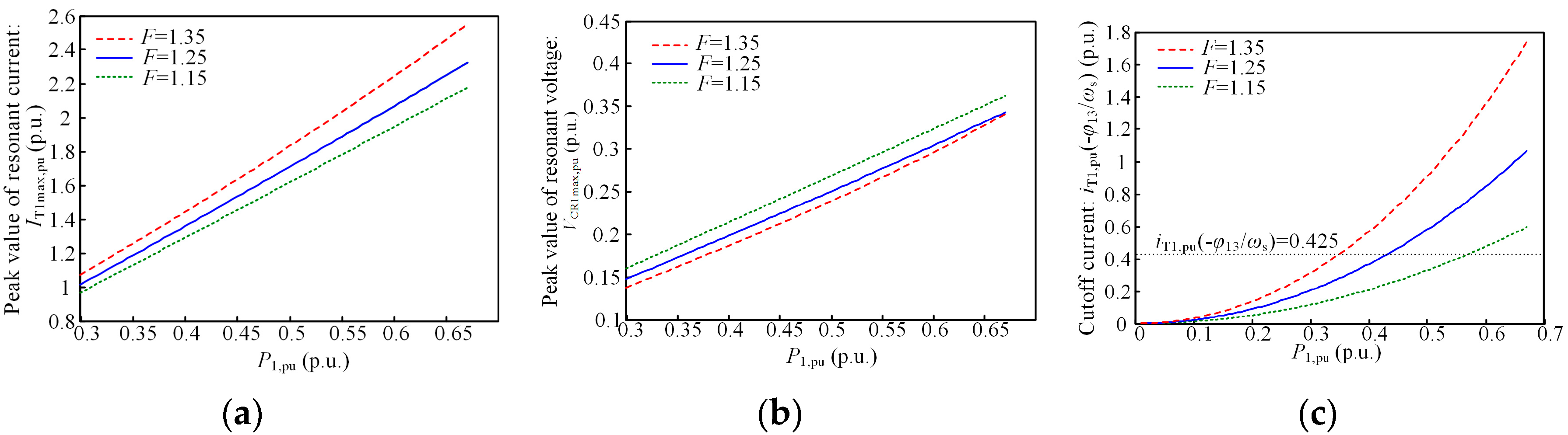
Equation (6) indicates that the MR storage impedances under fundamental and third order frequencies change under varying F. The operating characteristics of the proposed converter should be compared under different F. The peak value of resonant current IT1max,pu, peak value of resonant capacitor voltage VCR1max,pu and cutoff current of port 1 iT1,pu(–ϕ13/ωs) are plotted by MATLAB and are shown in Figure 10.
Figure 10 shows that the effects of F on IT1max,pu and VCR1max,pu are small and can be neglected. While the cutoff current iT1,pu(–ϕ13/ωs) increases obviously with the increase of F. The ZVS constraint deduced in 4.2 is also shown in Figure 10c. If F = 1.15 is adopted in the full load range, ZVS properties will be missed. Therefore, to ensure optimal efficiency under full load range, driving frequency should increase with the decrease of power level. Values of F under the rated and half load conditions are selected as 1.15 and 1.35, respectively.
5. Experimental Results
To verify the feasibility of the proposed topology and the accuracy of the theoretical analysis, a 1.5 kW prototype is built and tested in the laboratory. The MOSFETs adopted in the system is C3M0065090D manufactured by CREE (Durham, NC, USA). The DSP TMS320F28379D from Texas Instruments (Dallas, TX, USA) is employed as the digital controller. The optimized parameters of the proposed converter are selected and shown in Table 1. In the experiments P1, P2 and P3 are defined as positive when power flows from port 1 and port 2 to port 3, and vice versa.
5.1. Forward Operating Mode
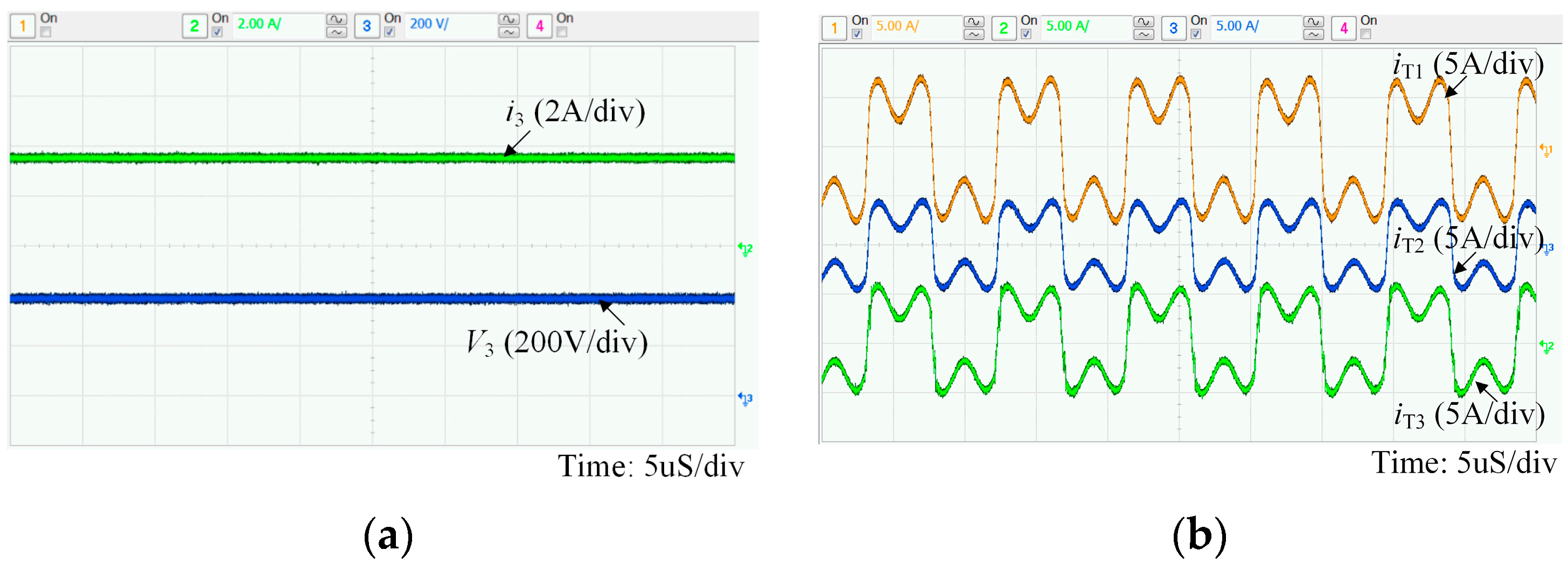
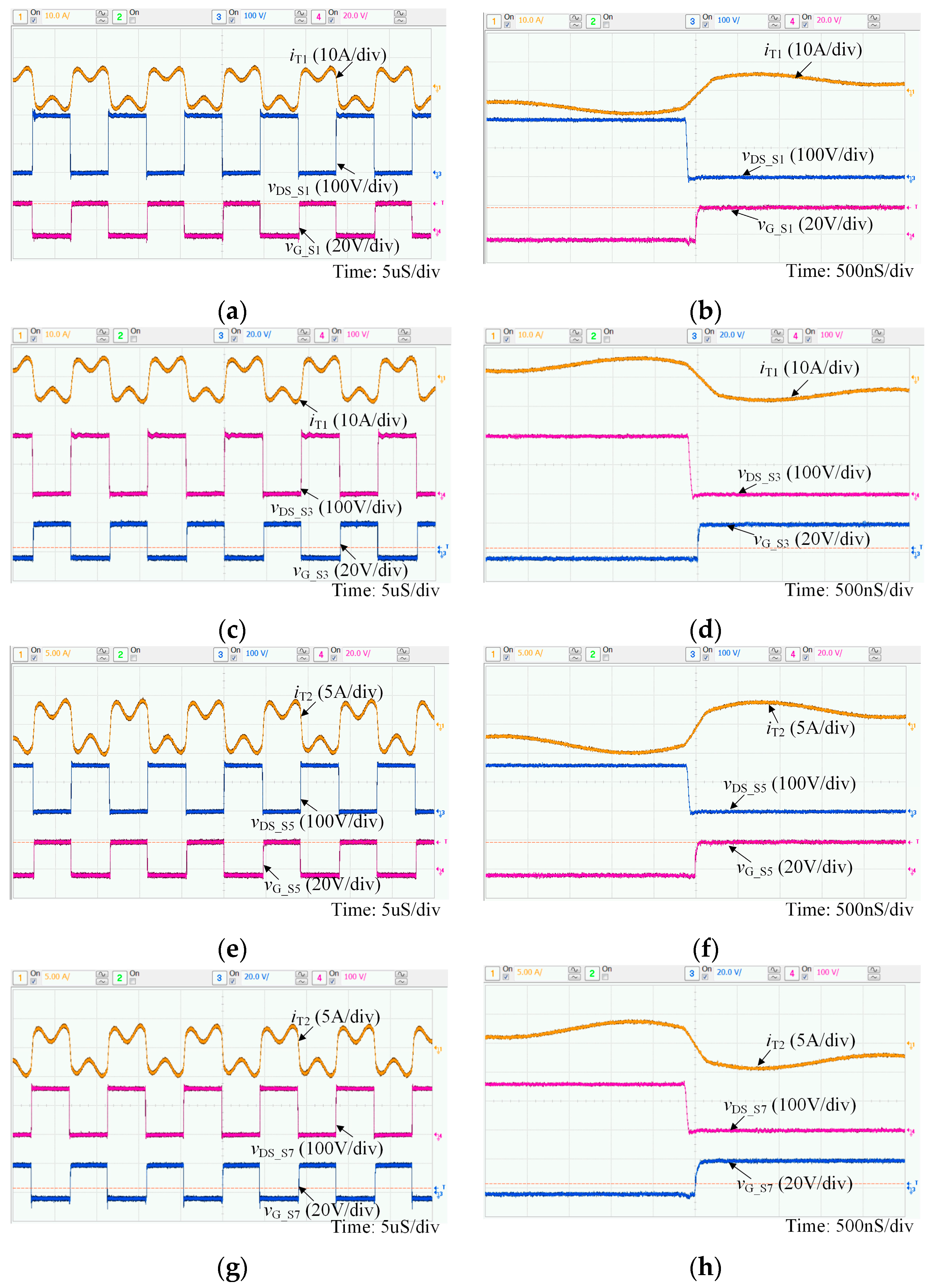
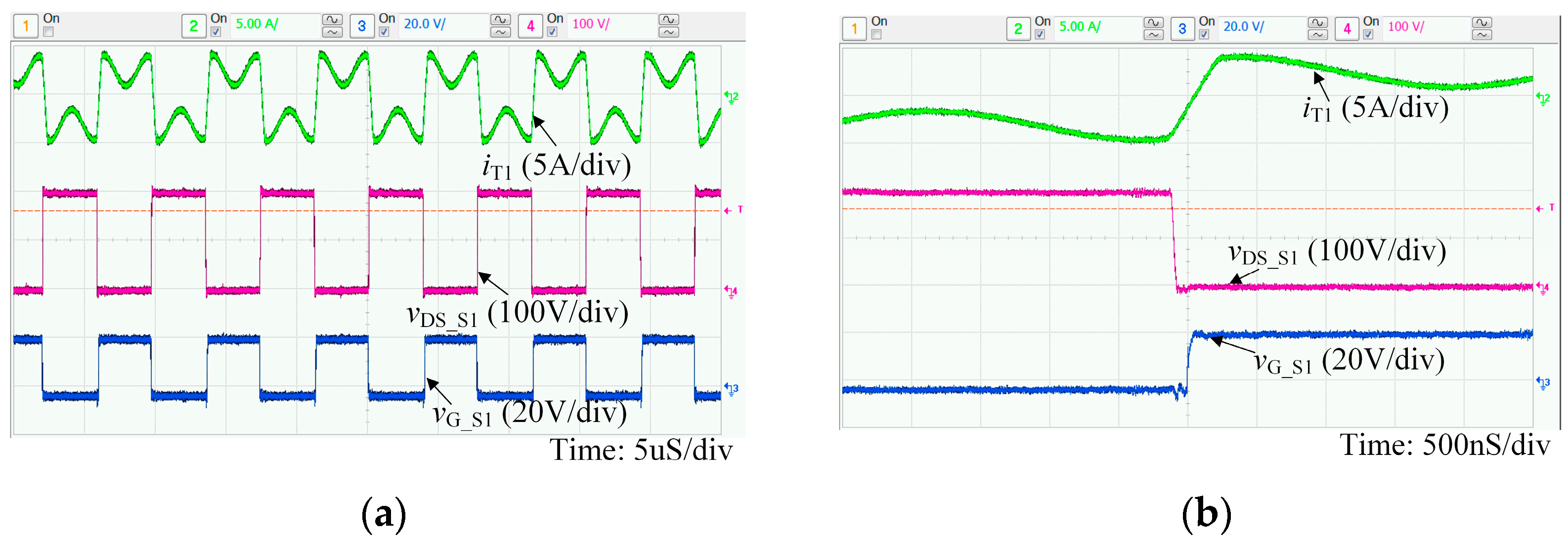
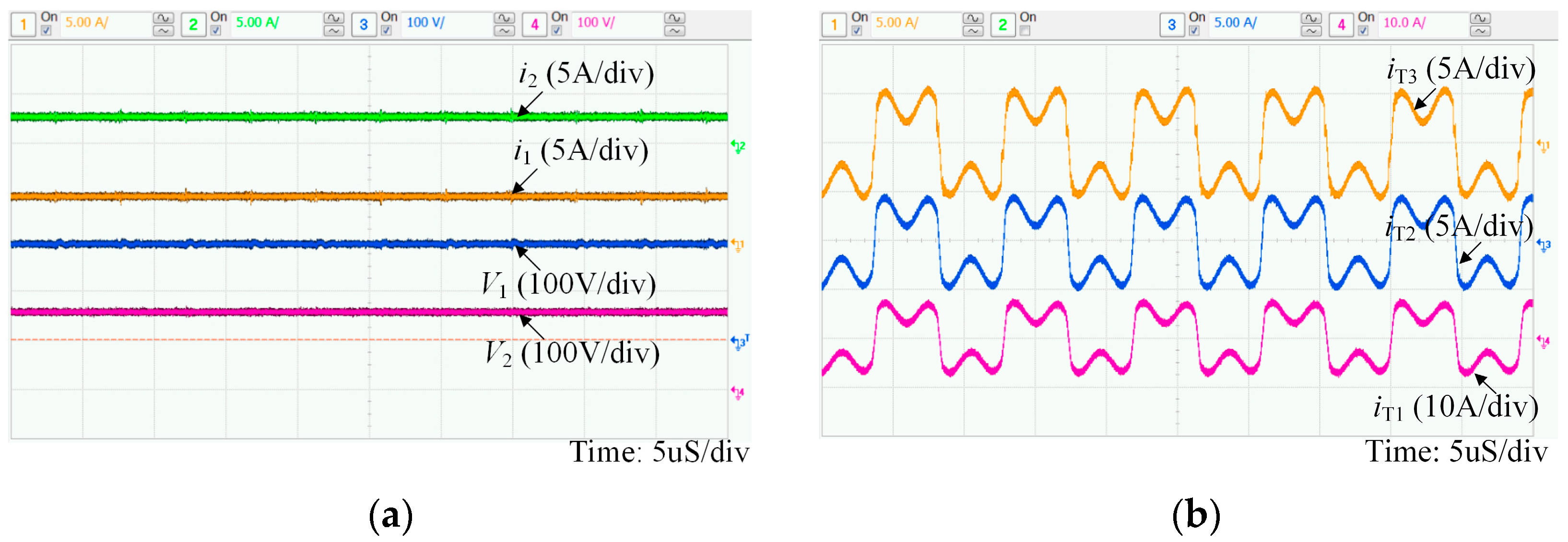
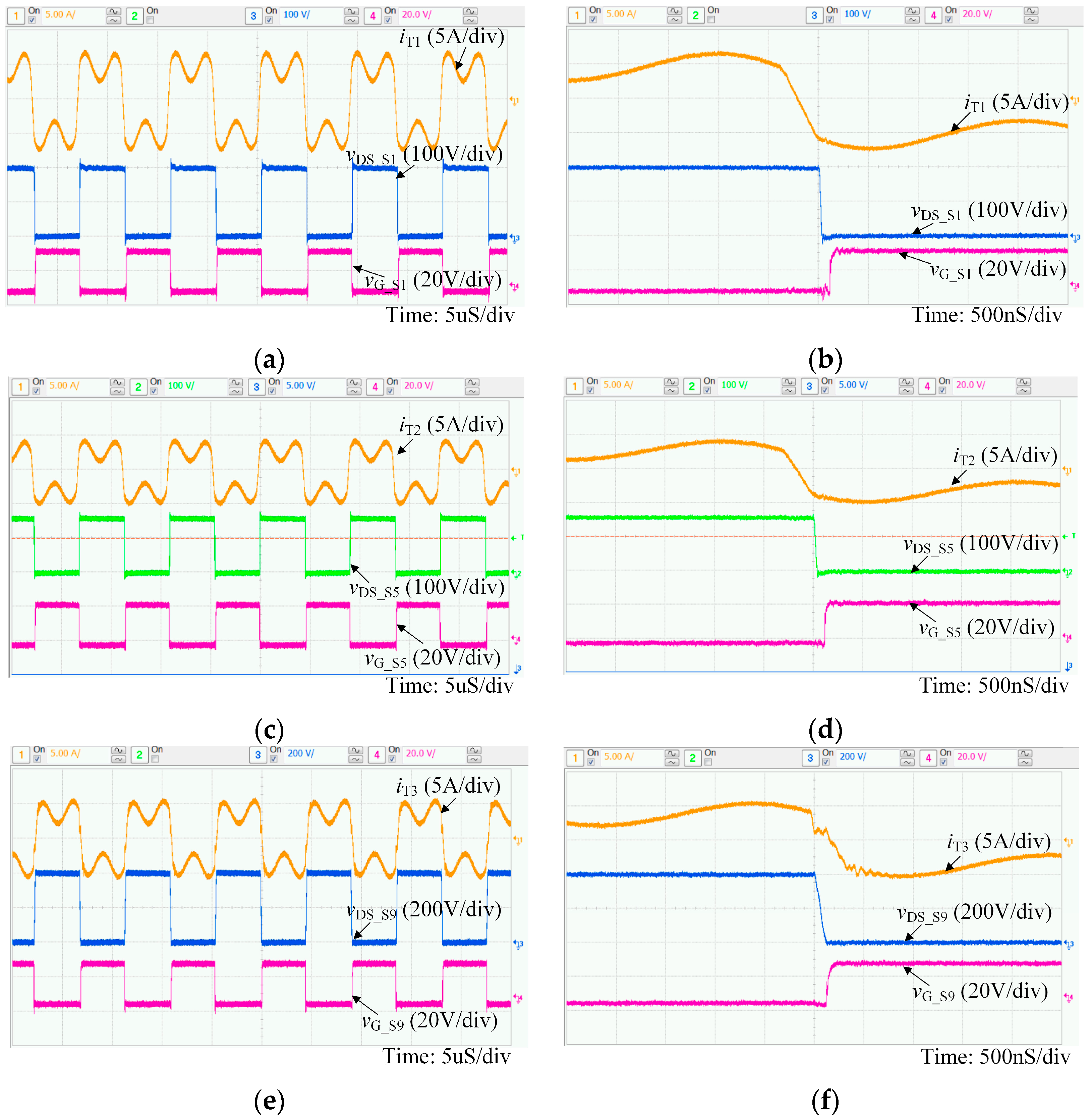
Experimental results under rated and half load positive conditions are evaluated. In the rated positive mode, port 1 and 2 are connected to voltage sources of 200 V and 160 V, respectively. A resistive load of 106 Ω is connected to port 3. In this experiment, power flows from port 1 and 2 to port 3, vT1 and vT2 lead vT3. The specific data of this experiment are given as follows: input voltage V1 = 200 V, V2 = 160 V; output voltage V3 = 398 V; driving frequency fs = 110 kHz, ϕ13 = 14.2°, ϕ23 = 11.1°; P1 = 1015 W, P2 = 497 W, P3 = 1455 W. The efficiency is 96.2%.
Waveforms of output voltage and current of port 3 are shown in Figure 11a. iT1, iT2 and iT3 are currents of three transformer windings and are presented in Figure 11b. Figure 12a–d show the operating waveforms of port 1, such as iT1, and the drain-source voltages and the driving signals of S1 and S3 vDS_S1, vG_S1, vDS_S3 and vG_S3. Figure 12e–h and Figure 12i–l show waveforms of port 2 and port 3 respectively. Figure 12b,d,f,h,j,l are zoomed-in versions of Figure 12a,c,e,g,i,k. It can be obtained from the zoom-in figures that the drain-source voltages of MOSFETs decrease to zero before their driving signals turn to positive. Furthermore, vG_S1 and vG_S5 turn positive when iT1 and iT2 are negative, vG_S3 and vG_S7 turn positive when iT1 and iT2 are positive. vG_S9 turns positive when iT3 is positive, and vG_S11 turns positive when iT3 is negative. The above-mentioned facts prove that S1 and S3 of port 1, S5 and S7 of port 2 and S9 and S11 realize ZVS successfully, which means all the three-port switches achieve the desirable ZVS feature.
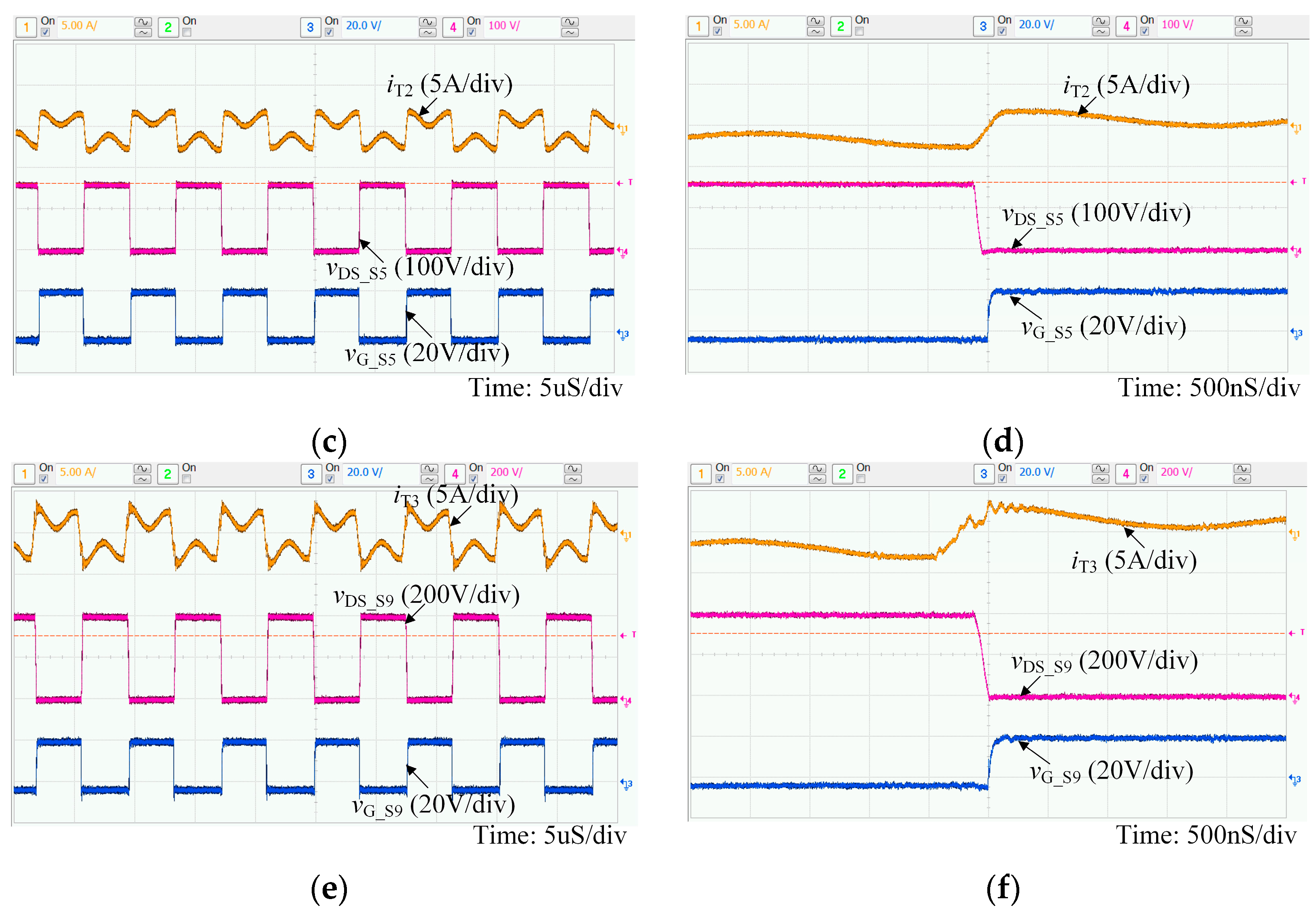
Figure 13 and Figure 14 show waveforms under half load positive mode. In this condition, voltage sources of 200 V and 160 V are supplied to port 1 and port 2, respectively. The load resistance connected to port 3 is 213 Ω. In this experiment, output voltage V3 = 399V; driving frequency fs = 130 kHz, ϕ13 = 15.8°, ϕ23 = 10.3°; P1 = 549 W, P2 = 230 W, P3 = 747 W; the efficiency is 95.8%.
Waveforms of output voltage and current of port 3 are shown in Figure 13a. Figure 13b shows waveforms of three transformer windings. Figure 14a,b, Figure 14c,d and Figure 14e,f demonstrate waveforms of port 1, port 2 and port 3. Like the experimental results shown in Figure 12, ZVS is achieved for all switches of the three ports.
5.2. Reverse Operating Mode
In the negative operating mode, 400 V voltage source is supplied to port 3 and resistive loads are connected to port 1 and port 2. Power is transferred from port 3 to port 1 and port 2, and both ϕ13 and ϕ23 are negative. Experimental results under rated and half load conditions are illustrated.
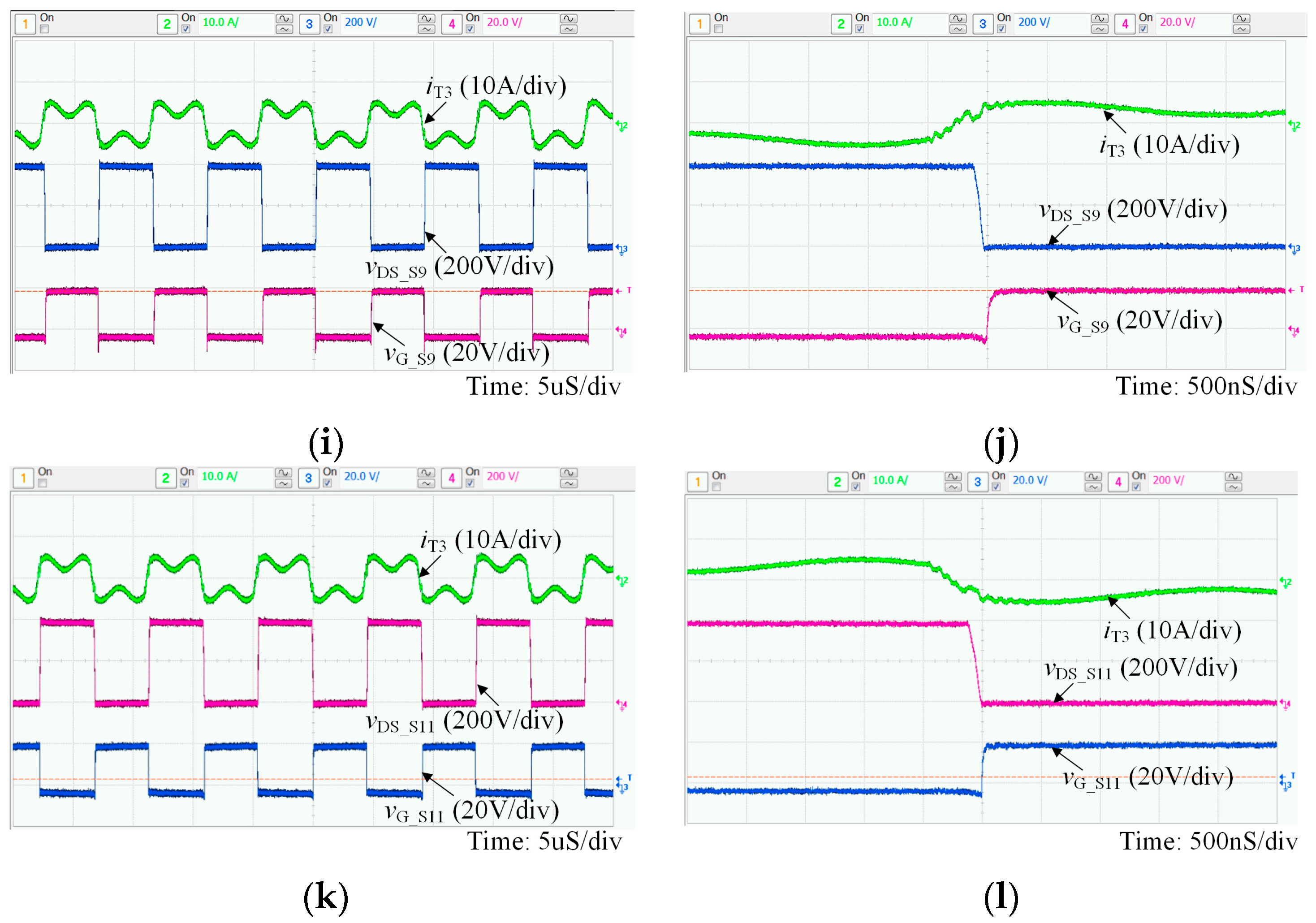
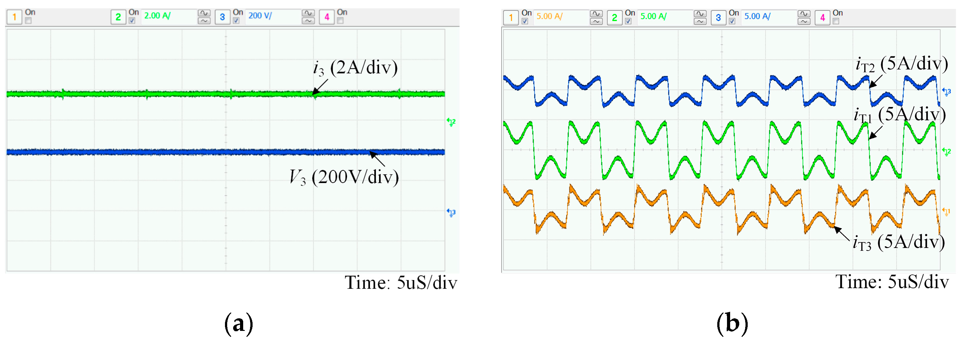
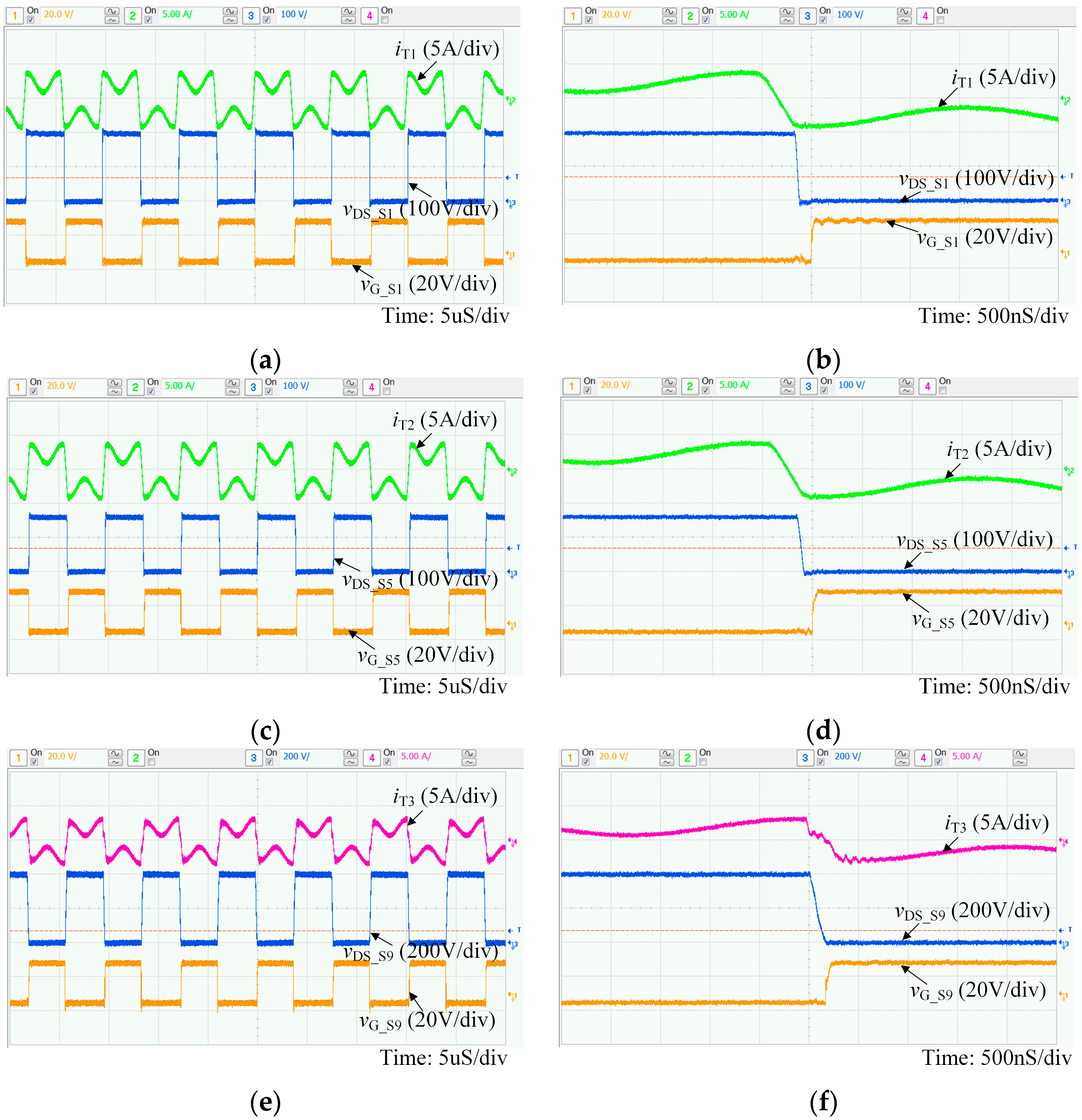
Under the rated power condition, resistances of port 1 and port 2 are 40 Ω and 50 Ω, respectively. The experimental results are listed as: output voltages V1 = 198 V, V2 = 159 V; driving frequency fs = 110 kHz, ϕ13 = −13.9°, ϕ23 = −11.4°; P1 = −965 W, P2 = −502 W, P3 = −1520 W; efficiency is 96.5%.
Figure 15a gives the waveforms of output voltage and current of port 1 and 2. Figure 15b shows the waveforms of resonant currents of three ports.
Figure 16a demonstrates iT1, vDS_S1 and vG_S1 of port 1. Figure 16c illustrates iT2, vDS_S5 and vG_S5 of port 2. Figure 16e shows iT3, vDS_S9 and vG_S9 of port 3. Figure 16b,d,f are zoomed-in waveforms of Figure 16a,c,e. The waveforms of three ports are consistent with the analysis above, and ZVS is achieved for all MOSFETs of the three ports.
Under the half power condition, resistances of port 1 and port 2 are 80 Ω and 100 Ω, respectively. The experimental results are listed as: output voltages V1 = 197 V, V2 = 159 V; driving frequency fs = 130 kHz, ϕ13 = −15.0°, ϕ23 = −11.3°; P1 = −484 W, P2 = −250 W, P3 = −764 W; efficiency is 96.0%.
Waveforms of output voltage and current of port 1 and 2 are shown in Figure 17a. Figure 17b shows the waveforms of three transformer windings. The waveforms illustrated in Figure 18 are same those in Figure 16. ZVS is achieved for all the MOSFETs.
The comparisons of phase shift angles obtained from theoretical calculation and experiment are given in Table 2. It can be seen that all the values match reasonably close to each other, and this proves the accuracy of the theoretical analysis.
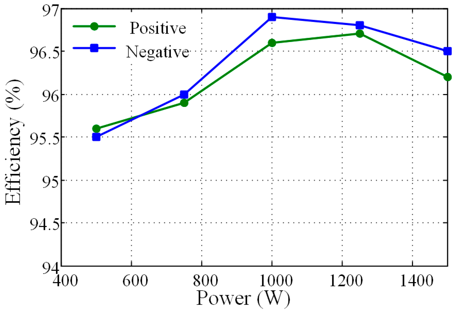
Finally, the measured efficiency curves under positive and negative conditions is shown in Figure 19. The efficiency under rated bidirectional conditions are 96.2% and 96.5%, respectively. The highest efficiency under forward condition is 96.7% at 1.25 kW, and 96.9% under 1 kW in reverse mode. Furthermore, when the power is above 0.5 kW, the efficiencies of both directions are higher than 95.5%. The proposed converter is proved to have high efficiency within entire load range.
6. Conclusions
In this paper, a three-port LCLC multi-resonant bidirectional DC-DC converter is developed. Through parameter design, the LCLC possesses two SRFs (fr and 3fr) and a NRF (2fr). Hence, the energy of first and third orders can be delivered through the MR tank, and circulating energy of the resonant tanks is reduced. What’s more, by adjusting the driving frequency under different load conditions, ZVS characteristics for all three-port switches are guaranteed among entire load range. Besides, a design procedure with normalized variables is presented. At last, a 1.5 kW prototype is implemented to validate the feasibility and practicability of the proposed converter. Experimental results indicate that the proposed converter presents high efficiency within whole load range. When the power is above 0.5 kW, the bidirectional efficiencies maintains as high as over 95.5%, and the highest efficiencies under forward and reverse conditions are 96.7% and 96.9% respectively.
Acknowledgments
This research was supported by the National High Technology Research and Development Program of China (863 Program) (Grant: 2015AA050603) and supported by Tianjin Municipal Science and Technology Commission (Grant: 14ZCZDGX00035). The authors would also like to thank the anonymous reviewers for their valuable comments and suggestions to improve the quality of the paper.
Author Contributions
Cheng-Shan Wang, Wei Li and Yi-Feng Wang designed the main parts of the study, including the circuit simulation model, topology innovation and simulation development. Fu-Qiang Han and Bo Chen helped in the hardware development and experiment.
Conflicts of Interest
The authors declare no conflict of interest.
References
- Kang, E.C.; Lee, E.J.; Ghorab, M.; Yang, L.; Entchev, E.; Lee, K.-S.; Lyu, N.-J. Investigation of energy and environmental potentials of a renewable trigeneration system in a residential application. Energies 2016, 9, 760. [Google Scholar] [CrossRef]
- Pérez-Ortiz, M.; Jiménez-Fernández, S.; Gutiérrez, P.; Alexandre, E.; Hervás-Martínez, C.; Salcedo-Sanz, S. A review of classification problems and algorithms in renewable energy applications. Energies 2016, 9, 607. [Google Scholar] [CrossRef]
- Kim, J.Y.; Kim, H.M.; Kim, S.K.; Jeon, J.H.; Choi, H.K. Designing an energy storage system fuzzy pid controller for microgrid islanded operation. Energies 2011, 4, 1443–1460. [Google Scholar] [CrossRef]
- Hu, J.; Cheng, K.W.E. Predictive control of power electronics converters in renewable energy systems. Energies 2017, 10, 515. [Google Scholar] [CrossRef]
- Xu, Q.; Hu, X.; Wang, P.; Xiao, J.; Tu, P.; Wen, C.; Lee, M.Y. A Decentralized Dynamic Power Sharing Strategy for Hybrid Energy Storage System in Autonomous DC Microgrid. IEEE Trans. Ind. Electron. 2016, 64, 5930–5941. [Google Scholar] [CrossRef]
- Kollimalla, S.K.; Mishra, M.K.; Ukil, A.; Gooi, H.B. DC Grid Voltage Regulation Using New HESS Control Strategy. IEEE Trans. Sustain. Energy 2016, 8, 772–781. [Google Scholar] [CrossRef]
- Zhang, N.; Sutanto, D.; Muttaqi, K.M. A review of topologies of three-port DC–DC converters for the integration of renewable energy and energy storage system. Renew. Sustain. Energy Rev. 2016, 56, 388–401. [Google Scholar] [CrossRef]
- Wu, H.; Sun, K.; Ding, S.; Xing, Y. Topology derivation of nonisolated three-port dc–dc converters from DIC and DOC. IEEE Trans. Power Electron. 2013, 28, 3297–3307. [Google Scholar] [CrossRef]
- Zhu, H.; Zhang, D.; Zhang, B.; Zhou, Z. A nonisolated three-port dc–dc converter and three-domain control method for PV-battery power systems. IEEE Trans. Ind. Electron. 2015, 62, 4937–4947. [Google Scholar] [CrossRef]
- Chien, L.J.; Chen, C.C.; Chen, J.F.; Hsieh, Y.-P. Novel Three-Port Converter with High-Voltage Gain. IEEE Trans. Power Electron. 2014, 29, 4693–4703. [Google Scholar] [CrossRef]
- Qian, Z.; Rahman, O.A.; Al-Atrash, H.; Batarseh, I. Modelling and control of three-port DC/DC converter interface for satellite applications. IEEE Trans. Power Electron. 2010, 25, 637–649. [Google Scholar] [CrossRef]
- Wu, H.; Chen, R.; Zhang, J.; Xing, Y.; Hu, H.; Ge, H. A family of three-port half-bridge converters for a stand-alone renewable power system. IEEE Trans. Power Electron. 2011, 26, 2697–2706. [Google Scholar] [CrossRef]
- Hu, Y.; Xiao, W.; Cao, W.; Ji, B.; Morrow, D.J. Three-Port DC–DC Converter for Stand-Alone Photovoltaic Systems. IEEE Trans. Power Electron. 2015, 30, 3068–3076. [Google Scholar] [CrossRef]
- Sun, X.; Shen, Y.; Li, W. A Novel LLC Integrated Three-port DC-DC Converter for Stand-alone PV/Battery System. In Proceedings of the 2014 IEEE Conference and Expo Transportation Electrification Asia-Pacific (ITEC Asia-Pacific), Beijing, China, 31 August–3 September 2014; pp. 1–6. [Google Scholar]
- Song, Y.; Wang, B. Survey on reliability of power electronic systems. IEEE Trans. Power Electron. 2013, 28, 591–604. [Google Scholar] [CrossRef]
- Yang, S.; Bryant, A.; Mawby, P.; Xiang, D.; Ran, L.; Tavner, P. An industry-based survey of reliability in power electronic converters. IEEE Trans. Ind. Appl. 2009, 47, 1441–1451. [Google Scholar] [CrossRef]
- Duarte, J.L.; Hendrix, M.; Simões, M.G. Three-Port Bidirectional Converter for Hybrid Fuel Cell Systems. IEEE Trans. Power Electron. 2007, 22, 480–487. [Google Scholar] [CrossRef]
- Fontana, C.; Buja, G.; Bertoluzzo, M.; Kumar, K.; Wang, Q. Power and control characteristics of an isolated three-port DC-DC converter under DCM operations. In Proceedings of the IECON 2016-42nd Annual Conference of the IEEE Industrial Electronics Society, Florence, Italy, 24–27 October 2016; pp. 4211–4216. [Google Scholar]
- Phattanasak, M.; Gavagsaz-Ghoachani, R.; Martin, J.; Nahid-Mobarakeh, B.; Pierfederici, S.; Davat, B. Control of a Hybrid Energy Source Comprising a Fuel Cell and Two Storage Devices Using Isolated Three-Port Bidirectional DC–DC Converters. IEEE Trans. Ind. Appl. 2015, 51, 491–497. [Google Scholar] [CrossRef]
- Wang, L.; Wang, Z.; Li, H. Asymmetrical Duty Cycle Control and Decoupled Power Flow Design of a Three-port Bidirectional DC-DC Converter for Fuel Cell Vehicle Application. IEEE Trans. Power Electron. 2012, 27, 891–904. [Google Scholar] [CrossRef]
- Ling, Z.; Wang, H.; Yan, K.; Gan, J. Optimal Isolation Control of Three-Port Active Converters as a Combined Charger for Electric Vehicles. Energies 2016, 9, 715. [Google Scholar] [CrossRef]
- Li, X.; Bhat, A.K.S. Analysis and Design of High-Frequency Isolated Duan-Bridge Series Resonant DC/DC Converter. IEEE Trans. Power Electron. 2010, 25, 850–862. [Google Scholar]
- Krishnaswami, H.; Mohan, N. Three-Port Series-Resonant DC-DC Converter to Interface Renewable Energy Sources with Bidirectional Load and Energy Storage Ports. IEEE Trans. Power Electron. 2009, 24, 2289–2297. [Google Scholar] [CrossRef]
- Shreelekha, K.; Arulmozhi, S. Multiport Isolated Bidirectional DC-DC Converter Interfacing Battery and Supercapacitor for Hybrid Energy Storage Application. In Proceedings of the 2016 International Conference on Electrical, Electronics, and Optimization Techniques (ICEEOT), Chennai, India, 3–5 March 2016; pp. 2763–2768. [Google Scholar]
- Lee, I.O.; Moon, G.W. Phase-Shifted PWM Converter with a Wide ZVS Range and Reduced Circulating Current. IEEE Trans. Power Electron. 2013, 28, 908–919. [Google Scholar] [CrossRef]
- Kim, J.W.; Kim, D.Y.; Kim, C.E.; Kim, M.-Y.; Moon, G.-W. Switching control method for light load efficiency improvement in phase shifted full bridge converter. In Proceedings of the 2013 IEEE ECCE Asia Downunder, Melbourne, Australia, 3–6 June 2013; pp. 165–169. [Google Scholar]
- Kim, J.W.; Kim, D.Y.; Kim, C.E.; Moon, G.-W. A Simple Switching Control Technique for Improving Light Load Efficiency in a Phase-Shifted Full-Bridge Converter with a Server Power System. IEEE Trans. Power Electron. 2013, 29, 1562–1566. [Google Scholar] [CrossRef]
- Lee, I.O. Hybrid DC–DC Converter with Phase-Shift or Frequency Modulation for NEV Battery Charger. IEEE Trans. Ind. Electron. 2016, 63, 884–893. [Google Scholar] [CrossRef]
- Yeon, C.O.; Kim, J.W.; Park, M.H.; Lee, I.-O.; Moon, G.-W. Improving the Light-Load Regulation Capability of LLC Series Resonant Converter Using Impedance Analysis. IEEE Trans. Power Electron. 2017, 32, 7056–7067. [Google Scholar] [CrossRef]
- Jang, Y.; Kim, J.H.; Kim, K.W.; Kang, B.; Park, M.; Moon, G.-W. A high efficiency half-bridge series resonant converter with pulse width modulation under light load condition. In Proceedings of the 2016 IEEE 8th International Power Electronics and Motion Control Conference (IPEMC-ECCE Asia), Hefei, China, 22–26 May 2016; pp. 3489–3494. [Google Scholar]
Figure 1.
Topology of the isolated TP-BDCs: (a) TAB; (b) TP-SR-BDC.

Figure 2.
Topology of the proposed isolated MR-TP-BDC.

Figure 3.
Theoretical waveforms of the proposed MR-TP-BDC.

Figure 4.
Equivalent circuits of each stage.


Figure 5.
Equivalent circuits for analysis: (a) equivalent circuit of proposed isolated MR-TP-BDC; (b) transformer equivalent model.
Figure 5.
Equivalent circuits for analysis: (a) equivalent circuit of proposed isolated MR-TP-BDC; (b) transformer equivalent model.

Figure 6.
Output power versus phase shift angles: (a) P1,pu versus ϕ13; (b) P2,pu versus ϕ23; (c) P3,pu versus ϕ13 and ϕ23.
Figure 6.
Output power versus phase shift angles: (a) P1,pu versus ϕ13; (b) P2,pu versus ϕ23; (c) P3,pu versus ϕ13 and ϕ23.

Figure 7.
ZVS realization regions of port 1 and port 3 under varying M1: (a) port 1; (b) port 3.

Figure 8.
Circuit operating characteristics versus P1,pu under varying LP: (a) IT1max,pu; (b): VCR1max,pu; (c): iT1,pu(−ϕ13/ωs).
Figure 8.
Circuit operating characteristics versus P1,pu under varying LP: (a) IT1max,pu; (b): VCR1max,pu; (c): iT1,pu(−ϕ13/ωs).

Figure 9.
Critical ZVS realization process of switches in port 3.

Figure 10.
Circuit operating characteristics versus P1,pu under varying F: (a) IT1max,pu; (b): VCR1max,pu; (c): iT1,pu(–ϕ13/ωs).
Figure 10.
Circuit operating characteristics versus P1,pu under varying F: (a) IT1max,pu; (b): VCR1max,pu; (c): iT1,pu(–ϕ13/ωs).

Figure 11.
Experimental results of MR-TP-BDC under forward rated condition: (a) output voltage and current of port 3; (b) resonant currents of three ports.
Figure 11.
Experimental results of MR-TP-BDC under forward rated condition: (a) output voltage and current of port 3; (b) resonant currents of three ports.

Figure 12.
Experimental results of MR-TP-BDC under forward rated condition: (a–d) port 1; (e–h) port 2; (i–l) port 3.
Figure 12.
Experimental results of MR-TP-BDC under forward rated condition: (a–d) port 1; (e–h) port 2; (i–l) port 3.


Figure 13.
Experimental results of MR-TP-BDC under forward half load operating mode: (a) output voltage and current of port 3; (b) resonant currents of three ports.
Figure 13.
Experimental results of MR-TP-BDC under forward half load operating mode: (a) output voltage and current of port 3; (b) resonant currents of three ports.

Figure 14.
Experimental results of MR-TP-BDC under forward half load operating mode: (a,b) port 1; (c,d) port 2; (e,f) port 3.
Figure 14.
Experimental results of MR-TP-BDC under forward half load operating mode: (a,b) port 1; (c,d) port 2; (e,f) port 3.


Figure 15.
Experimental results of MR-TP-BDC under reverse rated operating mode: (a) output voltage and current of port 1 and port 2; (b) resonant currents of three ports.
Figure 15.
Experimental results of MR-TP-BDC under reverse rated operating mode: (a) output voltage and current of port 1 and port 2; (b) resonant currents of three ports.

Figure 16.
Experimental results of MR-TP-BDC under reverse rated condition: (a,b) port 1; (c,d) port 2; (e,f) port 3.
Figure 16.
Experimental results of MR-TP-BDC under reverse rated condition: (a,b) port 1; (c,d) port 2; (e,f) port 3.

Figure 17.
Experimental results of MR-TP-BDC under reverse half load operating mode: (a) output voltage and current of port 1 and port 2; (b) resonant currents of three ports.
Figure 17.
Experimental results of MR-TP-BDC under reverse half load operating mode: (a) output voltage and current of port 1 and port 2; (b) resonant currents of three ports.

Figure 18.
Experimental results of MR-TP-BDC under reverse half load condition: (a,b) port 1; (c,d) port 2; (e,f) port 3.
Figure 18.
Experimental results of MR-TP-BDC under reverse half load condition: (a,b) port 1; (c,d) port 2; (e,f) port 3.

Figure 19.
Waveforms of resonant currents of three ports and transformer port voltages.


Table 1.
Parameters of the proposed system.
| Converter Parameter | Value |
|---|---|
| Port 1 voltage/power | 200 V/1000 W |
| Port 2 voltage/power | 160 V/500 W |
| Port 3 voltage/power | 400 V/1500 W |
| Transformer turns ratio n13:n23:1 | 0.5:0.4:1 |
| Series resonant inductor LR | 16 μH |
| Notch resonant inductor LP | 15 μH |
| Series resonant capacitor CR | 80 nF |
| Notch resonant capacitor CP | 48 nF |
| Resonant frequency fr | 95 kHz |
| Driving frequency fs | 110~130 kHz |
Table 2.
Comparison of phase shift angles from theoretical calculation and experiment.
| Power Level | Method | ϕ13 | ϕ23 |
|---|---|---|---|
| Positive 100% (1500 W) | Theory | 12.5° | 9.7° |
| Experiment | 14.2° | 11.1° | |
| Positive 50% (750 W) | Theory | 14.6° | 11.2° |
| Experiment | 15.8° | 10.3° | |
| Negative 100% (1500 W) | Theory | −12.5° | −9.7° |
| Experiment | −13.9° | −11.4° | |
| Negative 50% (750 W) | Theory | −14.6° | −11.2° |
| Experiment | −15.0° | −11.3° |
© 2017 by the authors. Licensee MDPI, Basel, Switzerland. This article is an open access article distributed under the terms and conditions of the Creative Commons Attribution (CC BY) license (http://creativecommons.org/licenses/by/4.0/).
Share and Cite
MDPI and ACS Style
Wang, C.-S.; Li, W.; Wang, Y.-F.; Han, F.-Q.; Chen, B. A High-Efficiency Isolated LCLC Multi-Resonant Three-Port Bidirectional DC-DC Converter. Energies 2017, 10, 934. https://doi.org/10.3390/en10070934
AMA Style
Wang C-S, Li W, Wang Y-F, Han F-Q, Chen B. A High-Efficiency Isolated LCLC Multi-Resonant Three-Port Bidirectional DC-DC Converter. Energies. 2017; 10(7):934. https://doi.org/10.3390/en10070934
Chicago/Turabian StyleWang, Cheng-Shan, Wei Li, Yi-Feng Wang, Fu-Qiang Han, and Bo Chen. 2017. "A High-Efficiency Isolated LCLC Multi-Resonant Three-Port Bidirectional DC-DC Converter" Energies 10, no. 7: 934. https://doi.org/10.3390/en10070934
Note that from the first issue of 2016, this journal uses article numbers instead of page numbers. See further details here.