
A Comprehensive Study on the Avalanche Breakdown Robustness of Silicon Carbide Power MOSFETs

 ,
,  ,
, 
 and
and 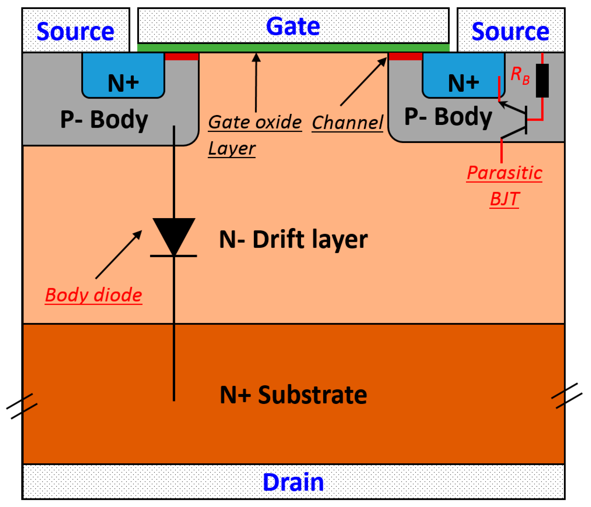
Abstract
:1. Introduction
- (1)
- Wider bandgap (Eg)—approximately 3.23 eV as compared to 1.1 eV in Si;
- (2)
- Higher critical electrical field (EC)—approximately 10 times than in Si;
- (3)
- Higher thermal conductivity (λ) at a given temperature—around 3–5 times that of Si.
2. MOSFET Avalanche Breakdown
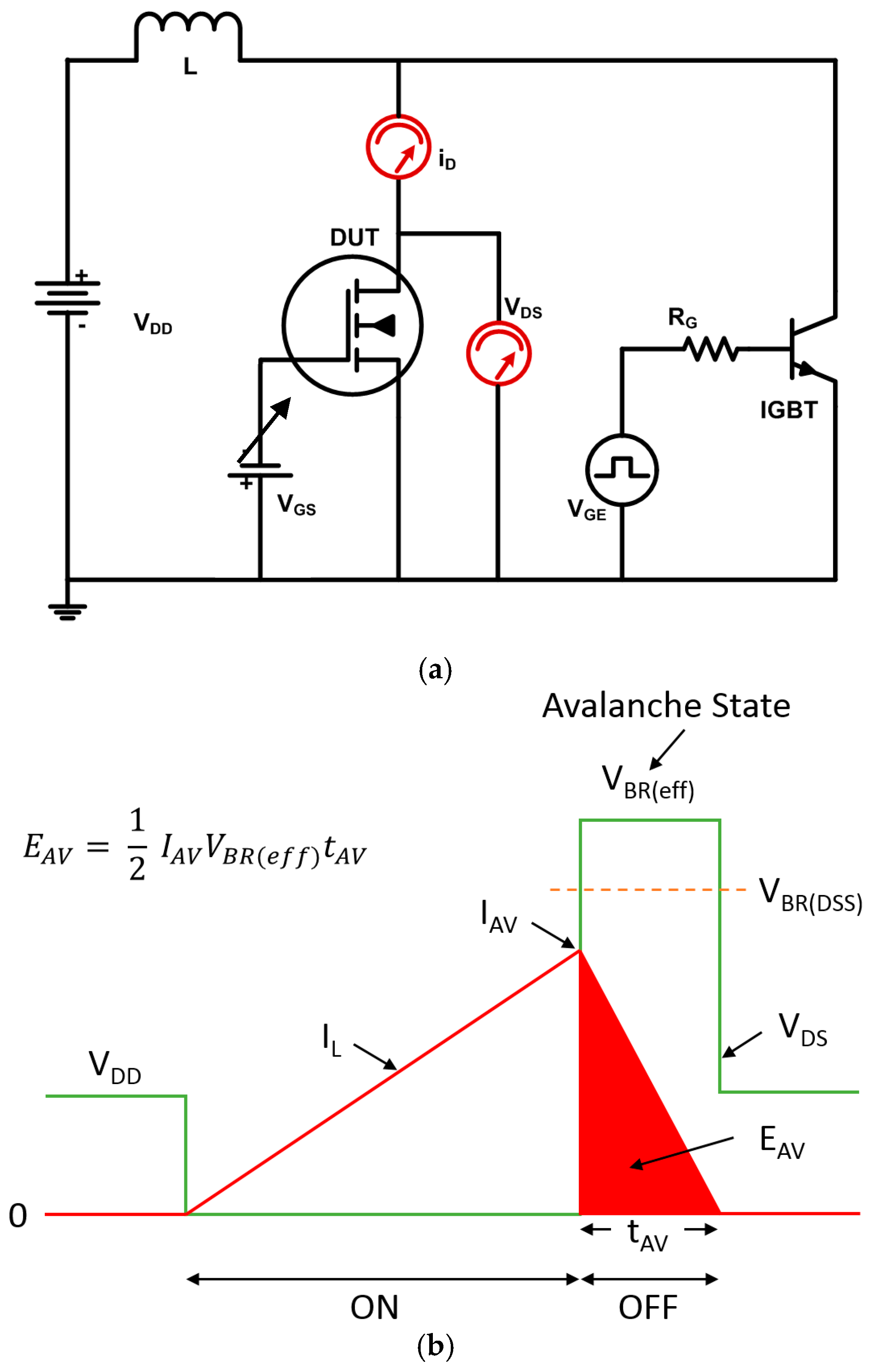
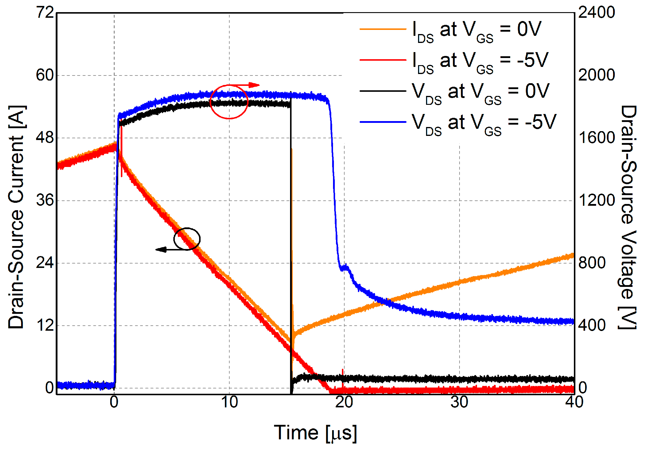
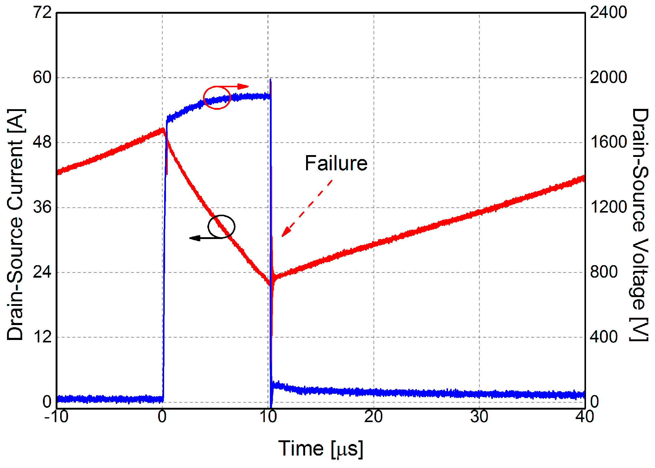
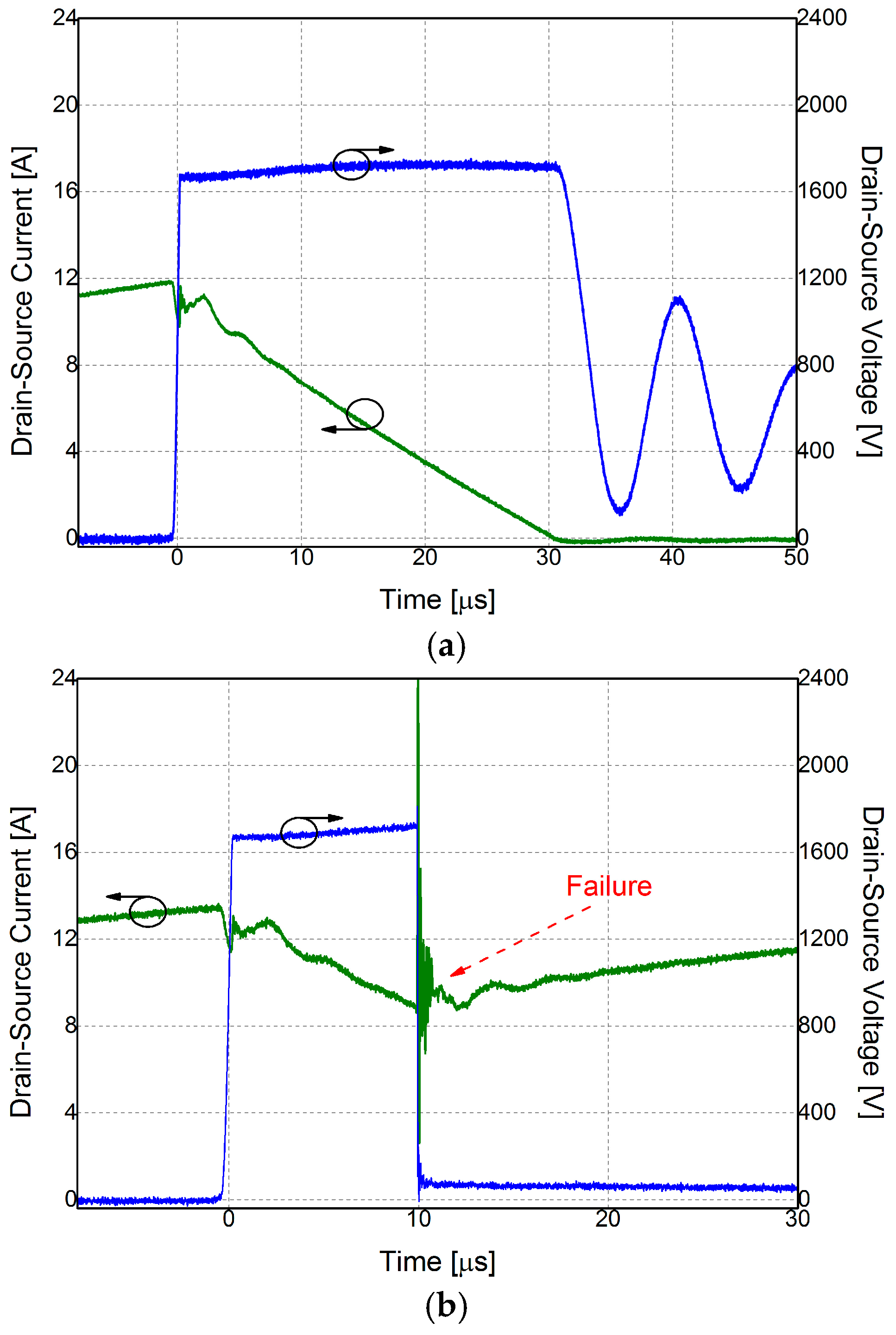
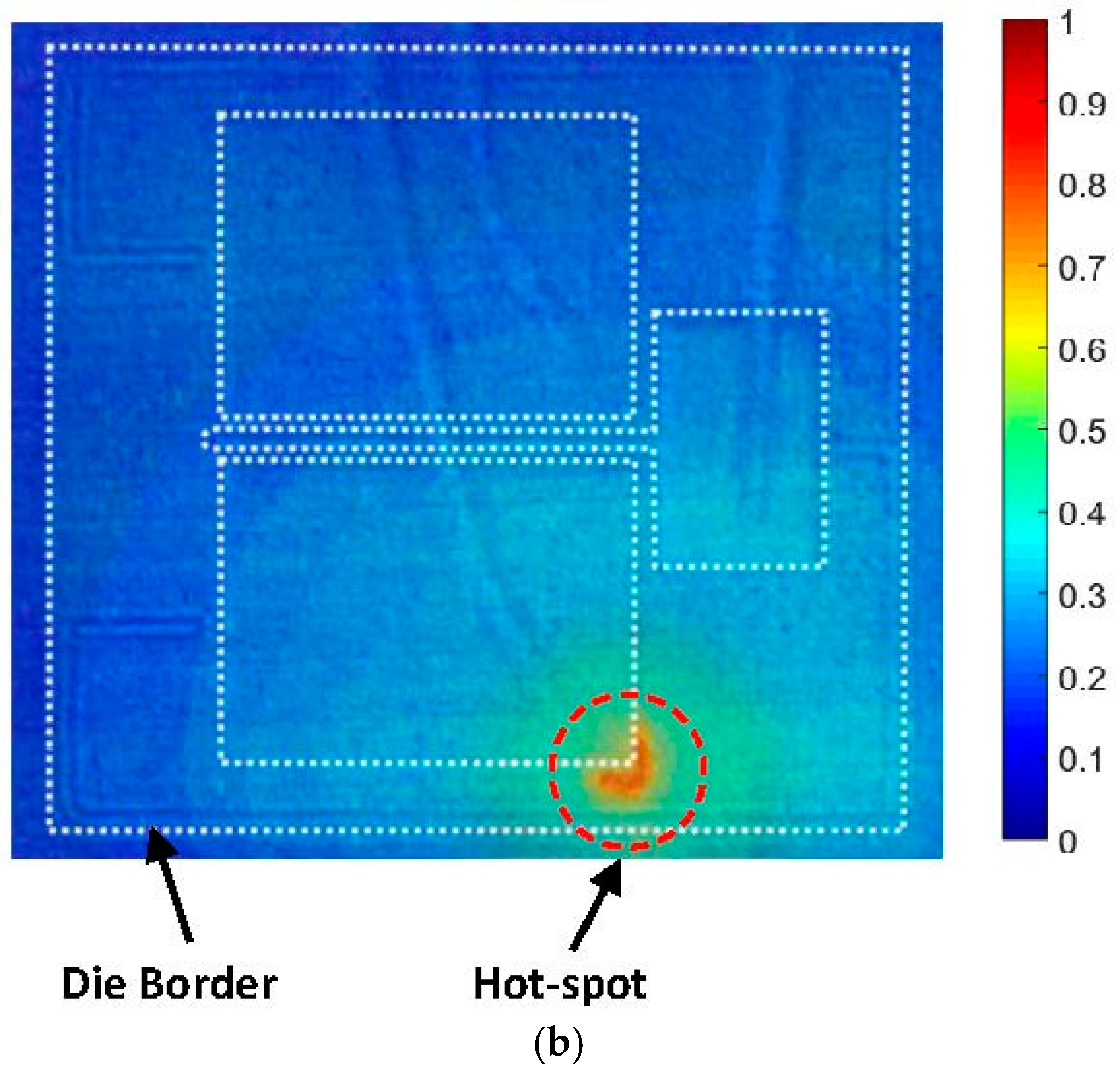
3. Experimental Results
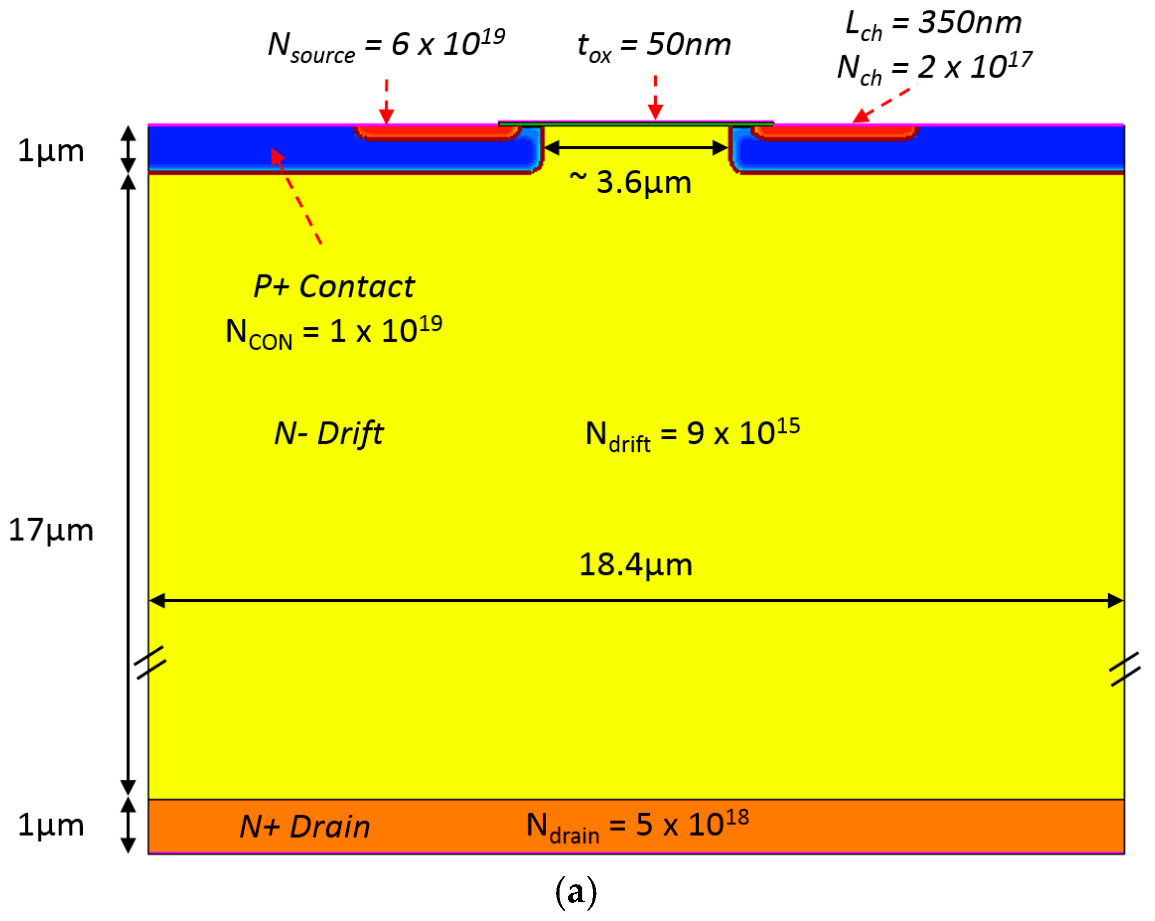
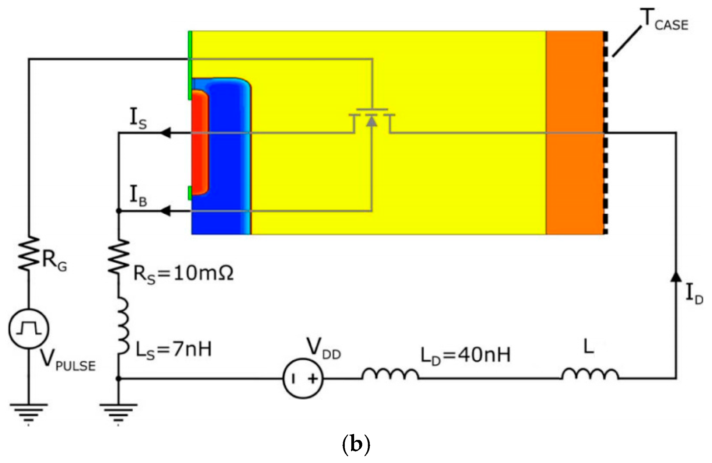
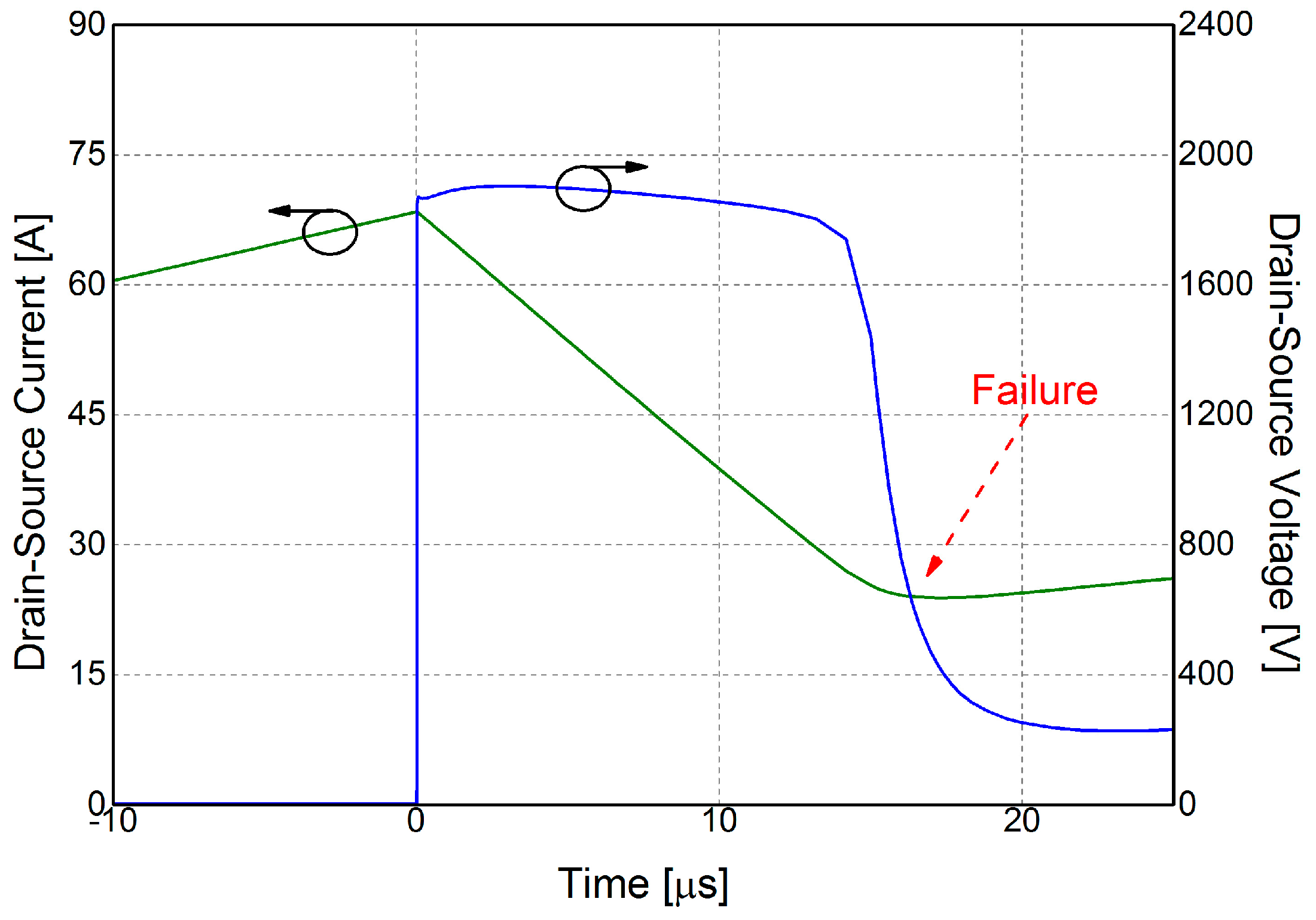
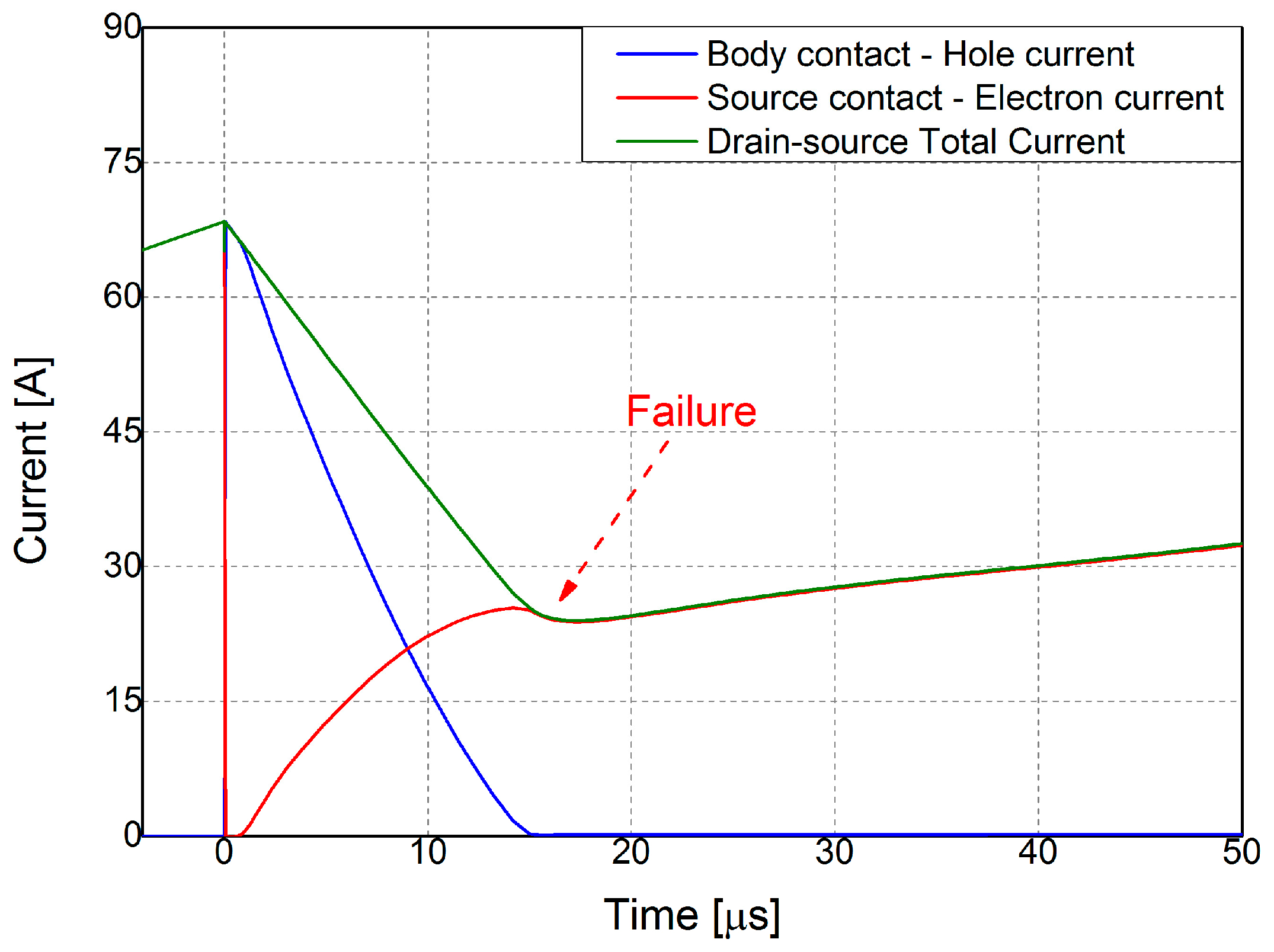
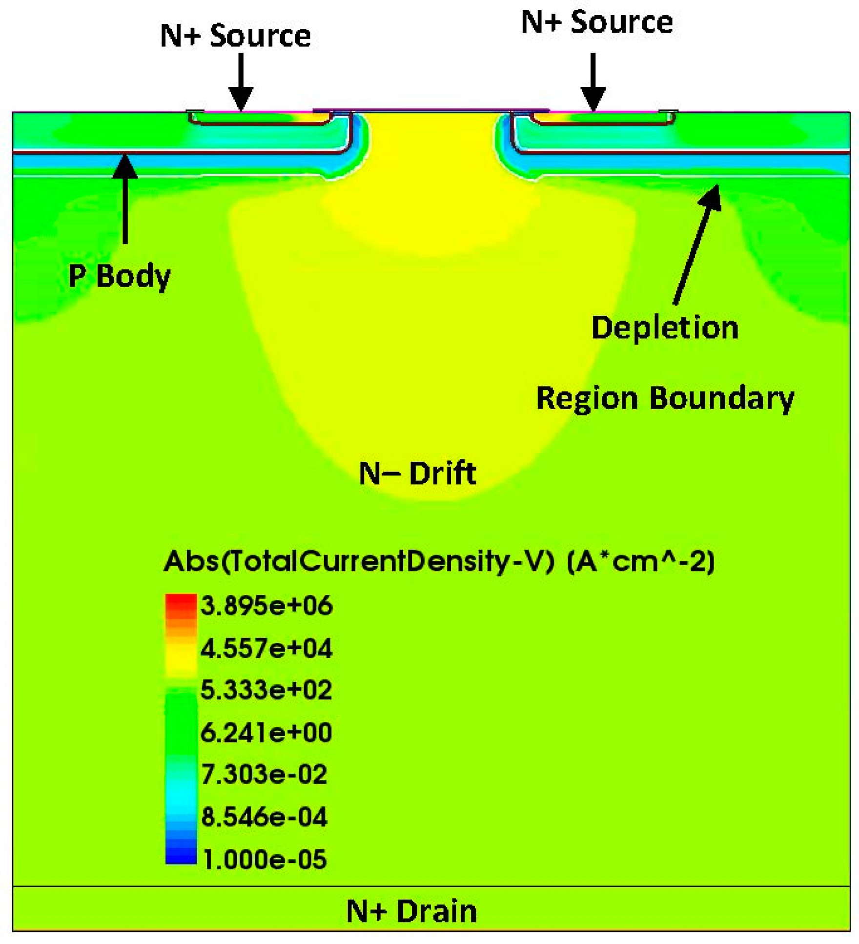
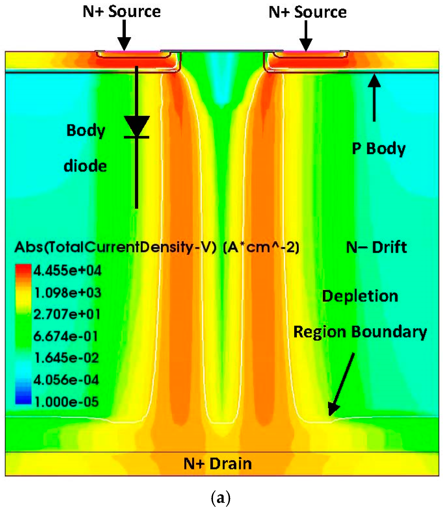
4. TCAD Electro-Thermal Simulations
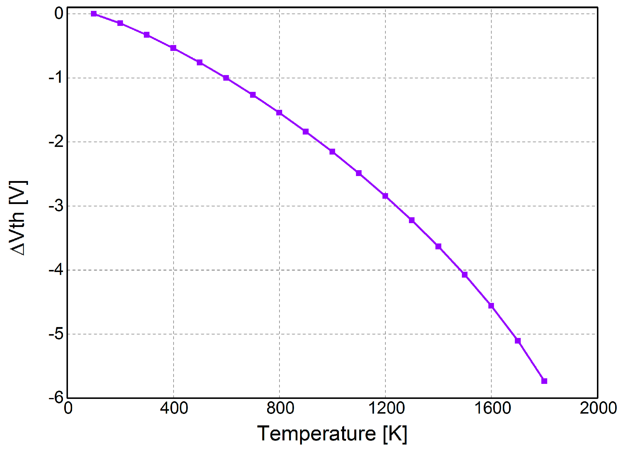
5. Analytical Calculation of Threshold Voltage
- Substrate doping concentration (NA): 3 × 1017 cm−3;
- Gate oxide thickness (tox): 50 nm;
- Oxide charge density (Nox): 1 × 1010 cm−3;
- Oxide permittivity (εSiO2): 3.45 × 10⁻¹¹ F/m;
- Silicon carbide permittivity (εSiC): 8.55 × 10⁻¹¹ F/m;
- Metal work function (): 4.1 eV for aluminum (Al);
- SiC electron affinity (): 3.2 eV.
6. Structural Characterization
7. Conclusions
Author Contributions
Conflicts of Interest
References
- Treu, M.; Rupp, R.; Sölkner, G. Reliability of SiC power devices and its influence on their commercialization—Review, status, and remaining issues. In Proceedings of the 2010 IEEE International Reliability Physics Symposium, Anaheim, CA, USA, 2–6 May 2010; pp. 156–161. [Google Scholar]
- Casady, J.B.; Pala, V.; Lichtenwalner, D.J.; Van Brunt, E.; Wang, G.-Y.; Richmond, J.; Allen, S.T.; Grider, D.; Palmour, J.W. New generation 10 kV SiC power MOSFET and diodes for industrial applications. In Proceedings of the Power Conversion and Intelligent Motion (PCIM) Europe 2015, International Exhibition and Conference for Power Electronics, Intelligent Motion, Renewable Energy and Energy Management, Nuremberg, Germany, 19–20 May 2015; pp. 1–8. [Google Scholar]
- Rabkowski, J.; Peftitsis, D.; Nee, H.P. Silicon carbide power transistors: A new era in power electronics is initiated. IEEE Ind. Electron. Mag. 2012, 6, 17–26. [Google Scholar] [CrossRef]
- Elasser, A.; Chow, T.P. Silicon carbide benefits and advantages for power electronics circuits and systems. Proc. IEEE 2002, 90, 969–986. [Google Scholar] [CrossRef]
- Fayyaz, A.; Yang, L.; Riccio, M.; Castellazzi, A.; Irace, A. Single pulse avalanche robustness and repetitive stress ageing of SiC power MOSFETs. Microelectron. Reliab. 2014, 54, 2185–2190. [Google Scholar] [CrossRef]
- DiMarino, C.; Hull, B. Characterization and prediction of the avalanche performance of 1.2 kV SiC MOSFETs. In Proceedings of the 2015 IEEE 3rd Workshop on Wide Bandgap Power Devices and Applications (WiPDA), Blacksburg, VA, USA, 2–4 November 2015; pp. 263–267. [Google Scholar]
- Fayyaz, A.; Romano, G.; Castellazzi, A.; Irace, A. Robustness investigation of SiC power MOSFETs under negative temperature. In Proceedings of the 2016 18th European Conference on Power Electronics and Applications (EPE’16 ECCE Europe), Karlsruhe, Germany, 5–9 September 2016; pp. 1–8. [Google Scholar]
- Nawaz, M. Evaluation of SiC MOSFET power modules under unclamped inductive switching test environment. Microelectron. Reliab. 2016, 63, 97–103. [Google Scholar] [CrossRef]
- Romano, G.; Fayyaz, A.; Riccio, M.; Maresca, L.; Breglio, G.; Castellazzi, A.; Irace, A. A comprehensive study of short-circuit ruggedness of silicon carbide power MOSFETs. IEEE J. Emerg. Sel. Top. Power Electron. 2016, 4, 978–987. [Google Scholar] [CrossRef]
- Liu, S.; Gu, C.; Wei, J.; Qian, Q.; Sun, W.; Huang, A.Q. Repetitive unclamped-inductive-switching-induced electrical parameters degradations and simulation optimizations for 4H-SiC MOSFETs. IEEE Trans. Electron Devices 2016, 63, 4331–4338. [Google Scholar] [CrossRef]
- Murray, A.F.; McDonald, T.; Davis, H.; Cao, J.; Spring, K. Extremely Rugged MOSFET Technology with Ultra Low RDS (on) Specified for a Broad Range of EAR Conditions. Available online: http://www.irf.com/technical-info/whitepaper/pcim2000.pdf (accessed on 12 January 2017).
- Fischer, K.; Shenai, K. Dynamics of power MOSFET switching under unclamped inductive loading conditions. IEEE Trans. Electron Devices 1996, 43, 1007–1015. [Google Scholar] [CrossRef]
- Losee, P.; Bolotnikov, A.; Yu, L.; Beaupre, R.; Stum, Z.; Kennerly, S.; Dunne, G.; Sui, Y.; Kretchmer, J.; Johnson, A.; et al. 1.2 kV class SiC MOSFETs with improved performance over wide operating temperature. In Proceedings of the 2014 IEEE 26th International Symposium on Power Semiconductor Devices & IC’s (ISPSD), Waikoloa, HI, USA, 15–19 June 2014; pp. 297–300. [Google Scholar]
- Fayyaz, A.; Yang, L.; Castellazzi, A. Transient robustness testing of silicon carbide (SiC) power MOSFETs. In Proceedings of the 2013 15th European Conference on Power Electronics and Applications (EPE), Lille, France, 2–6 September 2013; pp. 1–10. [Google Scholar]
- Baliga, B.J. Silicon Carbide Power Devices; World Scientific: River Edge, NJ, USA, 2012. [Google Scholar]
- C2M0080120D Datasheet; Wolfspeed: Durham, NC, USA, 2015.
- Fu, R.; Grekov, A.; Hudgins, J.; Mantooth, A.; Santi, E. Power SiC DMOSFET model accounting for nonuniform current distribution in JFET region. IEEE Trans. Ind. Appl. 2012, 48, 181–190. [Google Scholar] [CrossRef]
- New Semiconductor Materials: Characteristics and Properties. Available online: http://www.ioffe.ru/SVA/NSM/ (accessed on 12 January 2017).
- Goldberg, Y.; Levinshtein, M.E.; Rumyantsev, S.L. Properties of Advanced Semiconductor Materials GaN, AlN, SiC, BN, SiC, SiGe; John Wiley & Sons, Inc.: New York, NY, USA, 2001; pp. 93–148. [Google Scholar]
- Haberstroh, C.; Helbig, R.; Stein, R.A. Some new features of the photoluminescence of SiC (6H), SiC (4H), and SiC (15R). J. Appl. Phys. 1994, 76, 509. [Google Scholar] [CrossRef]
- Romano, G.; Riccio, M.; De Falco, G.; Maresca, L.; Irace, A.; Breglio, G. An ultrafast IR thermography system for transient temperature detection on electronic devices. In Proceedings of the 2014 30th Annual Semiconductor Thermal Measurement and Management Symposium (SEMI-THERM), San Jose, CA, USA, 9–13 March 2014; pp. 80–84. [Google Scholar]
- Riccio, M.; Pantellini, A.; Irace, A.; Breglio, G.; Nanni, A.; Lanzieri, C. Electro-thermal characterization of AlGaN/GaN HEMT on silicon microstrip technology. Microelectron. Reliab. 2011, 51, 1725–1729. [Google Scholar] [CrossRef]
- Castellazzi, A.; Kartal, V.; Kraus, R.; Seliger, N.; Honsberg-Riedl, M.; Schmitt-Landsiedel, D. Hot-spot meaurements and analysis of electro-thermal effects in low-voltage power-MOSFET’s. Microelectron. Reliab. 2003, 43, 1877–1882. [Google Scholar] [CrossRef]


© 2017 by the authors. Licensee MDPI, Basel, Switzerland. This article is an open access article distributed under the terms and conditions of the Creative Commons Attribution (CC BY) license (http://creativecommons.org/licenses/by/4.0/).
Share and Cite
Fayyaz, A.; Romano, G.; Urresti, J.; Riccio, M.; Castellazzi, A.; Irace, A.; Wright, N. A Comprehensive Study on the Avalanche Breakdown Robustness of Silicon Carbide Power MOSFETs. Energies 2017, 10, 452. https://doi.org/10.3390/en10040452
Fayyaz A, Romano G, Urresti J, Riccio M, Castellazzi A, Irace A, Wright N. A Comprehensive Study on the Avalanche Breakdown Robustness of Silicon Carbide Power MOSFETs. Energies. 2017; 10(4):452. https://doi.org/10.3390/en10040452
Chicago/Turabian StyleFayyaz, Asad, Gianpaolo Romano, Jesus Urresti, Michele Riccio, Alberto Castellazzi, Andrea Irace, and Nick Wright. 2017. "A Comprehensive Study on the Avalanche Breakdown Robustness of Silicon Carbide Power MOSFETs" Energies 10, no. 4: 452. https://doi.org/10.3390/en10040452