A Novel Meander Split Power/Ground Plane Reducing Crosstalk of Traces Crossing Over


1
Department of Electronic Engineering, Sogang University, Seoul 04107, Korea
2
Marine Security and Safety Research Center, Korea Institute of Ocean Science & Technology, Busan 49111, Korea
Electronics 2019, 8(9), 1041; https://doi.org/10.3390/electronics8091041
Submission received: 29 August 2019
/
Revised: 14 September 2019
/
Accepted: 16 September 2019
/
Published: 17 September 2019
(This article belongs to the Special Issue Electromagnetic Interference and Compatibility)
Abstract
:In this paper, a novel meander split power/ground plane is proposed for reducing crosstalk between parallel lines crossing over it. The working mechanism of the meander split scheme is investigated by simulations and measurements. The LC equivalent circuit and transmission line model are developed for modeling interactions between the meander split and the signal lines. The proposed meander structure enhances electromagnetic coupling between split planes. The capacitive coupling across the split ensures signal integrity and magnetic coupling between adjacent finger shaped structures suppresses lateral wave propagation along the split gap, which in turn helps suppress the crosstalk. The effectiveness of the meander split remains valid over very wide frequency ranges (up to 9 GHz). Experimental results show that the proposed structure improves the signal quality and reduces the near/far end crosstalk over 30 dB and 50% in the frequency domain and time domain, respectively.
1. Introduction
In high-speed electronic systems, the power and ground planes play important roles as a reservoir in supplying power to components and as a voltage reference on printed circuit boards. To accommodate the rapidly switching components and their demand for current, an ideal power supply should have very low impedances, which necessitates the use of power and ground planes. However, the plane pair effectively forms a parallel plate waveguide, which can hold persistent ringing noises generated by routed traces and vias to and from components on the circuit board. To reduce the noise coupling due to power planes and provide different power supply voltages, slotted or split plane types are frequently used for the integrated circuits or modules [1,2,3] occupying the same printed circuit boards (PCBs) [4,5]. However, power/ground partitioning generates undesired electromagnetic effects such as signal integrity degradation, electromagnetic interference (EMI) and crosstalk when signal lines cross over the split gaps [6,7,8,9,10]. When two parallel line traces cross over slots or splits in the planes, the crosstalk level between the traces becomes high even for large clearances [11].
Commonly used methods to reduce crosstalk are placing via fences [12], guard traces [13], serpentine guard traces [14], stubs [15], or resonators [16] between the two signal lines. Recently, a method of coating signal lines with graphene-paraffin has also been studied [17]. In most of the approaches, efforts are made to decrease the crosstalk levels by inserting additional structures between the conventional transmission lines. Defective microstrip line structures [18] and stub-alternated microstrip lines [19] have been used for the reduction of crosstalk. With these methods, the complexity of the PCBs is increased due to the additional structures.
Attaching stitching capacitors [11,20] or inter-digital capacitors [21] between the split gap under the signal lines reduces the crosstalk and provides return current paths at high frequency while maintaining distinct dc levels of each region. However, this requires additional processes or costs and sometimes it is hard to make room for the stitching capacitor right below the signal trace. Furthermore, the effectiveness of these approaches is limited in that the equivalent series inductance of the capacitors dominates the impedance of a decoupling capacitor at higher frequencies [22]. Another commonly used approach is the addition a low-Q inductor or a thin inductive trace or stubs [23,24] on split power planes. However, this remedy cannot isolate wideband switching noises generated by each functional block on the same PCB, and cannot accommodate different power supply voltages.
Recently, various shapes of defective ground structures (DGS) such as the “U”, “V”, “H”, rectangular, square, circular, ring and dumbbell shape [25,26,27,28] have been investigated to design the wideband filter without adding any complexity to the original structure. Some complex shapes have also been studied, which include meander lines [29]. All of these studies focus on the design of the filter using DGS, and it is necessary to study DGS for their crosstalk reduction effect. Recently, several studies [30,31] have investigated the reduction of crosstalk using rectangular or dumbbell DGS shapes on the ground plane, finding that the reduction effectiveness is 20 dB over a frequency range of 5 GHz.
In this paper, a novel meandered DGS embedded on a split plane is proposed and investigated from the view point of signal transmission and crosstalk reduction. The equivalent circuit model based on slot-coupled cavity equivalent circuit and transmission line theory is presented to describe the behavior of the meandered DGS split gap. The meandered structure enhances capacitive coupling across the split planes, which helps signal transmission of the line traces over a split gap. The structure suppresses lateral wave propagation along the slot-line formed by the split gap by the destructive coupling of the magnetic fields of meandering currents on the adjacent slot line sections. In other words, lateral waves excited along the split gap become evanescent, which helps the return current on the power/ground plane be localized. The crosstalk reduction effectiveness of the split plane with meandered DGS holds 30 dB over a wide frequency range up to 9 GHz, and the crosstalk levels are reduced to over 50% of a simple straight split plane such as a rectangular or dumbbell one [30,31], which is verified by measurements.
2. The Meander DGS on Split Power/Ground Plane
2.1. Advantage and Application of the Meander DGS
In general, the shape, size, and periodicity of the DGS affects the frequency characteristics. A periodic DGS can design well-defined stopbands and passbands and achieve the performance such as high-order filters. DGS can be used in many applications in microwave printed circuits such as filters, amplifiers, oscillators, directional couplers, antennas, and multiplayer stack-up PCBs.
The DGS disturbs the current distribution of the ground plane and changes the characteristics of a transmission line crossing over the DGS [32]. The main disadvantage of the DGS is that they break the return current path and cause spurious radiations in the circuits. The DGS will change the impedance of the ground plane, and lead to spurious radiations. However, our proposed meander DGS has the advantage of providing the return current path by enhancing the coupling between adjacent meander lines. Thus, it can be applied as an excellent method to solve EMI problems such as signal integrity, radiation, and crosstalk.
2.2. Design Methodolgy of the Meander DGS
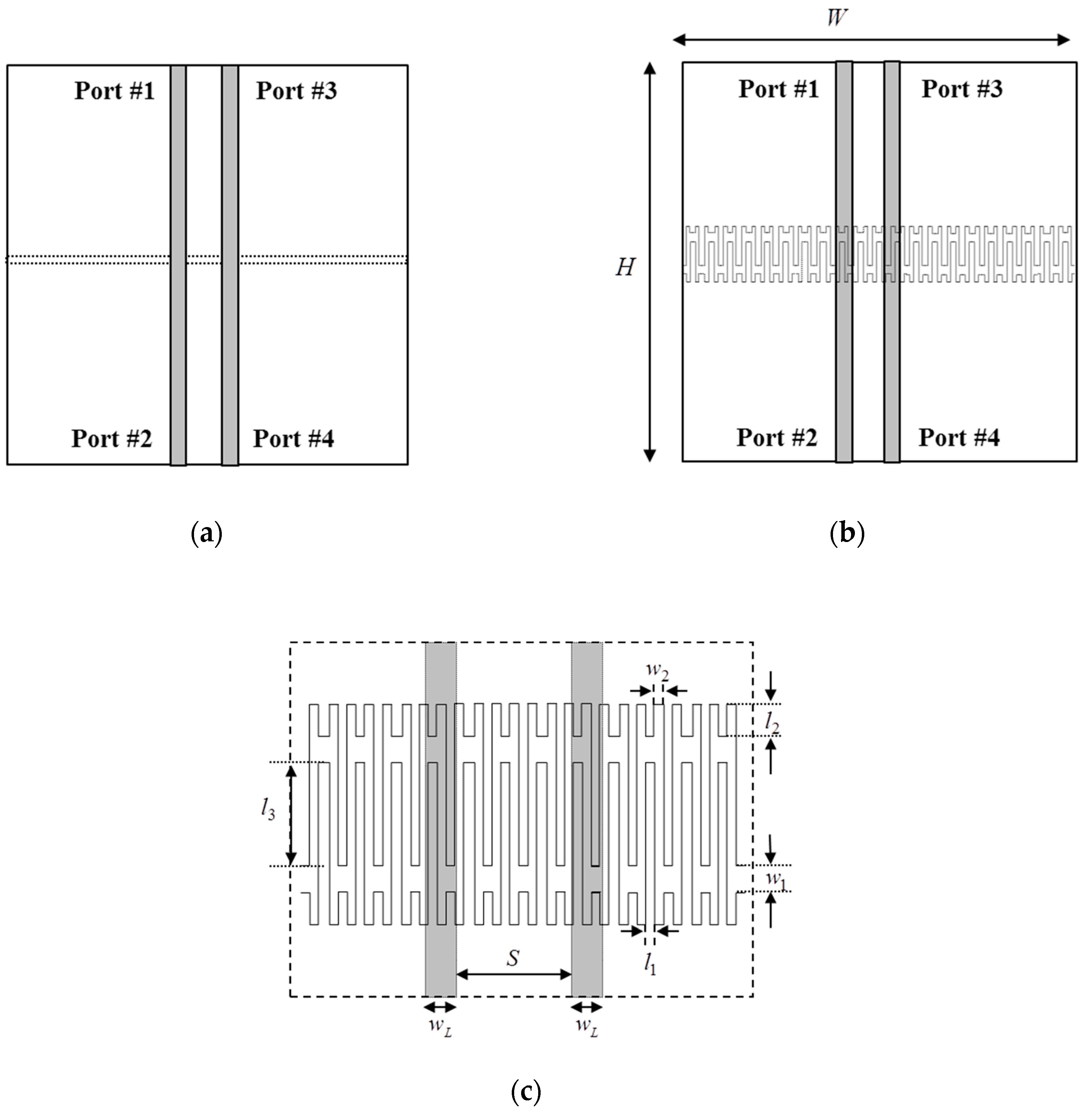
The meander DGS-like asymmetric inter-digital finger in Figure 1c was used in the split ground plane and optimized for the desired frequency of operation. Due to the structure of the meander split on the ground plane, the vertical length ltot and width w1, w2 of the meander split dimension were selected according to the design rule. Within the given criteria (ltot = 2 × w1 + 2 × l2 + l3), the vertical length l3 and width w2 of meander split gap contribute to the mutual inductance and capacitive coupling between the meander gaps, respectively, in Figure 1c. The design parameters related to this electromagnetic coupling are independent of the position of the signal line wL. That is, the wL does not necessarily have to be located right above the center of l1 or w2.
The main design method was to select the vertical length l3 of the meander gap associated with the magnetic coupling and width w2 of the meander gap associated with the capacitive coupling effect for defining the stopband and passband frequency characteristics. The equivalent circuit of the meander DGS and associated parameters were extracted by the LC equivalent circuit model and transmission line model. The periodic placement (N) of the meander DGS enhances the frequency characteristics of the equivalent circuit and improves the crosstalk reduction effect on broadband frequencies.
Figure 1a,b shows two PCBs containing parallel line traces (W = 100 mm, H = 100 mm, S = 10 mm, wL = 1.69 mm) on one side. On the bottom sides of the boards, a simple straight split ground plane, like a rectangular DGS [30,31], and a proposed meandered DGS (w2 = 0.2 mm, l1 = 0.25 mm, w1 = 2 mm, l3 = 20 mm, l2 = 2 mm) embedded split ground plane are formed, respectively. The dielectric material used for the PCBs is FR4 whose relative permittivity is 4.2, and the thickness of the boards is 1.0 mm. The width of the split gaps of the two boards is 2 mm. There are a total of 110 (N) meandering cells in the split in Figure 1c, which are not drawn to real scale. The characteristic impedances of the signal traces above the solid ground plane are set to be 50 Ω to eliminate reflections from the coaxial cables, which connect the board to a network analyzer.
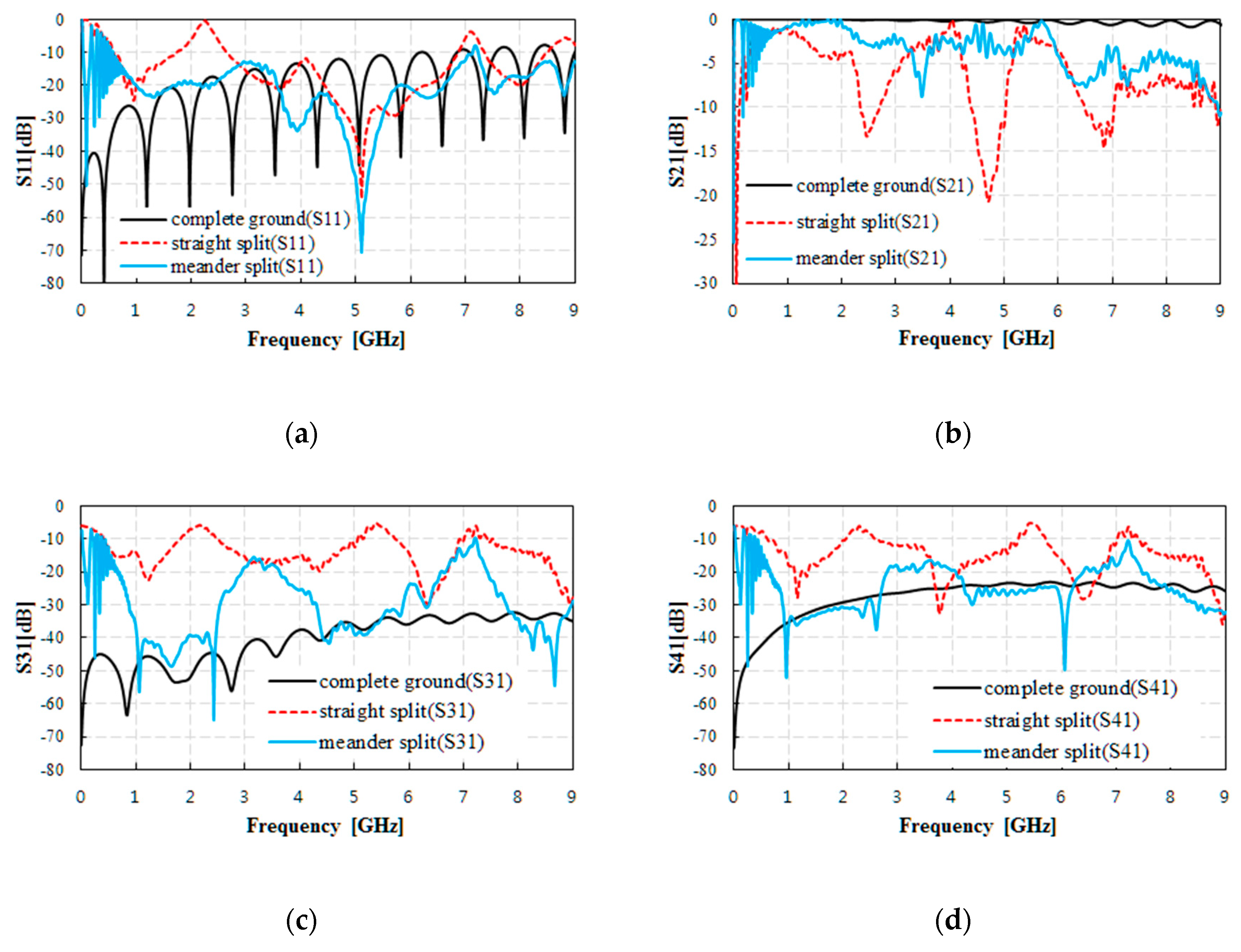
We measured the scattering parameters of the two samples with a complete homogeneous ground plane in Figure 2. As shown in the figure, the reflections occur due to the split gaps, and the scattering parameters show resonant behavior. Compared with the complete homogeneous ground plane, the two split ground planes degrade the signal integrity and increase crosstalk. However, the meander split improves the signal integrity and decreases 30 dB of crosstalk up to 9 GHz more than the straight split ground plane, like a rectangular DGS [30,31]. This difference comes from the enhanced coupling due to the meander structure on the split plane.
2.3. Equivalent Circuit of the Meander DGS Split Model
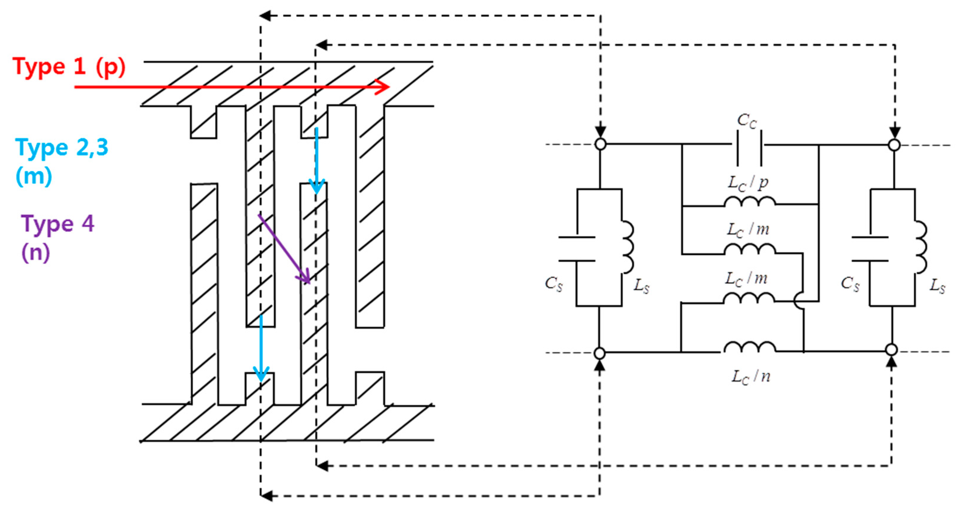
The DGS slot can be modeled in parallel with a capacitor and inductor [32]. Based on the equivalent slot circuit, the LC equivalent circuit of the bottom layer where the ground is a meander gap can be derived in Figure 3. In terms of return current path on the bottom layer, the capacitive and mutual inductance effects exit between the different meanders. The return current paths by the capacitive and mutual inductance effects are represented by the Type 1 (p), Type 2, 3 (m) and Type 4 (n), respectively. The p is the fraction of the return current not involved in the coupling (Type 1), m is the fraction involved in coupling one way only (Type 2 and 3) and n is the fraction involved in coupling one way only (Type 4). The design parameters such as coupling fractions, and the L and C values of the meander structure in Figure 3 were extracted based on the slot-coupled cavity equivalent circuit [33] to define the passband and stopband frequency characteristics.
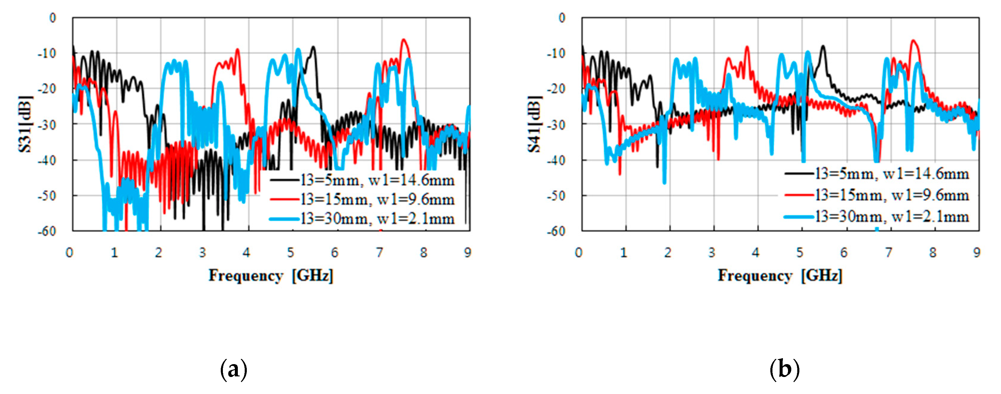
Alternatively, this enhanced coupling phenomenon can be explained using slot line modes excited in the split. Based on the previous analysis and the scheme of the meander structure, the transmission line equivalent circuit model of the meander split gap can be derived in Figure 4. The meander gap away from the signal line is modeled simply by a series of periodic transmission lines with alternately varying characteristic impedances Z1, Z2, Z3, effective dielectric constants εe1, εe2, εe3 and mutual inductances Lm. To observe the vertical length l3 and width w1 of the split gap affecting the crosstalk reduction, we performed a parameter sweep using CST Microwave studio. Due to the structure of the meander split on the ground plane, the vertical length ltot of the meander split cannot be infinitely long. Within the given criteria (ltot = 2 × w1 + 2 × l2 + l3), the vertical length l3 of the meander split gap contributes to the mutual inductance. The width w1 of the meander split gap contributes to the capacitive coupling. We calculated the characteristic impedances and the effective dielectric constants of the slot line as l3 and w1 changes (Table 1) by using the conformal mapping technique [34]. By varying the split gap widths (w1) and length (l3), the frequency characteristics are designed for passband and stopband of the crosstalk at least (Figure 5).
Based on the equivalent circuit of the meander gap, the crosstalk equivalent circuit of Figure 6 can be derived for the meander split on the ground plane. The split gap can be modeled by a slot line with a transformer, which is excited by the signal line above [11]. If the spatial period of the meander structure is small enough, the signal line crosses over the split gap in a number of points, which can be modeled by transformers. It shows that if a signal line crosses over the meander split gap on the ground plane, it excites a transverse electromagnetic (TEM) mode in the mender split gap, which has a structure similar to the slot lines. The excited modes propagate in either direction and are scattered at the corners of the meander line, which impede the propagating modes. The split gap right under the signal line can be regarded as a coupled line structure, of which coupling strength can be changed by varying the longitudinal length dimension of the split.
3. Results
3.1. Simulation Results of the Equivalent Circuit
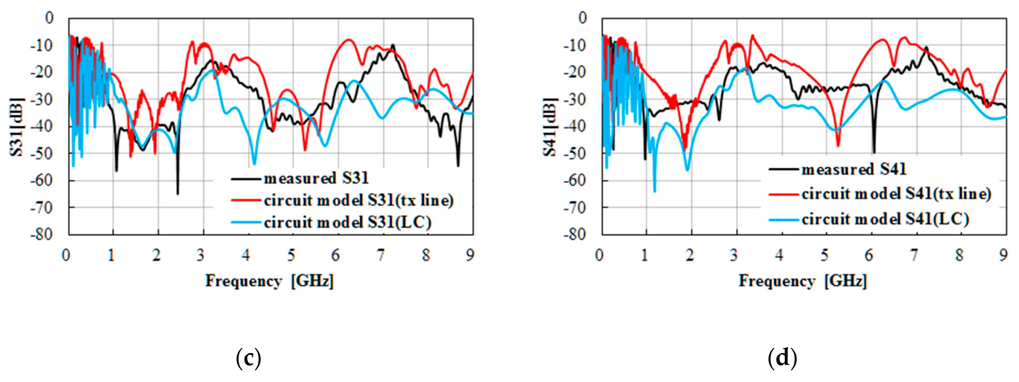
Figure 7 shows the effectiveness of the equivalent circuit of Figure 4 and Figure 5. The crosstalk behaviors of the circuit model simulated using Agilent ADS and measurement show good overall agreement about the peak and zero. At low frequencies below about 3 GHz, the LC equivalent circuit model of Figure 4 was closer to the measured result than the transmission line equivalent model of Figure 5. At high frequencies, the transmission line model was close to the measured result. The mutual inductance effect is proportional to the vertical length of the meander split and their relationship is calculated by the linear interpolation from the simulation and measured result. The crosstalk simulation result of the circuit model is slightly overestimated compared to the measured result because of the interpolation residual error of the mutual inductance value.
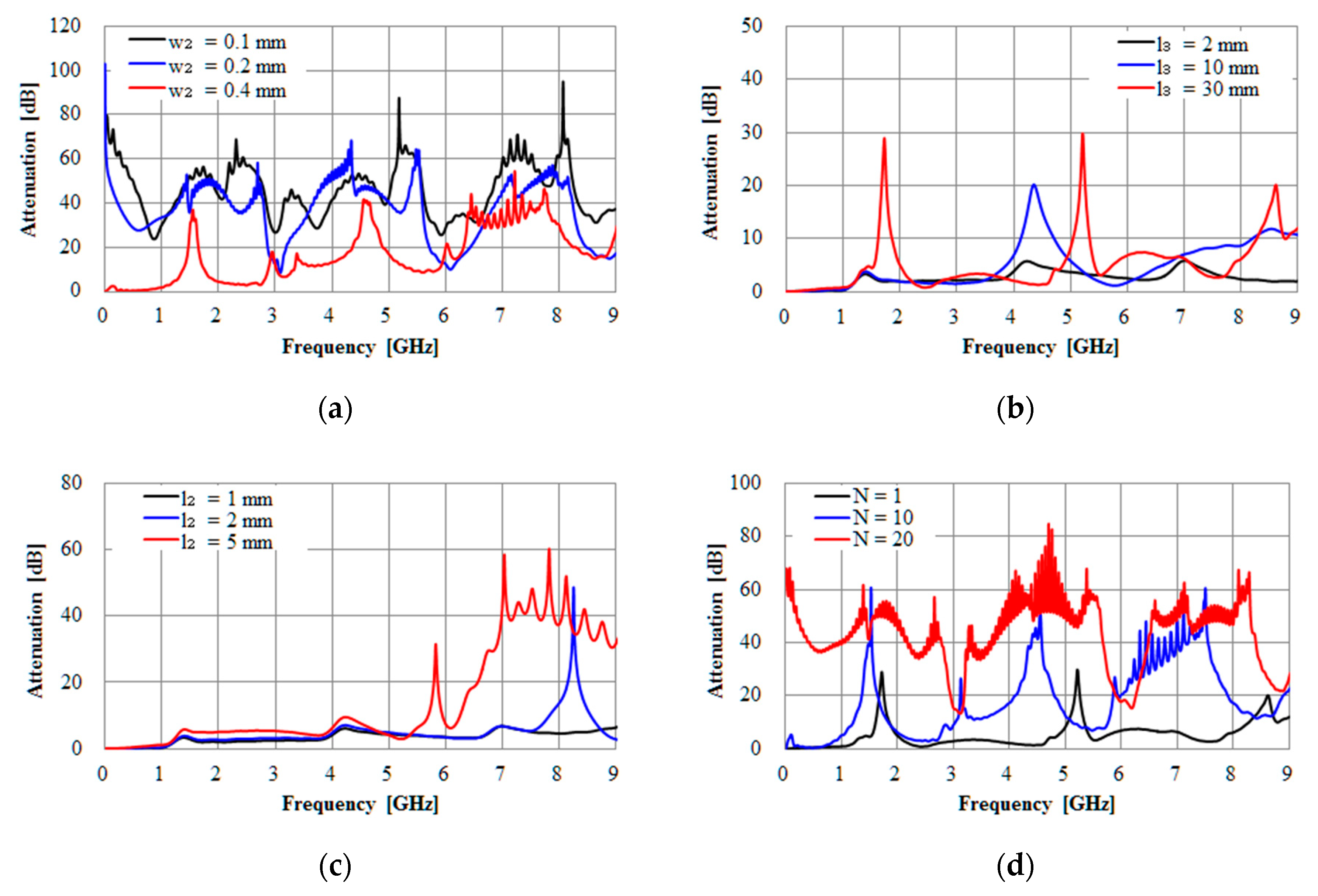
3.2. Reduction of Crosstalk According to the Vertical Length and Width of the Meander Split Gap
The effect of reducing the crosstalk is proportional to the vertical length l3 and l2 and inversely proportional to the split gap width w2. We showed the effectiveness of those design parameters using CST Microwave studio. We set the discrete ports at the start and end point of the transmission line equivalent circuit of the meander slot line in Figure 4. Figure 8 shows the more narrowly split gap width w2 that increases capacitive coupling and the longer length of l3 and l2 that causes destructive magnetic coupling with a shortened circuit line and less lateral wave propagation. The shortened circuit transmission lines (l2) have reactance that impedes lateral wave propagation (Figure 8c). By increasing the number of cells (N) of the meander slot line, as well as varying the meander line length and split gap widths, the excited slot line mode is suppressed or attenuated (Figure 8d).
Therefore, the reduction of crosstalk at the lower and upper frequency has improved, which is desirable for digital signal transmission. The meander split gaps away from the signal line attenuate the scattered waves entering the slot line. Thanks to the evanescent mode, the periodic resonant behavior disappears, which effectively helps the signal transmission and reduces the crosstalk.
These differences come from the enhanced electromagnetic coupling between neighboring slot line sections of split planes. The meander split structure increases capacitive coupling due to the narrow split gap width, and increased length of the interaction causes destructive magnetic coupling due to the oppositely directed currents on nearby slot line sections. The capacitive coupling decreases impedance across the split gap, and the magnetic coupling increases impedances along the split. With the increased impedance, the return current cannot spread perpendicularly to the signal line. The effect causes the return current to be formed near the signal line, which helps the return current flow across the split gap without detouring. The localized return current improves signal integrity of the line traces formed over the split more effectively than the straight split.
3.3. Time Domain Crosstalk Simulation Results
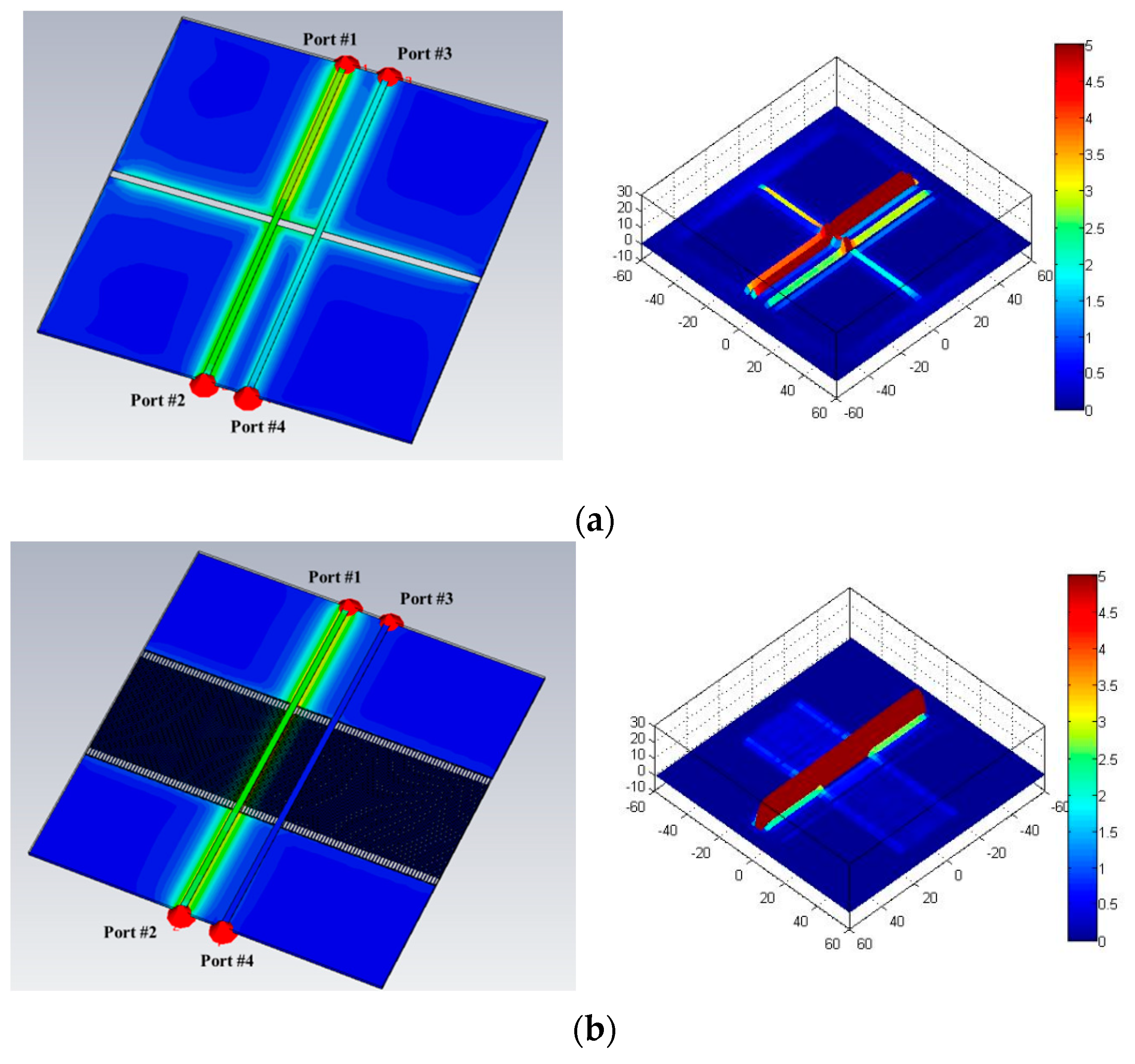
The crosstalk can be explained by the current distribution on the printed circuit board. We used CST Microwave studio to obtain the current distributions of the two types of circuit boards. Figure 9 shows the surface current distribution at 2 GHz. In the case of the straight split gap, currents flow along the edge of the split and reflect at the open ends of the PCB, which enhances coupling between the two parallel signal lines and causes crosstalk. For the meander split gap, most currents cross over the meander split gap near the signal line, which shows the effectiveness of the proposed structure. Following the meander DGS split gap, the increased impedance caused by currents with alternating directions causes the crosstalk signal to be reduced effectively.
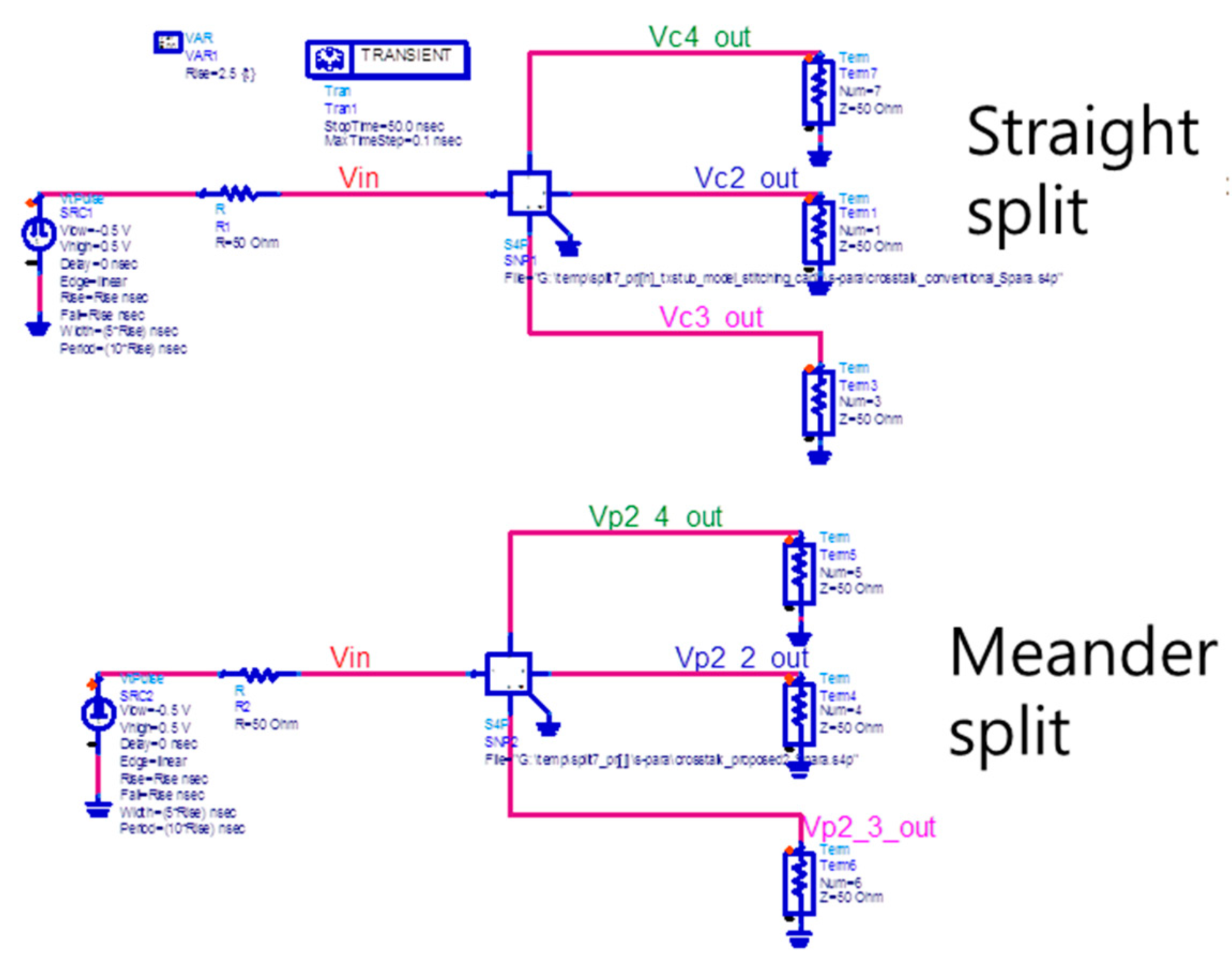
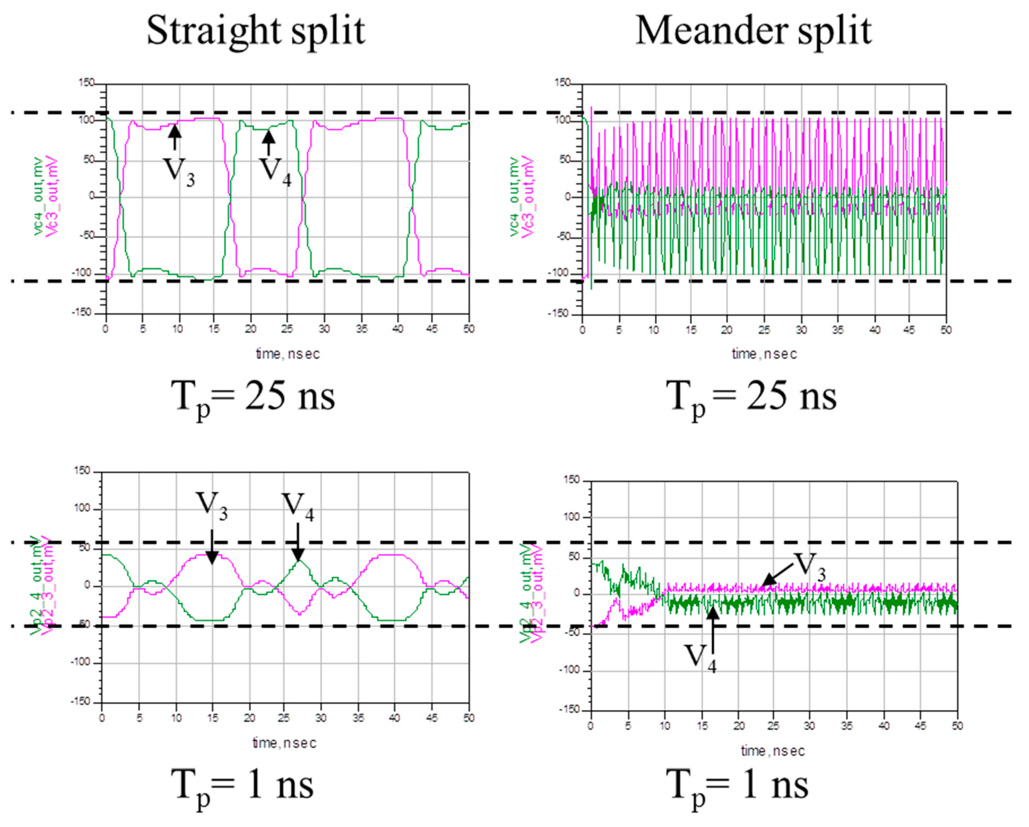
The crosstalk behavior of the transmission line equivalent circuit model for the meander DGS split is simulated in the time domain by using Agilent ADS in Figure 10. We excited a source pulse voltage 1Vp-p with 50 ohm and checked the voltage of V3 (port #3) and V4 (port #4). Figure 11 shows when the fast pulse signal is excited, the proposed meander DGS split decreases the crosstalk voltage at port #3 and #4 over 50% more than the straight split.
3.4. Time Domain Crosstalk Measurement Results
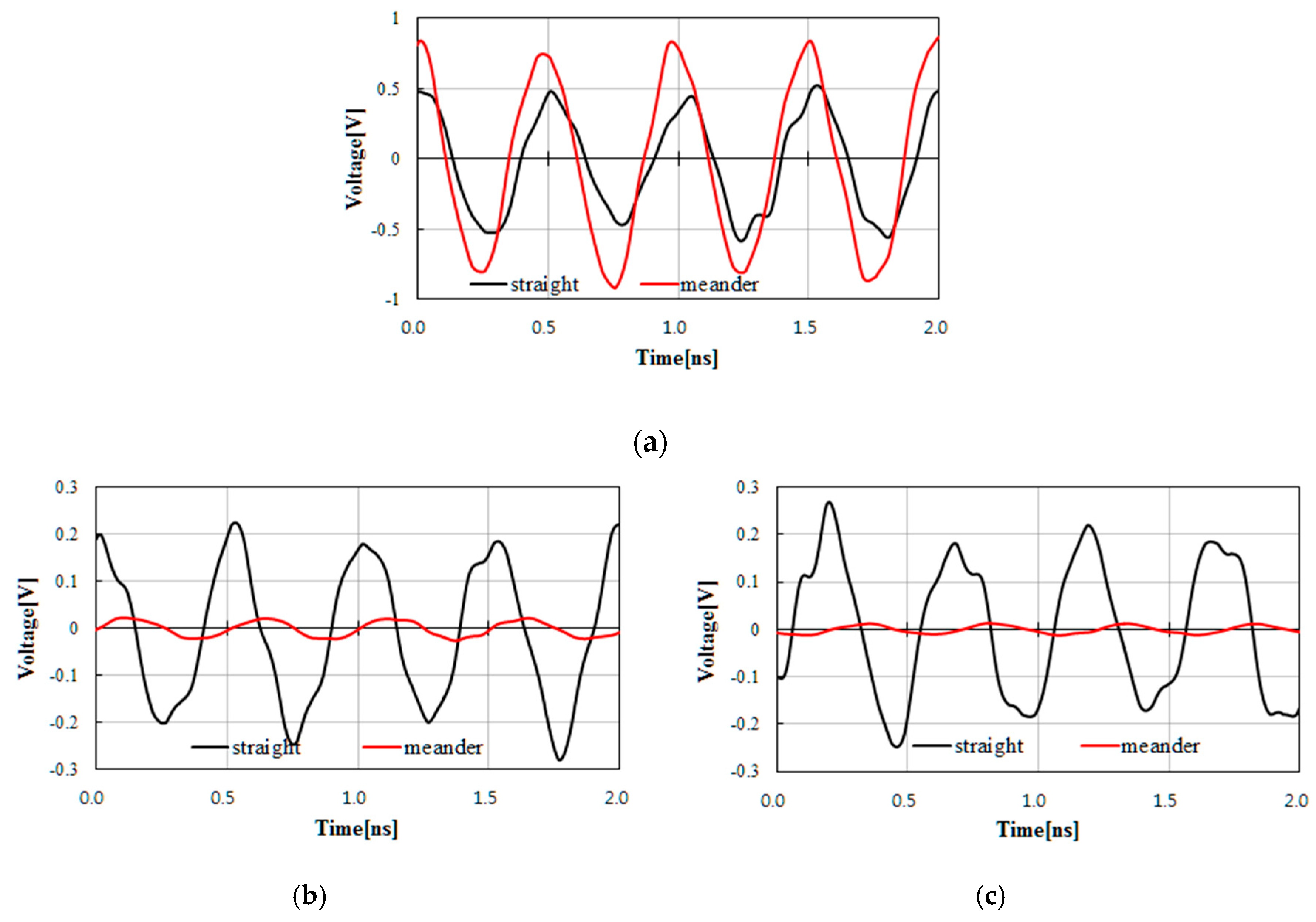
In order to demonstrate the effectiveness of the proposed split method, the crosstalk behavior of the straight and proposed split was observed experimentally in the time domain. The measurements were made by a digital oscilloscope (Tektronix TDS 6604B) and a RF signal generator (Rohde&Schwarz SML 03). The characteristic of the input RF signal is as follows. The frequency is 2 GHz, amplitude is 0.8 V. The input port #1 is fed into the RF signal generator in Figure 1. All the other ends of the lines such as port #2 (transmission), port #3 (near-end crosstalk) and port #4 (far-end crosstalk) are fed into the digital oscilloscope. Figure 12 shows the peak-to-peak voltage of the transmission signal of the meander split is larger than the straight split and it reduces near/far end crosstalk by over 50%. This behavior demonstrates that the proposed meander split power/ground plane can effectively eliminate the reflection and crosstalk due to a split gap and increase transmission bandwidth in the time domain.
4. Conclusions
A novel meander DGS is proposed to improve the transmission bandwidth and reduce the crosstalk of the two parallel microstrip lines over split power/ground planes. It employs a meander split to enhance electromagnetic coupling and suppress propagation of lateral waves to make signal return current flow across the split formed in the power/ground plane along the signal line in proximity, which helps reduce the crosstalk effectively. We have presented a design method for the main parameters l3 and w2 of the meander DGS that enhanced electromagnetic coupling and reduced the crosstalk. We developed the LC equivalent circuit and transmission line equivalent circuit model for analyzing the crosstalk. The validity of the equivalent circuit model was verified by comparison with measurement and simulation results and it shows overall good agreement with slight overestimation due to the mutual inductance interpolation error. Experimental results show that the proposed meander DGS improves signal quality and reduces near/far end crosstalk over 30 dB up to 9 GHz and 50% in the frequency domain and time domain, respectively.
Author Contributions
Conceptualization, methodology, investigation, writing-original draft preparation, writing-review and editing, J.-H.L.
Funding
This research was funded by Korea Institute of Ocean Science & Technology, grant number PE99741.
Acknowledgments
This research was part of the project titled “Development of maritime defense and security technology [PE99741]” funded by Korea Institute of Ocean Science & Technology in 2019.
Conflicts of Interest
The author declares no conflict of interest.
References
- Fan, J.; Ren, Y.; Chen, J.; Hockanson, D.M.; Shi, H.; Drewniak, J.L.; Hubing, T.H.; Van Doren, T.P.; DuBroff, R.E. RF isolation using power islands in DC power bus design. In Proceedings of the 1999 IEEE International Symposium on Electromagnetic Compatability. Symposium Record (Cat. No. 99CH36261), Seattle, WA, USA, 2–6 August 1999; pp. 838–843. [Google Scholar]
- Miller, J.R. The impact of split power planes on package performance. In Proceedings of the 2001 Proceedings. 51st Electronic Components and Technology Conference (Cat. No. 01CH37220), Orlando, FL, USA, 29 May–1 June 2001; pp. 1117–1121. [Google Scholar]
- Liaw, H.-J.; Merkelo, H. Signal integrity issues at split ground and power planes. In Proceedings of the 1996 Proceedings 46th Electronic Components and Technology Conference, Orlando, FL, USA, 28–31 May 1996; pp. 752–755. [Google Scholar]
- Shim, H.-Y.; Kim, J.; Yook, J.-G. Modeling of ESD and EMI problems in split multi-layer power distribution network. In Proceedings of the 2003 IEEE Symposium on Electromagnetic Compatibility. Symposium Record (Cat. No. 03CH37446), Boston, MA, USA, 18–22 August 2003; pp. 48–51. [Google Scholar]
- Cui, W.; Fan, J.; Ren, Y.; Shi, H.; Drewniak, J.; Dubroff, R. DC power-bus noise isolation with power-plane segmentation. IEEE Trans. Electromagn. Compat. 2003, 45, 436–443. [Google Scholar] [CrossRef]
- Johnson, H.W.; Graham, M. High-Speed Digital Design: A Handbook of Black Magic; Prentice Hall: Upper Saddle River, NJ, USA, 1993. [Google Scholar]
- Shuppert, B. Microstrip/slotline transitions: Modeling and experimental investigation. IEEE Trans. Microwave Theory Tech. 1988, 36, 1272–1282. [Google Scholar] [CrossRef]
- Duan, D.-W.; Rubin, B.J.; Magerlein, J. Distributed effects of a gap in power/ground planes. In Proceedings of the IEEE 8th Topical Meeting on Electrical Performance of Electronic Packaging (Cat. No. 99TH8412), San Diego, CA, USA, 25–27 October 1999; pp. 207–210. [Google Scholar]
- Schuster, C.; Fichtner, W. Parasitic modes on printed circuit boards and their effects on EMC and signal integrity. IEEE Trans. Electromagn. Compat. 2001, 43, 416–425. [Google Scholar] [CrossRef]
- Moran, T.; Virga, K.; Aguirre, G.; Prince, J. Methods to reduce radiation from split ground planes in RF and mixed signal packaging structures. IEEE Trans. Adv. Packag. 2002, 25, 409–416. [Google Scholar] [CrossRef]
- Xiao, F.; Nakada, Y.; Murano, K.; Kami, Y. Crosstalk analysis model for traces crossing split ground plane and its reduction by stitching capacitor. Electron. Commun. Jpn. (Part II: Electron.) 2007, 90, 26–34. [Google Scholar] [CrossRef]
- Suntives, A.; Khajooeizadeh, A.; Abhari, R. Using via fences for crosstalk reduction in PCB circuits. In Proceedings of the 2006 IEEE International Symposium on Electromagnetic Compatibility, Portland, OR, USA, 14–18 August 2006; pp. 34–37. [Google Scholar]
- Mbairi, F.D.; Siebert, W.P.; Hesselbom, H. On The Problem of Using Guard Traces for High Frequency Differential Lines Crosstalk Reduction. IEEE Trans. Compo. Packag. Technol. 2007, 30, 67–74. [Google Scholar] [CrossRef]
- Huang, W.-T.; Lu, C.-H.; Lin, D.-B. SUPPRESSION OF CROSSTALK USING SERPENTINE GUARD TRACE VIAS. Prog. Electromagn. Res. 2010, 109, 37–61. [Google Scholar] [CrossRef] [Green Version]
- Koo, S.-K.; Lee, H.; Park, Y.B. Crosstalk Reduction Effect of Asymmetric Stub Loaded Lines. J. Electromagn. Waves Appl. 2011, 25, 1156–1167. [Google Scholar] [CrossRef]
- Chu, S.T.; Little, B.; Pan, W.; Kaneko, T.; Kokubun, Y. Cascaded microring resonators for crosstalk reduction and spectrum cleanup in add-drop filters. IEEE Photonics Technol. Lett. 1999, 11, 1423–1425. [Google Scholar]
- Cai, Q.-M.; Yu, X.-B.; Zhang, L.; Zhu, L.; Zhang, C.; Ren, Y.; Fan, J. Far-End Crosstalk Mitigation in DDR5 Using Graphene-Paraffin Material Coated Signal Lines with Tabs. In Proceedings of the 2019 Cross Strait Quad-Regional Radio Science and Wireless Technology Conference (CSQRWC 2019), Taiyuan, China, 18–21 July 2019; pp. 1–3. [Google Scholar]
- Zhang, L.; Cai, Q.-M.; Yu, X.-B.; Zhu, L.; Zhang, C.; Ren, Y.; Fan, J. Far-End Crosstalk Mitigation for Microstrip Lines in High-Speed PCBs. In Proceedings of the 2019 Cross Strait Quad-Regional Radio Science and Wireless Technology Conference (CSQRWC 2019), Taiyuan, China, 18–21 July 2019; pp. 1–3. [Google Scholar]
- Lee, S.-K.; Lee, K.; Park, H.-J.; Sim, J.-Y. FEXT-eliminated stub-alternated microstrip line for multi-gigabit/second parallel links. Electron. Lett. 2008, 44, 272–273. [Google Scholar] [CrossRef]
- Roden, J.A.; Archambeault, B.; Lyle, R.D. Effect of stitching capacitor distance for critical traces crossing split reference planes. In Proceedings of the 2003 IEEE Symposium on Electromagnetic Compatibility. Symposium Record (Cat. No. 03CH37446), Boston, MA, USA, 18–22 August 2003; pp. 703–707. [Google Scholar]
- Lin, D.-B.; Shen, R.-H. The improvement of signal quality and far-end crosstalk for coupled microstrip line over a completely split ground plane. In Proceedings of the 2012 IEEE Electrical Design of Advanced Packaging and Systems Symposium (EDAPS 2012), Taipei, Taiwan, 9–11 December 2012; pp. 139–141. [Google Scholar]
- Kim, J.; Lee, H.; Kim, J. Effects on signal integrity and radiated emission by split reference plane on high-speed multilayer printed circuit boards. IEEE Trans. Adv. Packag. 2005, 28, 724–735. [Google Scholar]
- Chuang, H.-H.; Wu, T.-L. Suppression of Common-Mode Radiation and Mode Conversion for Slot-Crossing GHz Differential Signals Using Novel Grounded Resonators. IEEE Trans. Electromagn. Compat. 2011, 53, 429–436. [Google Scholar] [CrossRef]
- Chuang, H.-H.; Chou, C.-C.; Chang, Y.-J.; Wu, T.-L. A Branched Reflector Technique to Reduce Crosstalk between Slot-Crossing Signal Lines. IEEE Microwave Wireless Compon. Lett. 2012, 22, 342–344. [Google Scholar] [CrossRef]
- Mandal, M.K.; Sanyal, S. A novel defected ground structure for planar circuits. IEEE Microwave Wireless Compo. Lett. 2006, 16, 93–95. [Google Scholar] [CrossRef]
- Chen, H.-J.; Huang, T.-H.; Chang, C.-S.; Chen, L.-S.; Wang, N.-F.; Wang, Y.-H.; Houng, M.-P. A novel cross-shape DGS applied to design ultra-wide stopband low-pass filters. IEEE Microwave Wireless Components Lett. 2006, 16, 252–254. [Google Scholar] [CrossRef]
- Woo, D.-J.; Lee, T.-K.; Lee, J.-W.; Pyo, C.-S.; Choi, W.-K. Novel U-slot and V-slot DGSs for bandstop filter with improved Q factor. IEEE Trans. Microwave Theory Tech. 2006, 54, 2840–2847. [Google Scholar]
- Kim, C.-S.; Park, J.-S.; Ahn, D.; Jae-Bong, L. A novel 1-D periodic defected ground structure for planar circuits. IEEE Microwave Guided Wave Lett. 2000, 10, 131–133. [Google Scholar]
- Balalem, A.; Ali, A.R.; Machac, J.; Omar, A. Quasi-Elliptic Microstrip Low-Pass Filters Using an Interdigital DGS Slot. IEEE Microwave Wireless Compon. Lett. 2007, 17, 586–588. [Google Scholar] [CrossRef] [Green Version]
- Liu, W.-T.; Tsai, C.-H.; Han, T.-W.; Wu, T.-L. An Embedded Common-Mode Suppression Filter for GHz Differential Signals Using Periodic Defected Ground Plane. IEEE Microwave Wireless Compon. Lett. 2008, 18, 248–250. [Google Scholar]
- Henridass, A.; Sindhadevi, M.; Karthik, N.; Alsath, M.G.N.; Kumar, R.R.; Malathi, K. Defective ground plane structure for broadband crosstalk reduction in PCBs. In Proceedings of the 2012 International Conference on Computing, Communication and Applications, Dindigul, India, 22–24 February 2012; pp. 1–5. [Google Scholar]
- Khandelwal, M.K.; Kanaujia, B.K.; Kumar, S. Defected Ground Structure: Fundamentals, Analysis, and Applications in Modern Wireless Trends. Int. J. Antennas Propag. 2017, 2017, 1–22. [Google Scholar] [CrossRef]
- Curnow, H. A General Equivalent Circuit for Coupled-Cavity Slow-Wave Structures. IEEE Trans. Microwave Theory Tech. 1965, 13, 671–675. [Google Scholar] [CrossRef]
- Abbosh, A.M.; Bialkowski, M.E. Deriving characteristics of the slotline using the conformal mapping technique. In Proceedings of the MIKON 2008-17th International Conference on Microwaves, Radar and Wireless Communications, Wroclaw, Poland, 19–21 May 2008; pp. 1–4. [Google Scholar]
Figure 1.
Printed circuit boards with two kinds of split gap adopted. The dotted line is on the bottom side. (a) Two signal lines cross over a straight split gap on the ground plane. (b) A meander DGS split gap. (c) Detailed structure.
Figure 1.
Printed circuit boards with two kinds of split gap adopted. The dotted line is on the bottom side. (a) Two signal lines cross over a straight split gap on the ground plane. (b) A meander DGS split gap. (c) Detailed structure.

Figure 2.
Measured reflection, transmission and crosstalk of the signal line with a complete homogeneous ground, straight and meander split power or ground plane. (a) S11. (b) S21. (c) S31 (near-end crosstalk). (d) S41 (far-end crosstalk).
Figure 2.
Measured reflection, transmission and crosstalk of the signal line with a complete homogeneous ground, straight and meander split power or ground plane. (a) S11. (b) S21. (c) S31 (near-end crosstalk). (d) S41 (far-end crosstalk).

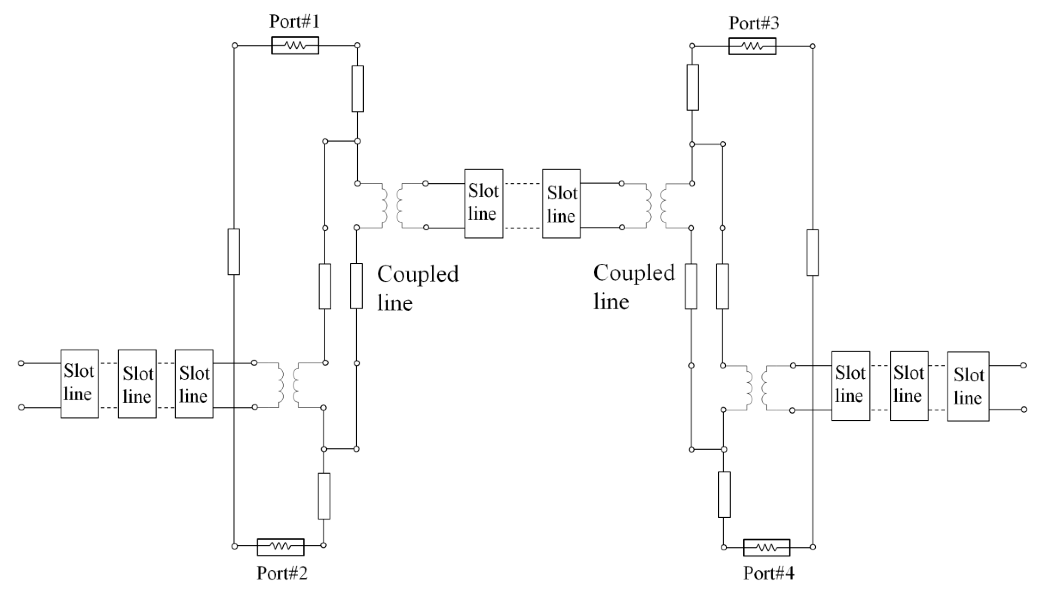
Figure 3.
Equivalent circuit of the meander gap.

Figure 4.
Transmission line equivalent circuit of the meander gap.

Figure 5.
S31 (near-end crosstalk) and S41 (far-end crosstalk) of the meander split plane with length l3 and w1 changed. (a) S31; (b) S41.
Figure 5.
S31 (near-end crosstalk) and S41 (far-end crosstalk) of the meander split plane with length l3 and w1 changed. (a) S31; (b) S41.

Figure 6.
Crosstalk equivalent circuit of the meander split on the ground plane.

Figure 7.
Scattering parameters of the simulation (circuit model) and measured result. (a) S11; (b) S21; (c) S31; (d) S41.
Figure 7.
Scattering parameters of the simulation (circuit model) and measured result. (a) S11; (b) S21; (c) S31; (d) S41.


Figure 8.
Lateral wave attenuation of the unit cell of the meander slot line obtained by Figure 4. (a) Split gap width w2 changed (when l1 = 0.25 mm, l2 = 0.4 mm, l3 = 30 mm, w1 = 2.1 mm, w2 = w3); (b) length l3 changed (when l1 = 0.25 mm, l2 = 0.4 mm, w1 = 2.1 mm, w2 = w3 = 0.2 mm); (c) length l2 changed (when l1 = 0.25 mm, l3 = 2 mm, w1 = 2.1 mm, w2 = w3 = 0.2 mm); (d) number of cells changed (when l1 = 0.25 mm, l2 = 0.4 mm, l3 = 30 mm, w1 =2.1 mm, w2 = w3 = 0.2 mm.

Figure 9.
Current distributions on the straight and meander split power or ground plane at 2 GHz. (a) Straight split plane; (b) meander split plane.
Figure 9.
Current distributions on the straight and meander split power or ground plane at 2 GHz. (a) Straight split plane; (b) meander split plane.

Figure 10.
Time simulation of the crosstalk signal of the straight and meander split ground plane.

Figure 11.
Time domain simulation result of Figure 10.
Figure 11.
Time domain simulation result of Figure 10.

Figure 12.
Comparison of the transmission and crosstalk signal with the straight and meander split power or ground plane. (a) Transmission signal measured at port #2; (b) near-end crosstalk signal measured at port #3; (c) far-end crosstalk signal measured at port #4.
Figure 12.
Comparison of the transmission and crosstalk signal with the straight and meander split power or ground plane. (a) Transmission signal measured at port #2; (b) near-end crosstalk signal measured at port #3; (c) far-end crosstalk signal measured at port #4.


Table 1.
Characteristic impedances and relative dielectric constants of the meander slot line.
| ltot(mm) | l1(mm) | l2(mm) | l3(mm) | w1(mm) | w2(mm) | w3(mm) | Z1(Ω) | Z2(Ω) | Z3(Ω) | εe1 | εe2 | εe3 |
|---|---|---|---|---|---|---|---|---|---|---|---|---|
| 35 | 0.25 | 0.4 | 5 | 14.6 | 0.2 | 0.2 | 168 | 75 | 75 | 1.1 | 1.3 | 1.3 |
| 35 | 0.25 | 0.4 | 15 | 9.6 | 0.2 | 0.2 | 149 | 75 | 75 | 1.1 | 1.4 | 1.4 |
| 35 | 0.25 | 0.4 | 30 | 2.1 | 0.2 | 0.2 | 106 | 75 | 75 | 1.1 | 1.4 | 1.4 |
© 2019 by the author. Licensee MDPI, Basel, Switzerland. This article is an open access article distributed under the terms and conditions of the Creative Commons Attribution (CC BY) license (http://creativecommons.org/licenses/by/4.0/).
Share and Cite
MDPI and ACS Style
Lee, J.-H. A Novel Meander Split Power/Ground Plane Reducing Crosstalk of Traces Crossing Over. Electronics 2019, 8, 1041. https://doi.org/10.3390/electronics8091041
AMA Style
Lee J-H. A Novel Meander Split Power/Ground Plane Reducing Crosstalk of Traces Crossing Over. Electronics. 2019; 8(9):1041. https://doi.org/10.3390/electronics8091041
Chicago/Turabian StyleLee, Jung-Han. 2019. "A Novel Meander Split Power/Ground Plane Reducing Crosstalk of Traces Crossing Over" Electronics 8, no. 9: 1041. https://doi.org/10.3390/electronics8091041
Note that from the first issue of 2016, this journal uses article numbers instead of page numbers. See further details here.