A Low-Cost CPW-Fed Multiband Frequency Reconfigurable Antenna for Wireless Applications


1
Department of Telecommunication Engineering, University of Engineering and Technology, Taxila 47050, Pakistan
2
Department of Electrical Engineering, Polytechnique Montreal, Montreal, QC H3T 1J4, Canada
3
Department of Electronic Systems, Royal Institute of Technology (KTH), Isafjordsgatan 26, SE 16440 Stockholm, Sweden
4
Department of Information Technology, TUCS, University of Turku, Turku 20520, Finland
*
Author to whom correspondence should be addressed.
Electronics 2019, 8(8), 900; https://doi.org/10.3390/electronics8080900
Submission received: 21 July 2019
/
Revised: 9 August 2019
/
Accepted: 13 August 2019
/
Published: 14 August 2019
(This article belongs to the Special Issue Antennas and Propagation Aspects for Emerging Wireless Communication Technologies)
Abstract
:A novel, cedar-shaped, coplanar waveguide-fed frequency reconfigurable antenna is proposed. The presented antenna uses low-cost FR4 substrate with a thickness of 1.6 mm. Four PIN diodes are inserted on the antenna surface to variate the current distribution and alter the resonant frequencies with different combinations of switches. The proposed antenna is fabricated and measured for all states, and a good agreement is seen between measured and simulated results. This antenna resonates within the range of 2 GHz to 10 GHz, covering the major wireless applications of aviation service, wireless local area network (WLAN), worldwide interoperability for microwave access (WiMAX), long distance radio telecommunications, and X-band satellite communication. The proposed antenna works resourcefully with reasonable gain, significant bandwidth, directivity, and reflection coefficient. The proposed multiband reconfigurable antenna will pave the way for future wireless communications including WLAN, WiMAX, and possibly fifth-generation (5G) communication.
1. Introduction
The antenna is considered a vital component for every wireless communication system nowadays. To meet the requirements of different applications in one device, multiband antennas, wideband antennas, and reconfigurable antennas have served this purpose. These individual devices can have many uses, e.g., for global positioning systems (GPS), global system for mobile communication (GSM), Bluetooth, wireless local area network (WLAN), etc. Antenna size and cost are two significant factors when designing any sort of antenna.
Reconfigurable antennas are found to be the best solution, as they can be reconfigured to resonate on different frequencies to provide various functions. Reconfigurable antennas also offer unique advantages, such as flexibility and compactness. Reconfigurable antennas can modify their properties such as frequency, polarization, and radiation pattern with changing environmental conditions or varying system requirements in a controlled manner [1]. A comprehensive and detailed review regarding microstrip reconfigurable antennas has been provided by Shakhirul et al. [2]. Different modern techniques for reconfiguration have been analyzed and the pros and cons are discussed. Methods of improving the switching capability and achieving operation at different frequency bands are discussed and investigated.
Frequency reconfigurable antennas are advantageous for diverse applications, as the need for the bandwidth of spread-spectrum signals is decreased. This is because all operating frequencies are not supposed to be covered by a wireless application simultaneously. As a result, the functionality of the antenna is improved by keeping the size small and less complicated [3]. In frequency reconfigurable antennas, low cost, miniaturized size, and use for various applications are other necessary characteristics that result in their incorporation in maximum modern wireless communication systems [4].
Many types of techniques for feeding have been reported, but the coplanar waveguide (CPW) feeding technique has been the most preferable. It reduces the complexity in design by employing the antenna patch and the ground plane on the same side of the substrate.
Several researchers have attained frequency reconfiguration by changing the operative length of the antenna by removing or adding part of its length by using various approaches, such as varactors or variable capacitors [5]. Varactor diodes are used to redirect surface current, therefore letting a smooth change in frequency with altering capacitance [6]. The authors presented a varactor-based reconfigurable antenna with the capability to operate in the tuning range from 890 to 1500 MHz with good impedance matching [7]. This antenna is very promising because the multiple smaller patches are connected by means of varactors which permit polarization agility, frequency tuning, and phase shifting. Likewise, Korosec et al. [8] presented a different multisubpatch microstrip antenna loaded with varactors for solving the reconfiguration problem.
A cedar-shaped reconfigurable antenna was designed for operation in WiMAX, Bluetooth, GPS, and WLAN bands [9]. Both PIN and varactor diodes are used in combination to achieve the reconfigurability. Three pairs of varactor diodes were utilized for achieving such an objective. Due to the utilization of so many varactor diodes with different variations, it becomes very lossy as the varactors used were from two different manufacturers, including SMV1211 from SKYWORKS and 1SV325 from TOSHIBA. Also, the overall size of the antenna is very bulky, and the total board size is 6.5 × 6 cm2. However, varactor diodes are considered undesirable as they are nonlinear and exhibit a narrow tuning range [10]. Likewise, the authors proposed a varactor-based antenna with a tuning range from 2.34 to 2.68 GHz [11]. Such tuning is achieved by changing the varactor diode capacitance between 12.33 pF (0 V) to 1.30 pF (15 V). Babakhani et al. [12] reported a tunable wideband frequency with polarization reconfiguration. The antenna performed in a continuously switching frequency range from 1.17 to 1.58 GHz by loading the varactor between the patch and the ring.
Reconfiguration using RF-MEMS gave lower loss and increased Q factor compared to PIN diodes and varactors [13]. Amongst these switching techniques, PIN (Positive-Intrinsic-Negative) diodes are considered to be low cost with sound isolation, easy fabrication, and low insertion loss for optimal performance. They are very consistent and compact as they tend to increase switching speeds and decrease resistive capacitance in both states, i.e., ON and OFF. CPW feed slot and folded slot antennas have been reconfigured to alter the resonant frequency by switching the slot length [14].
Previous reported works have utilized bias lines or vias for activation of PIN diodes, which make the circuit complicated and degrade the performance of the overall antenna system. Therefore, in this work, the biasing circuit is integrated into the same antenna to make it simple, and no vias are used. The effective length of the antenna is controlled by PIN diodes.
Han et al. [15] reported L-shaped and U-shaped slots using three pin diodes for long term evolution (LTE) and WLAN applications, whereas its substrate has an antenna element on both sides. A pattern and frequency reconfigurable microstrip-based antenna is presented that has three operational states using five pin diodes; unidirectional at 5.4 GHz, omnidirectional at 2.4 GHz, and both unidirectional and omnidirectional functionalities operate simultaneously [16]. Similarly, three pin diodes are implanted on the ground plane of a frequency reconfigurable antenna to control switching states [17]. Its radiating patch is designed as a square for WLAN, WiMAX, and Bluetooth applications. The FR4-based frequency reconfigurable antenna presented by Liu et al. [18] resonates between different modes, i.e., narrow band, ultra-wideband, and dual-band. The ground is slotted with four pin diodes that result in switching. Five PIN diodes are embedded in the microstrip frequency reconfigurable antenna, with six states switchable between 2.2 GHz to 4.75 GHz [19]. However, there are three drawbacks in the design; complexity due to the large number of switches; large size; and low impedance bandwidth. It must be noted that the concept of achieving wideband performance from the tapered structure is based on [20,21], where the authors utilized a printed tapered monopole antenna (PTMA) and investigated the ultra-wideband (UWB) behavior. They showed their step by step approach to bandwidth dispensation from corresponding rectangular to tapered and then from circular/cylindrical to tapered structures. They also compare the bandwidth performance in each case.
Therefore, in this paper, a CPW-fed, compact, cedar-shaped, multiband frequency reconfigurable antenna is proposed. The main advantage of this antenna is its ability to tune to different resonant frequencies. The length of the radiating patch is changed by the lumped elements, mainly PIN diodes in this design, to achieve different resonant frequencies ranging from 2 GHz to 10 GHz.
The paper is arranged in the following manner. Section 2 gives step by step guidelines and the approach used in designing the proposed antenna. Section 3 investigates and provides the refined antenna’s simulated vs. measured results in different scenarios. Section 4 compares the proposed work with the recently published state of the art designs in the literature, which is followed by a conclusion section.
2. Step by Step Design Guidelines and Approach
2.1. Antenna Geometry
The corresponding geometrical dimensions of the proposed multiband reconfigurable antenna is displayed in Figure 1. This antenna utilizes a low-cost FR4-Epoxy substrate with loss tangent tan δ = 0.02, dielectric constant εr = 4.4, and thickness of 1.6 mm. The overall dimensions of the antenna are 40 × 60 mm2. The antenna design modeling is carried out in a commercially available FEM (Finite element method)-based simulator, ANSYS HFSS. Moreover, we have also validated our results on time domain-based simulator CST (FDTD) before fabrication and measurement.
To achieve improved impedance matching and acceptable gain, the shape of the main radiating patch resembles the cedar tree and the rectangular slots are placed over an equilateral triangle. The antenna is designed in such a way to resonate on different frequency bands, using four PIN diodes, named 2, 3, 4, and 5, with a lumped element boundary in a reserved slot of 1 mm. The width of the CPW feedline is 1 mm to excite the antenna with the characteristic impedance of 50 Ω. This value of CPW feedline is evaluated by using Equations (1)–(6) [22].
The parameters used in these equations are described as follows: Sc is the width of the central conductor, Zocp is the characteristic impedance of the CPW line, W is the separation between the central conductor and ground plane, εr is the relative dielectric constant of the substrate, εeff is an effective dielectric constant, h is the thickness of the substrate, K1, and K2 can be calculated by utilizing Sc, W, h, a, and b as defined before. K(k) is defined as the integral of first order with argument k or complementary argument k′.
Table 1 displays the optimized overall dimensions of the antenna. Transmission line theory is used to calculate the effective length for a specific resonating frequency using Equation (7) taken from [23].
where h is the thickness of the substrate, c is the speed of light, Lr is the length of the resonant frequency, and εr is the relative permittivity of the substrate.
2.2. Design Methodology
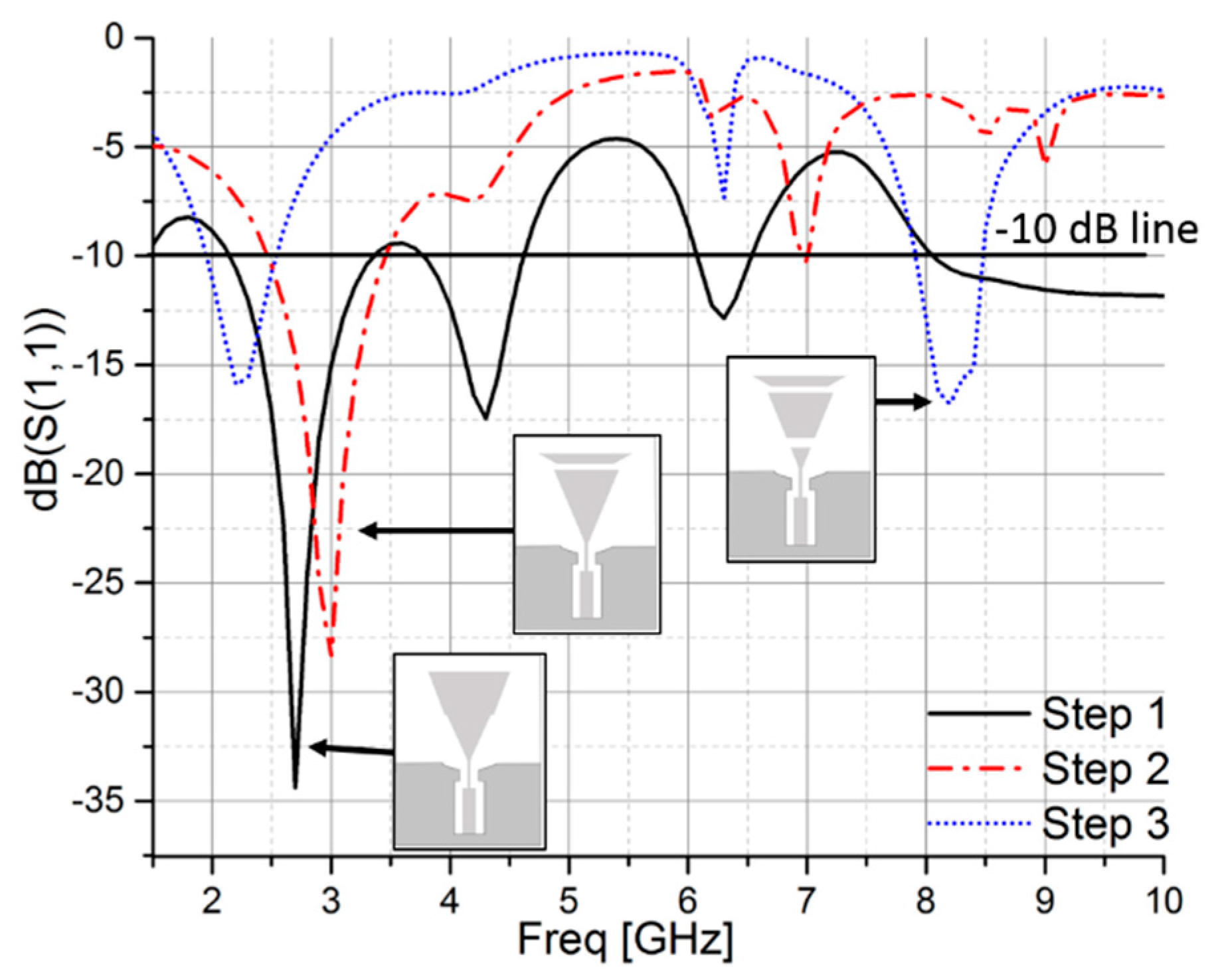
Figure 2 shows the steps to achieve the cedar-shaped antenna at different operating modes with its corresponding S11, which basically represents how much power is reflected from the antenna, and hence is known as the reflection coefficient [22]. The minimum value of |S11| is 0 (best case and corresponding dB value is –∞), the maximum value of |S11| is 1 (worst case and corresponding dB value is 0), and the compromised/acceptable value of |S11| is 0.33 (corresponding dB value is almost –10). As can be seen in our simulations, the corresponding S11-parameter value is less than −10 dB in all passbands. Parametric analysis of the antenna is performed based on the corresponding S11. To perform it, first, an occupied equilateral triangle is designed as a basic structure with a CPW feedline. In this case, the electrical length is large, and the current is flowing through the whole antenna, thus making it resonate at multiple frequencies, i.e., 2.7 GHz, 4.3 GHz, and 6.2 GHz. Secondly, a strip is defined at the upper side of the equilateral triangle which results in a frequency shift at 3 GHz. In the last case, the lower part of the equilateral triangle is disjoined from the previous design to obtain a higher frequency, i.e., 8.2 GHz, as the current path becomes shorter compared to other cases. All these variations with corresponding reflection coefficient plots are shown in Figure 1.
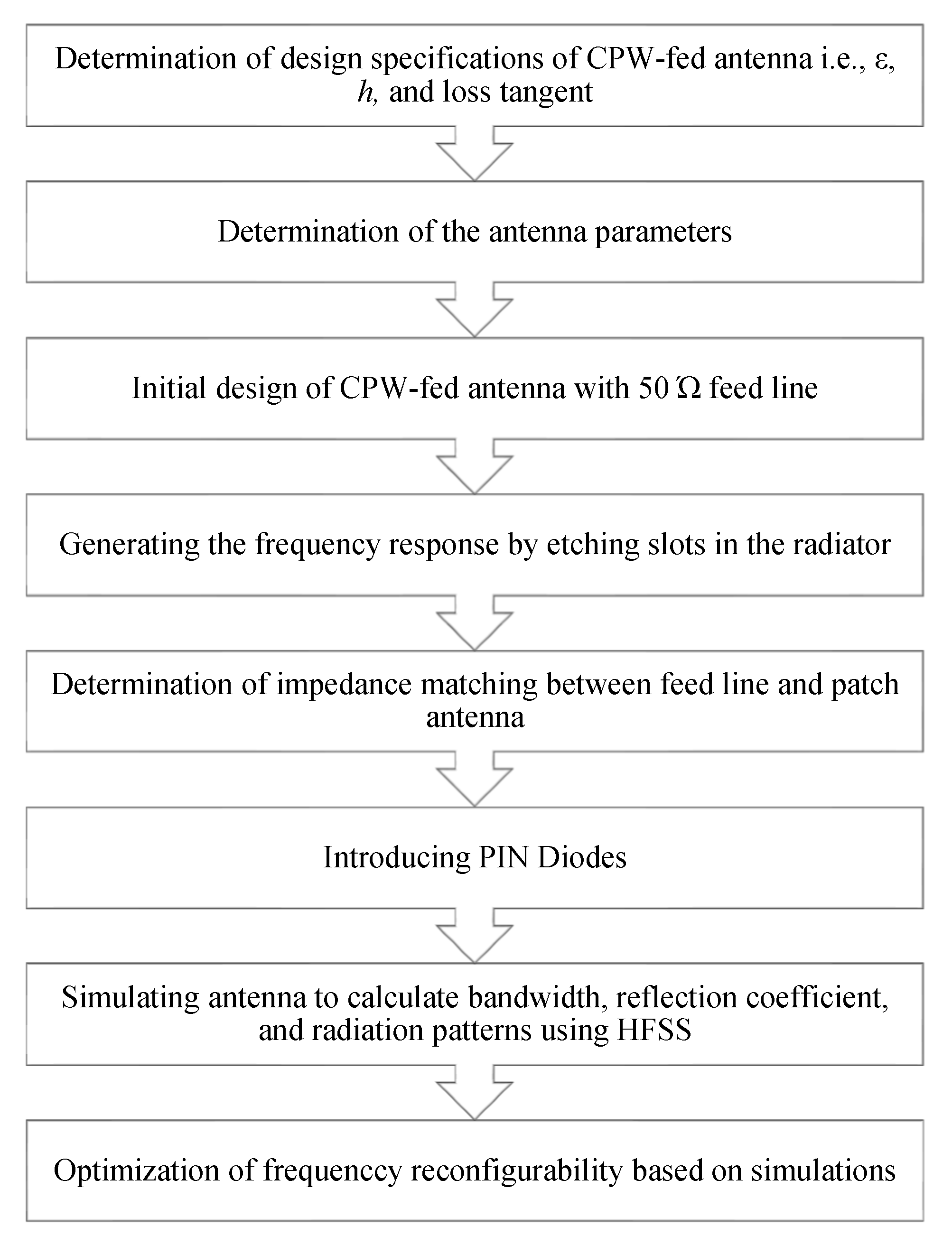
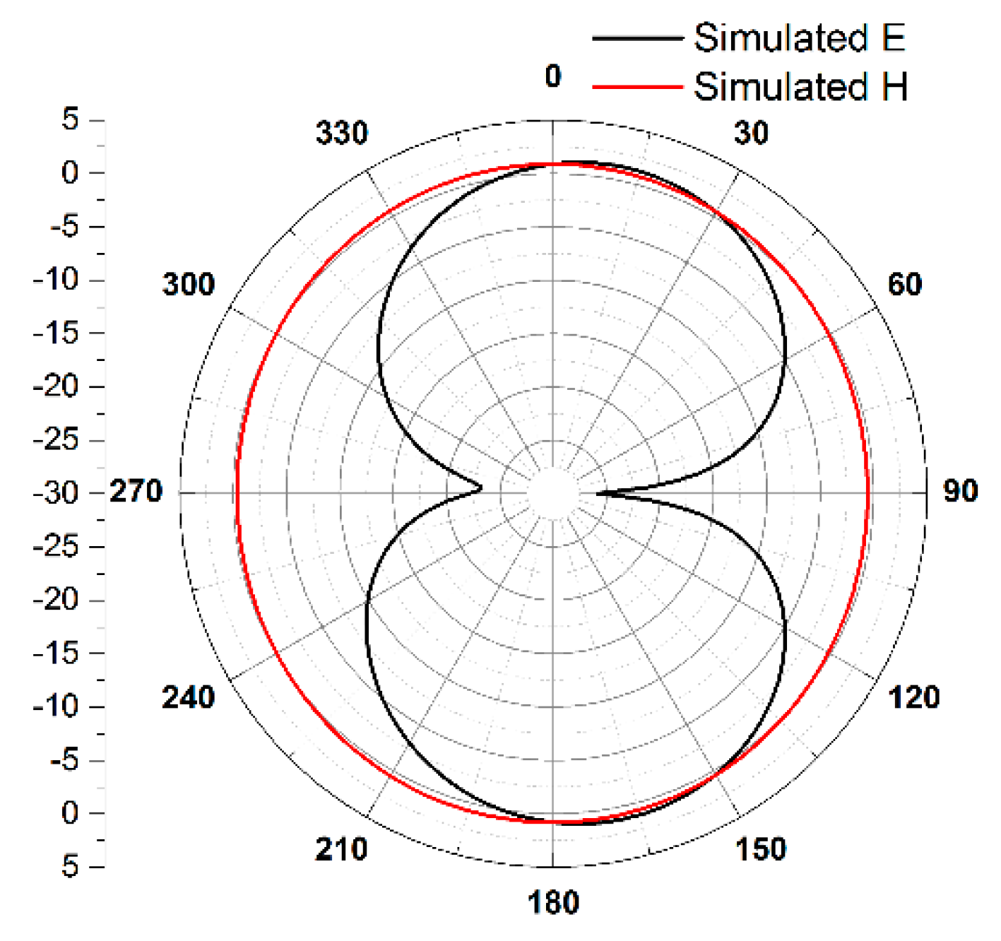
The ultimate proposed design is obtained by the incorporation of four PIN diodes (2, 3, 4, 5) at specified locations. The diodes are termed as S with 1 mm reserved slots between the upper and middle portion of the equilateral triangle. This results in frequencies ranging from 2 GHz to 10 GHz. A flow chart demonstrating the steps taken to achieve the desired design is shown in Figure 3. The corresponding radiation pattern, including both principal planes for the fundamental structure, is shown in Figure 4.
2.3. Switch Design
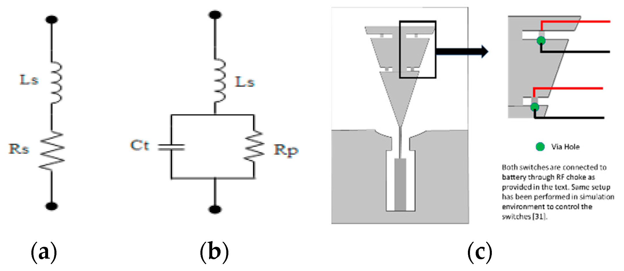
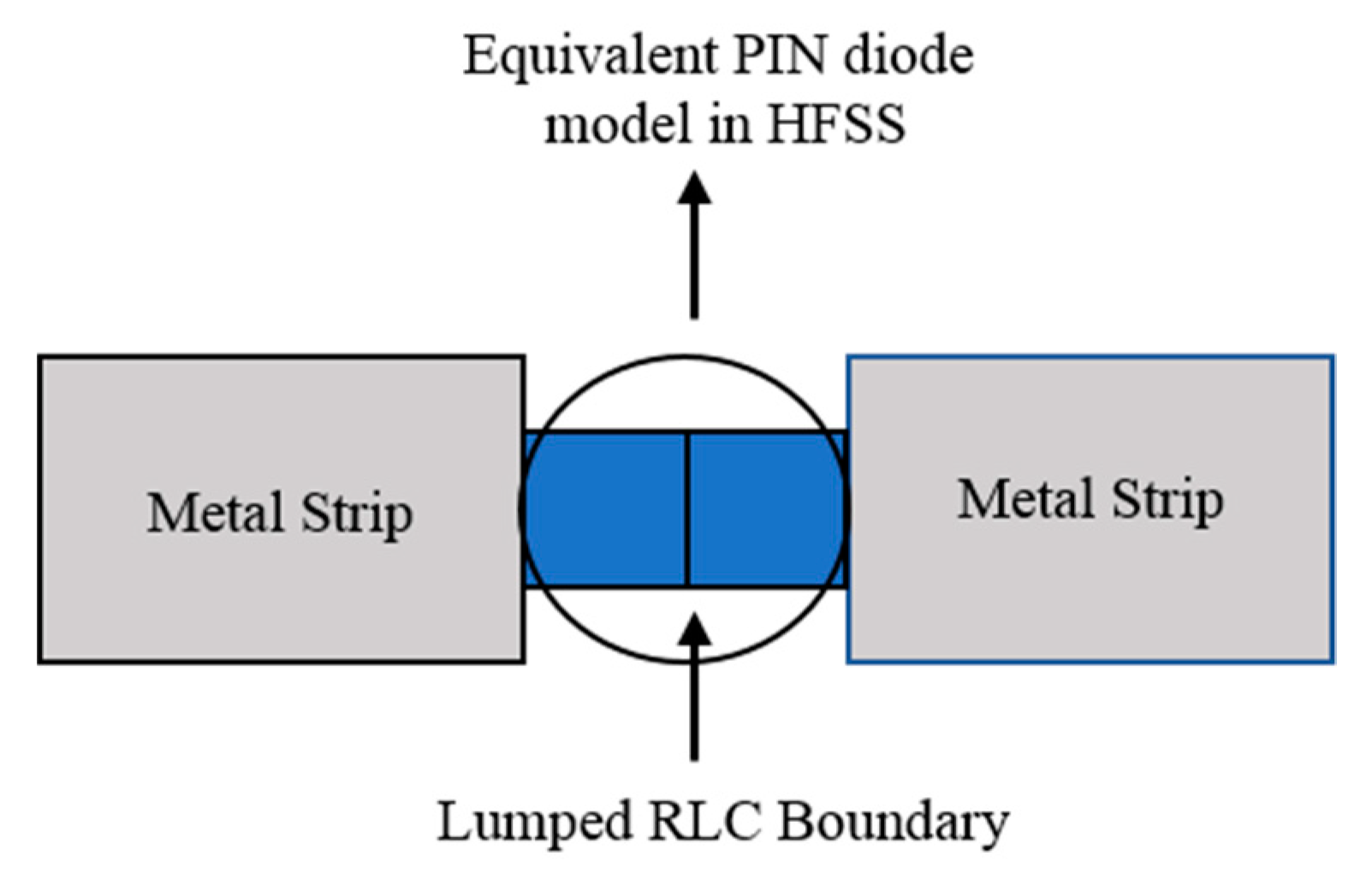
To confer electronic reconfigurability, model shunt switches were substituted with PIN diodes. These PIN diodes are suitable for reconfiguration owing to their reliability, low cost, high switching speed, small size, and decreased capacitance and resistance in the ON and OFF states. Figure 5a,b illustrates both the ON and OFF states in that order. The reactive components Ct and Ls produce the packaging impact, while others develop the electronic traits in the ON and OFF states of the diode junction. Referring to the datasheet of PIN diode SMP 1320-079, the lumped characteristics for the ON state are Ls = 0.7 nH, Rs = 0.9 Ω. In the OFF state (reverse biased), Rp is given a higher value than the reactance Ct because of packaging; therefore, it is ignored from the equivalent diode model.
It is noteworthy that during the simulation process in HFSS, a strip element of size around 1 mm × 1 mm was used to characterize the PIN diode, and its equivalent circuit in the ‘‘ON’’ and ‘‘OFF’’ states is as shown in Figure 5a,b, respectively. The reason for using a PIN diode in this work is because the PIN diode has better RF switching capability [23]. Notably, removing this strip element during the simulation to indicate the ‘‘OFF’’ state has also been investigated, and the results are very similar to applying the lumped element as in Figure 5. Thus, in the following simulation, the latter technique was used. To maintain good DC isolation in practical scenarios, four RF chokes (inductors with 1 µH) must be used in the DC biasing circuit, and they need to be linked to a two separate two-position dual inline package (DIP) switch and a low-power lithium battery (approximately 3 volts DC and a continuous standard load current of 0.2 mA). However, it must be noted that the DC supply is to be protected from RF. DC blocking is done using an appropriate capacitor and RF blocking is done using an RF choke. Values of capacitance and inductance are based on the operating frequency.
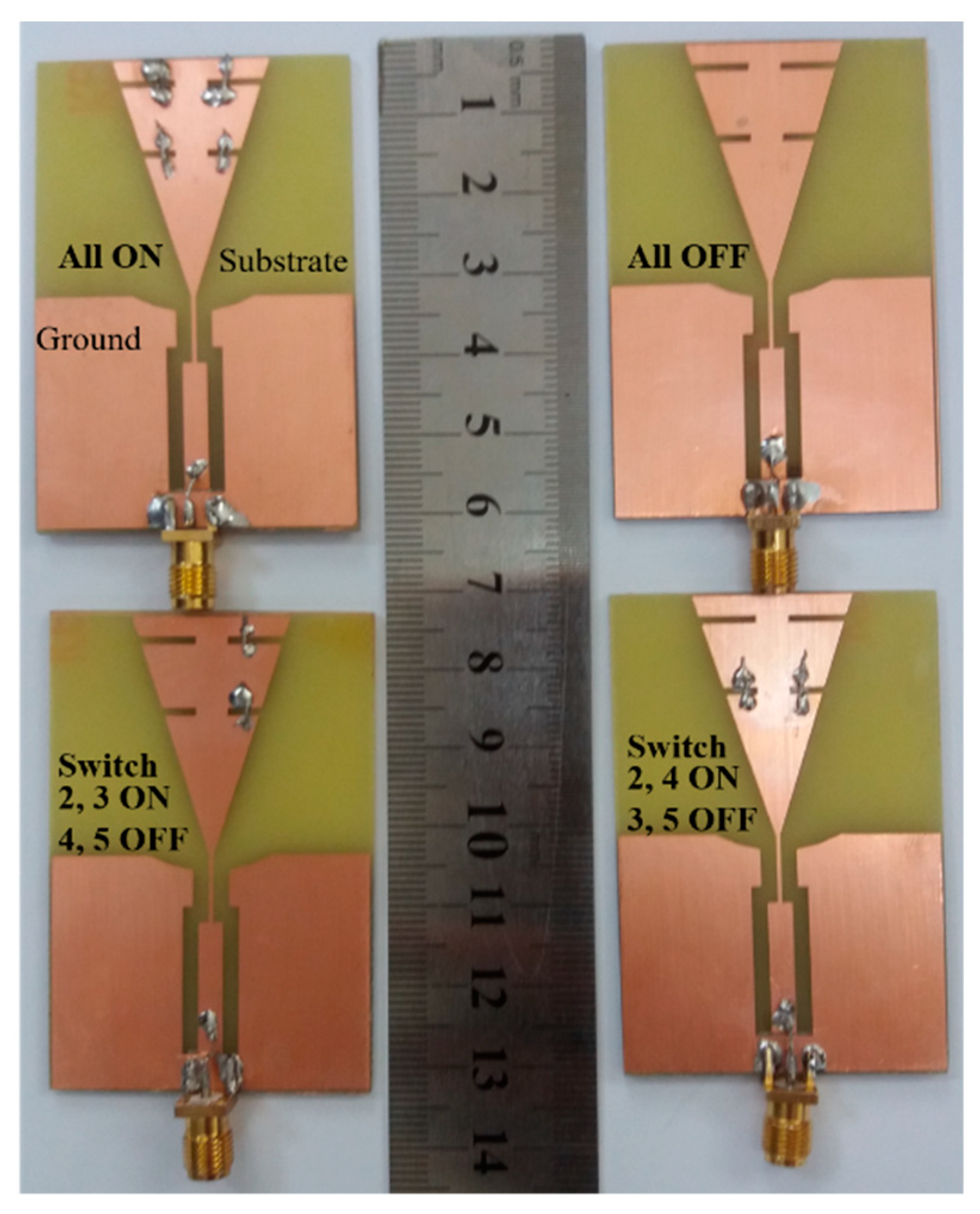
For clarity and simplicity, we employed a simple strip that can turn on and off the switch for demonstration. For further use in practical applications, the biasing circuit of Case 3 is provided, which is very simple to predict. The switch is connected to the 3 V battery and the two terminals are considered, one with a via hole and the other through an RF choke of 1 µH. A strip has been placed on the back side for via connection through the battery and can be soldered in the same way as in [24,25]. A similar procedure has been adopted for Case 4. All these cases were first studied in a simulation environment in order to determine the possible states. In fabrication, different antennas are designed for each case in order to clearly distinguish them and so that the reader may understand the step by step approach. All cases are measured, and the results are provided in each case. Only states that have an independent feed are considered and placed in the manuscript. A canonical model of Case 3 is also provided in Figure 5c for further illustration.
In the proposed antenna design, modeling of the PIN diode in HFSS has been done by employing two sets of lumped RLC boundary conditions, as shown in Figure 6. L is the first portion of this RLC model and the second is a parallel combination of Rp and Ct for the OFF state or Rs for ON state, respectively. Ansoft HFSS (High Frequency Structure Simulator) is used for modeling of the PIN diodes, which provides robustness regarding reconfiguration among several resonating frequency bands.
3. Results and Discussions
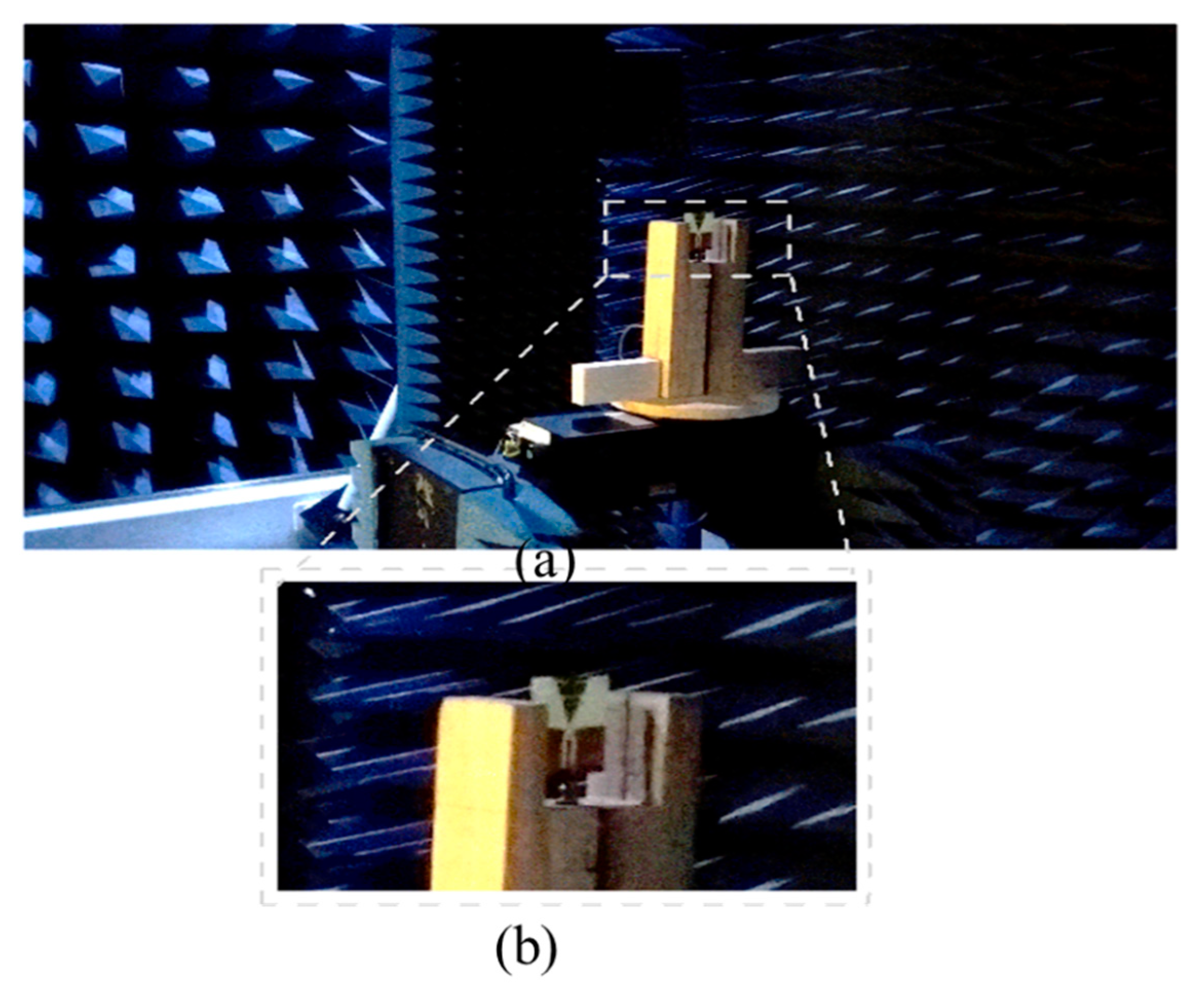
For validation of the performance parameters of the designed antenna, a prototype was fabricated for all four cases, as shown in Figure 7, and measured. A vector network analyzer was used for measurement of the reflection coefficient and VSWR. The antenna radiation pattern is measured using the anechoic chamber installed in the NUST research center for microwave and millimeter waves (RIMMS). The chamber can characterize antennas in the frequency range from 0.8 GHz to 40 GHz. The anechoic chamber is equipped with a near-field planner scanner and a far-field tower to measure the radiation pattern of a given antenna under test (AUT). The measurement software has the capability to transform the near-field data to far-field data for plotting antenna radiation patterns in 3D. A snapshot of the measurement setup in the anechoic chamber of the proposed antenna is shown in Figure 8a while the zoom in view is shown in Figure 8b.
The general states of the achieved bands and positions relating to the various configurations of the PIN diodes are depicted in Table 2. The electrical length of the presented antenna is characterized by the switch’s ON/OFF states that radiate at a particular frequency band. In the Table ‘0’ represents the OFF state, whereas ‘1’ represents the ON state. The best possible results out of the 16 tested states were chosen for the manuscript. The four states mentioned in the paper have outstanding characteristic parameters, including VSWR less than 2, wide bandwidth, reasonable gain, and excellent radiation efficiency at all operating frequencies. The reflection coefficient at all states is below −10 dB, which confirms that the antenna operates properly. The antenna parameters were also theoretically calculated using the below-stated Equations (8)–(12) [26,27,28,29]. The calculated values are approximately the same as of the experimentally obtained values.
The variables from the above equations are described as follows: Г is reflection coefficient, LRT is the return loss, Za is input impedance of the antenna, RL is the loss resistance, and Rr is the radiation resistance of the antenna.
Along with above-mentioned antenna features, effective aperture is one of the critical parameters to calculate because the surface current and field intensity at the aperture of the antenna is not uniform. The effective aperture of the antenna is theoretically calculated from Equation (13) [30]. To obtain gain and directivity, D values for the proposed antenna were determined. ηap is the aperture efficiency, Ap is the physical aperture, and Ae is the effective aperture of the antenna.
It should be noted that physical aperture Ap is always less than the effective aperture Ae.
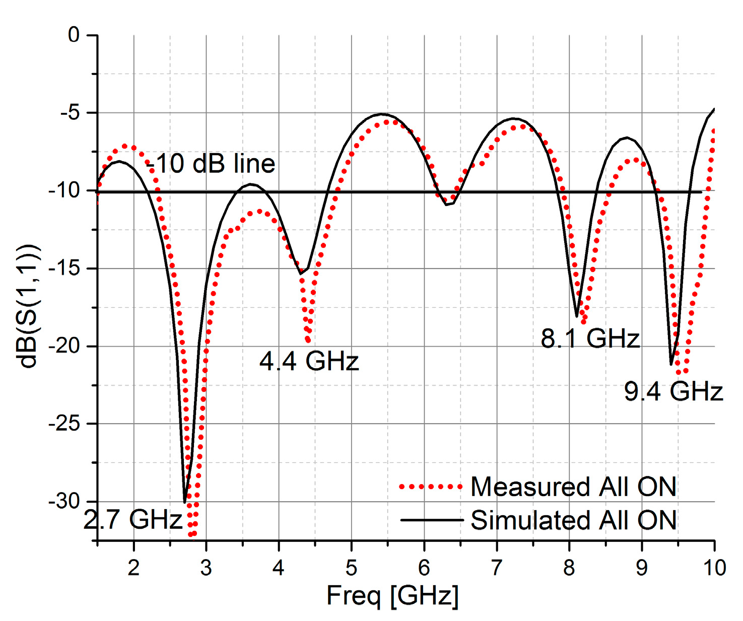
3.1. Case 1: (All Switches ON)
The measured and simulated S11 in Case 1 are shown in Figure 9. All the switches are ON in this case; thus, current pass through the longest path and all parts of the antenna radiates. In this mode, the antenna resonates at four different operating bands from 2.2 GHz to 9.7 GHz. This band has almost same radiation pattern, i.e., the omnidirectional pattern in H-plane and bidirectional in E-plane, as all its frequency bands, so a radiation pattern that is appropriate for all frequencies is selected for inclusion in the paper. This antenna is an excellent choice for integration into portable devices for wireless communication. Figure 10 shows the radiation pattern for all switches in the ON state.
The first band is from 2.2 GHz to 3.4 GHz with a mid-operating frequency of 2.7 GHz and an impedance bandwidth of 1200 MHz. It covers the WLAN standards of 2.4 GHz to 2.484 GHz and WiMAX standards of 2.5 GHz to 2.69 GHz. The second band is from 3.8 GHz to 4.7 GHz with an operating frequency of 4.4 GHz and an impedance bandwidth of 900 MHz. This band covers a part of the S-band. The S-band is used for weather radar, surface ship radar, and some communications satellites (WLAN, Bluetooth, ZigBee, radio astronomy, microwave devices/communications, mobile phones, GPS, amateur radio).
The C-band is used for long-distance radio telecommunications. Mostly 4.4 GHz is used for defense communication. The third band achieved is from 7.8 GHz to 8.4 GHz with an operating frequency of 8.1 GHz and an impedance bandwidth of 600 MHz. This band covers an essential part of the X-band for wireless communication. It includes the military demand for satellite uplinks and the mobile satellite sub-band from 7.9 GHz to 8 GHz for naval and land mobile satellite earth stations. The military requirement for earth exploration satellite (downlink) purposes is in the band from 8 GHz to 8.4 GHz. The last band, in this case, starts from 9.2 GHz and ends at 9.7 GHz with an operating frequency of 9.4 GHz and an impedance bandwidth of 500 MHz. It is used for satellite communications, radar, terrestrial broadband, space communications, and amateur radio. The summarized results of this case are presented in Table 3.
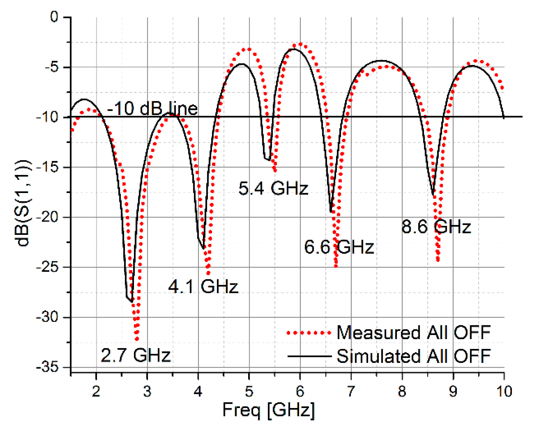
3.2. Case 2: (All Switches Off)
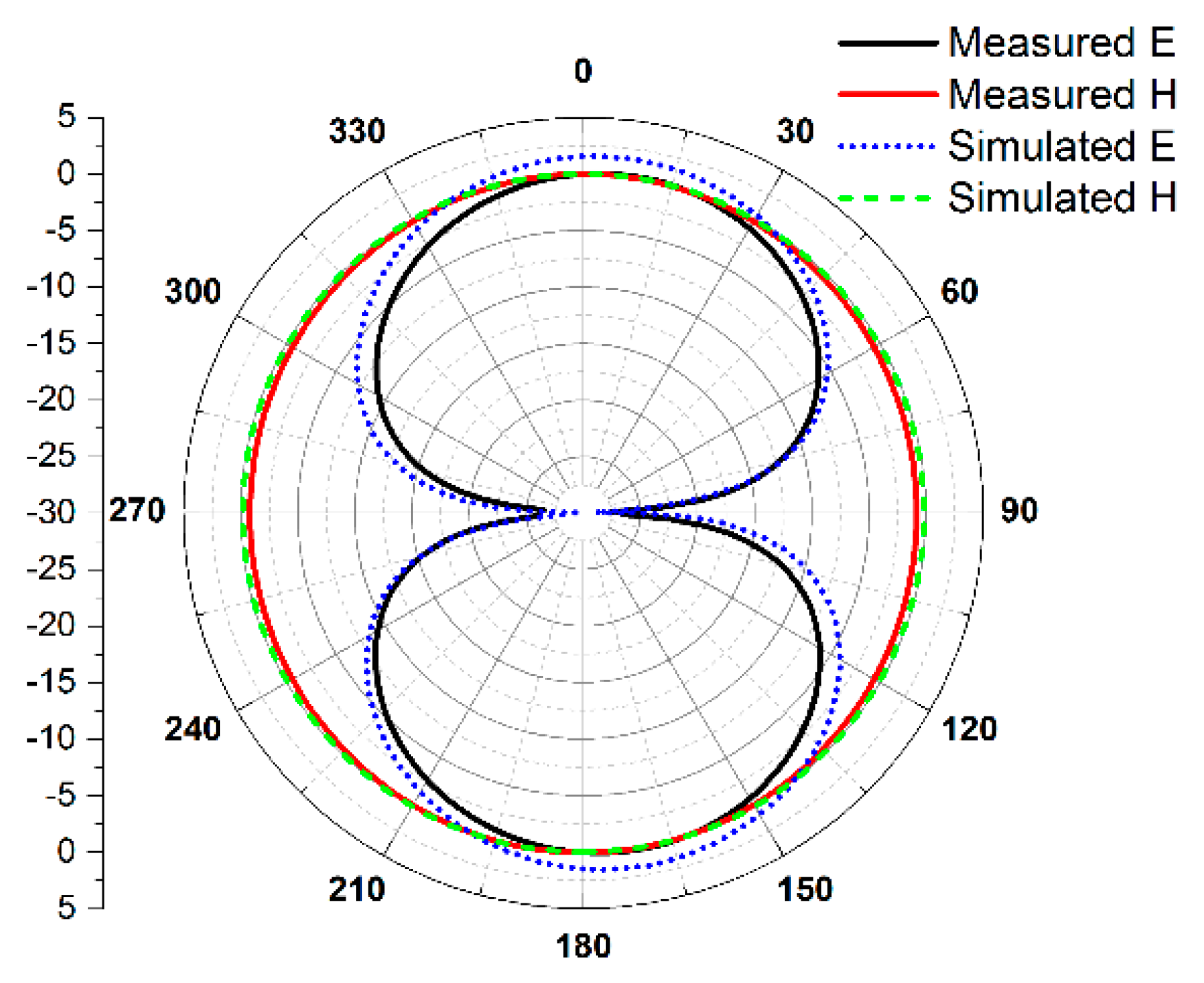
The simulated and measured S11 in Case 2 are depicted in Figure 11. All the switches are OFF in this case; thus, current passes through the shortest path, and part of the antenna resonates. In this mode, the antenna resonates at five different operating bands with an impedance bandwidth of 2.1 GHz to 8.8 GHz. The radiation pattern of this case shows the same behavior, with an omnidirectional pattern in the H-plane and bidirectional in the E-plane as shown in Figure 12.
The first band achieved, in this case, is from 2.1 GHz to 3.3 GHz with an operating frequency of 2.7 GHz and an impedance bandwidth of 700 MHz. This band is used in earth exploration satellites, radio astronomy, and space research services whereas the 2.7 GHz to 2.9 GHz band is used by aviation services. The band from 3.1 GHz to 3.3 GHz band is used in by radiolocation services. This band is allocated for both federal and nonfederal use.
The second band achieved is from 3.6 GHz to 4.3 GHz with an operating frequency of 4.1 GHz and an impedance bandwidth of 700 MHz. This band is useful for WiMAX applications. The third band achieved is from 5.2 GHz to 5.46 GHz with an operating frequency of 5.4 GHz and an impedance bandwidth of 260 MHz. This band can be used mainly for 5.15 GHz to 5.825 GHz standard WLAN applications. The fourth band achieved is from 6.4 GHz to 6.8 GHz with an operating frequency of 6.6 GHz and an impedance bandwidth of 400 MHz. This band is used for long-distance radio telecommunications. The last band of this case covers 8.4 GHz to 8.8 GHz with an operating frequency at 8.6 GHz and an impedance bandwidth of 400 MHz. This band is used for X-band Satellite communication. Table 4 presents the summarized results of this case.
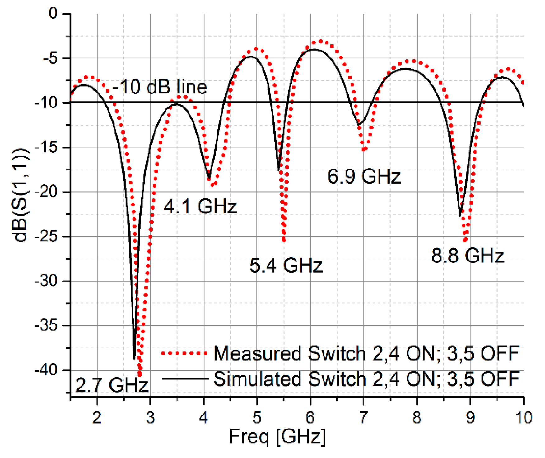
3.3. Case 3: (Switches 2 and 4 ON, Switches 3 and 5 OFF)
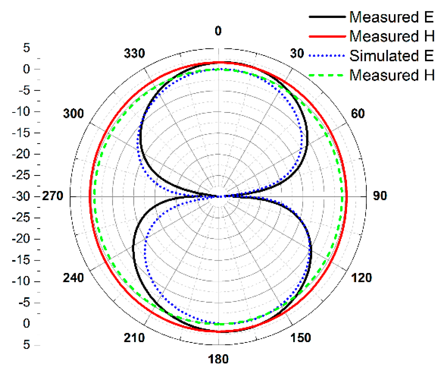
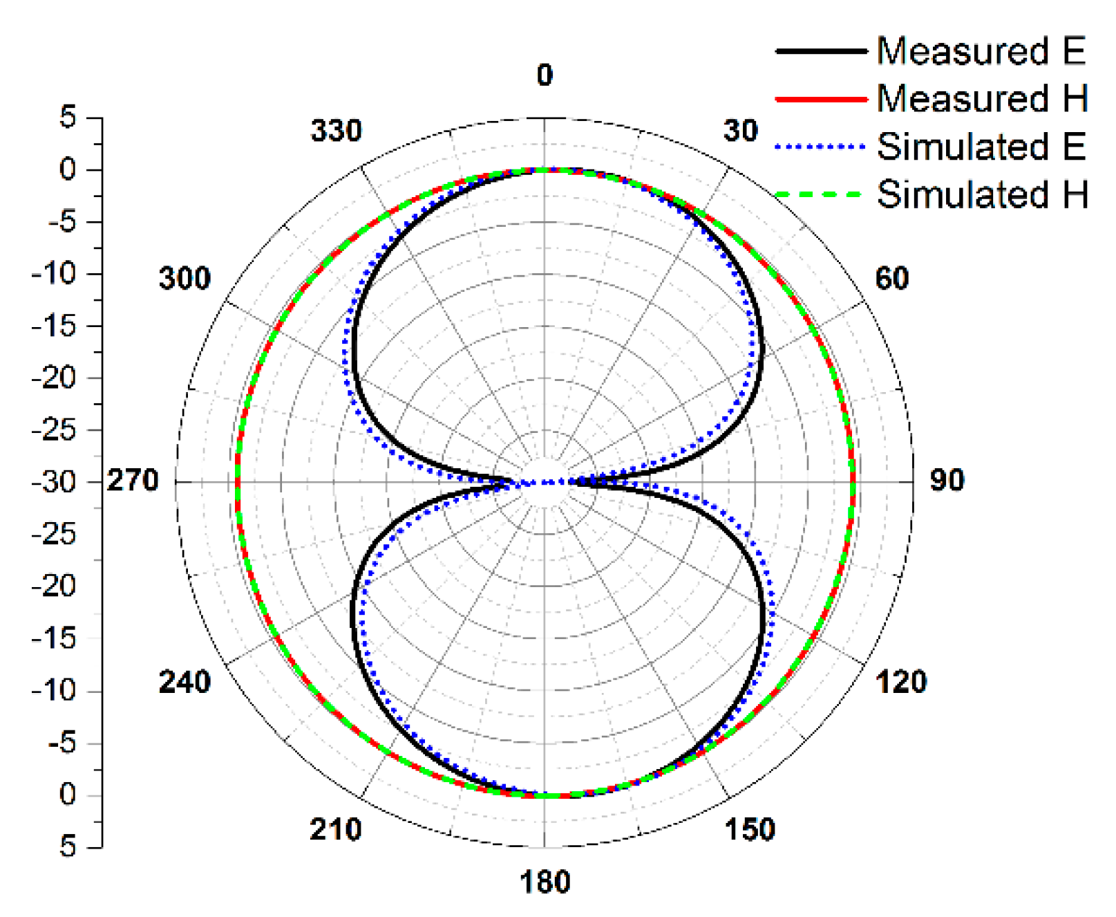
The measured and simulated S11 in Case 3 are shown in Figure 13. Switches 2 & 4 are ON in this case, whereas switches 3 & 5 are OFF; thus, current passes through the upper part of the antenna only. In this mode, the antenna resonates at five different operating bands with an impedance bandwidth of 2.2 GHz to 9.2 GHz. The radiation pattern of this case shows the same behavior, having an omnidirectional pattern in the H-plane and a bidirectional pattern in the E-plane, as shown in Figure 14.
In this case, the first three bands are similar to the previous cases but with slight differences. The fourth band ranges from 6.7 GHz to 7.2 GHz with an operating frequency of 6.9 GHz and an impedance bandwidth of 500 MHz. This band supports fixed satellite communication and WiMAX applications. The last band covers 8.4 GHz to 9.2 GHz with an operating frequency of 8.8 GHz and an impedance bandwidth of 800 MHz. This band is used for satellite and space communications. Table 5 shows the summarized results of this case.
Regarding Case 2 and Case 3, the applications of both cases are different since the variation in frequency is very minor, i.e., Case 2 antennas can be used for aviation services, WiMAX, WLAN, long distance radio communication, and X-band satellite communication, while Case 3 antennas can be used for S-band applications, WiMAX, aeronautical radio navigation services, and X-band satellite communication.
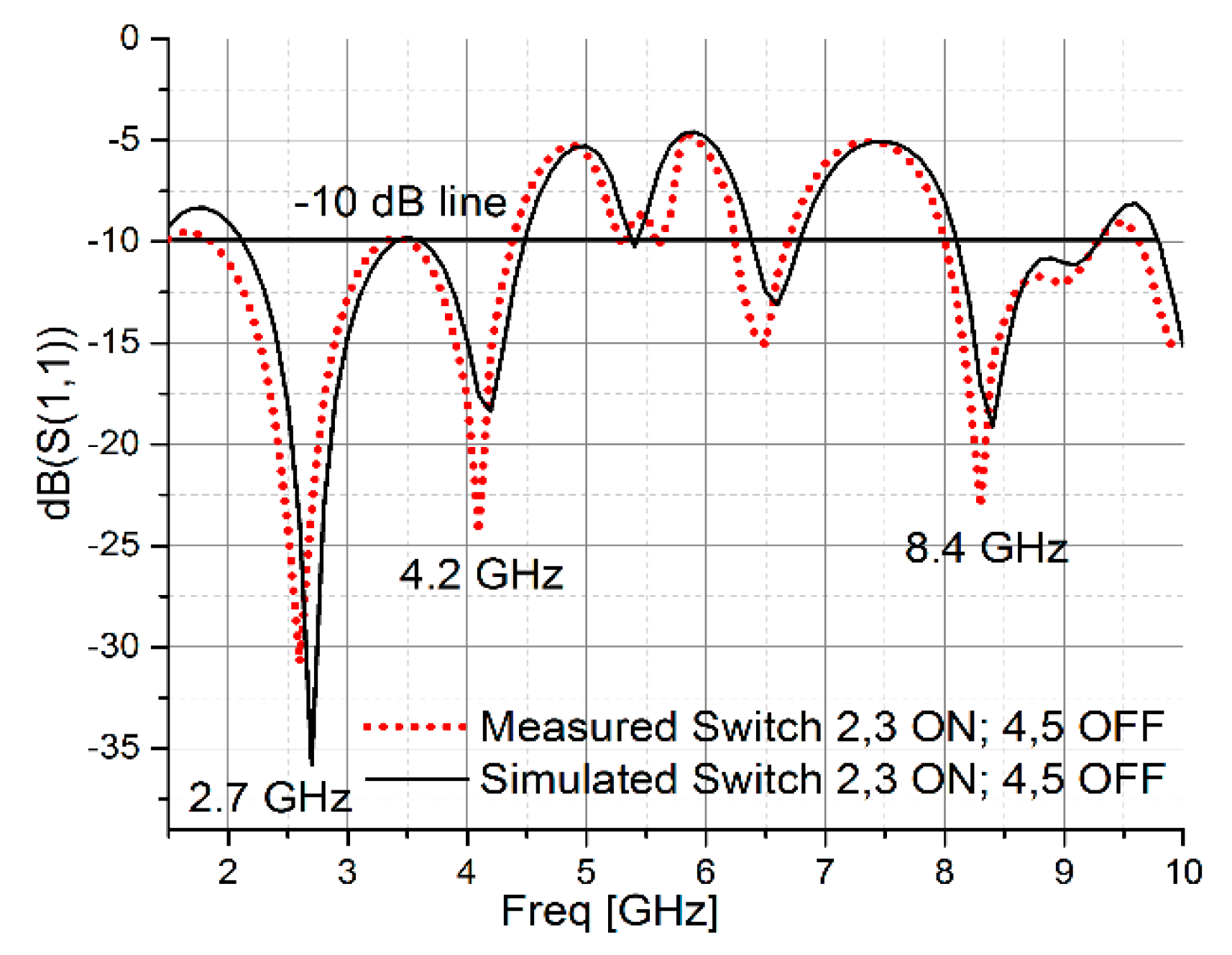
3.4. Case 4: (Switches 2 and 3 ON, Switches 4 and 5 OFF)
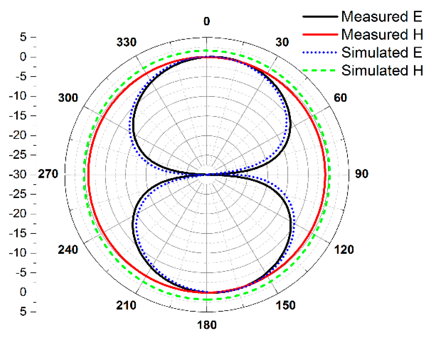
The measured and simulated S11 in Case 4 are shown in Figure 15. Switches 2 & 3 are ON in this case, whereas switches 4 & 5 are OFF; thus, current passes through the right part of the antenna only. In this mode, the antenna resonates at three different operating bands with an impedance bandwidth of 2.2 GHz to 8.8 GHz. The radiation pattern of this case shows the same behavior, having an omnidirectional pattern in the H-plane and bidirectional pattern in the E-plane, as shown in Figure 16.
The first band in this state ranges from 2.2 GHz to 3.3 GHz with an operating frequency of 2.7 GHz and an impedance bandwidth of 1100 MHz. This band is used in the aviation service, maritime service, and the radiolocation service. The second band ranges from 3.7 GHz to 4.5 GHz with an operating frequency of 4.2 GHz and an impedance bandwidth of 800 MHz. This band is used for long-distance radio telecommunications. The last band ranges from 8.1 GHz to 8.8 GHz with an operating frequency of 8.4 GHz and an impedance bandwidth of 700 MHz. This band covers a productive part of the X-band wireless application. The summarized results of this case are given in Table 6.
3.5. Proposed Antenna Gain and Efficiency (%) at Different Stages
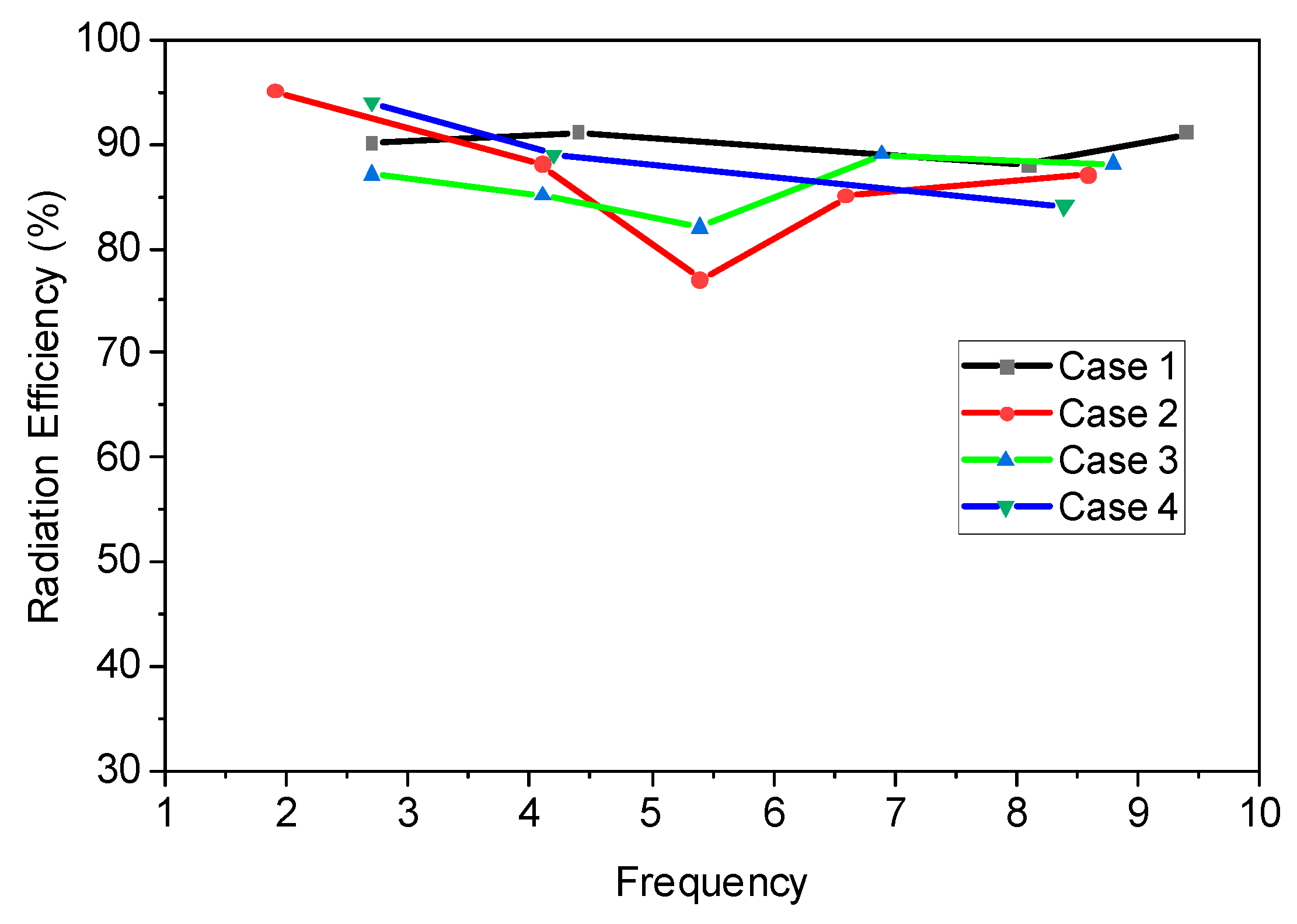
The gain (dBi) and percentage efficiency of the proposed antenna is also taken into account and considered at all four cases. The brief description of the gain is tabulated in Table 7 which shows the gain of the proposed antenna in all four cases at their resonance frequencies. It is seen that the proposed antenna possesses an acceptable gain. Also, a brief description of the antenna efficiency (%) is tabulated in Table 8 and plotted in Figure 17, which shows the percentage radiation efficiency of the proposed antenna in all four cases at their resonance frequencies. It shows that antenna efficiency (%) is very stable in each case at the resonance frequency.
4. Comparison with Other State of the Art Designs
The proposed antenna was compared with the recent state of the art to highlight the novelty of this work. The comparison is summarized in Table 9. It can be seen that the proposed antenna is advantageous in terms of maximum passbands, its wide reconfigurable behavior, low-cost substrate, and overall size.
5. Conclusion
A novel cedar-shaped multiband frequency reconfigurable antenna is proposed for WLAN, WiMAX, X-band satellite, and many other wireless communication systems. The broad tunability of operating bands is achieved by employing switches to alter the effective electrical length of the radiating element of the antenna. The proposed antenna is studied and optimized in different reconfigurable scenarios and validated through measurements. The proposed antenna is studied in terms of important antenna parameters, including reflection coefficient, antenna gain, and radiation pattern, through simulation as well as measurements. This antenna radiates efficiently at all the desired bands. Design simplicity, compactness, and reconfigurability are the features that make this antenna a good choice for future wireless communication applications.
Author Contributions
Conceptualization, T.K.; Data curation, T.K.; Formal analysis, T.K. and M.R.; Investigation, M.R., A.A. and Y.A.; Methodology, T.K. and M.R.; Project administration, Y.A.; Resources, A.A.; Software, A.A.; Supervision, A.A. and Y.A.; Validation, Y.A. and H.T.; Visualization, H.T.; Writing—original draft, T.K.; Writing—review & editing, M.R.
Funding
This research received no external funding.
Acknowledgments
The work was financially supported by Vinnova (The Swedish Governmental Agency for Innovating Systems) and University of Engineering and Technology Taxila, Pakistan through the Vinn Excellence centers program and ACTSENA research group funding, respectively. The fabrication of the antenna has been carried out at National Institute of Electronics (NIE) Islamabad, Pakistan, whereas antenna testing and measurement was done at Research Institute for Microwave and Millimeter-Wave Studies (RIMMS), National University of Science and Technology (NUST), Islamabad, Pakistan.
Conflicts of Interest
The authors declare that there is no conflict of interest regarding this publication.
References
- Yuan, Z.; Chang-Ying, W. An approach for optimizing the reconfigurable antenna and improving its reconfigurability. In Proceedings of the IEEE International Conference on Signal Processing, Communications, and Computing (ICSPCC), Hong Kong, China, 5–8 August 2016; pp. 1–5. [Google Scholar]
- Shakhirul, M.S.; Jusoh, M.; Lee, Y.S.; Husna, C.R.N. A Review of Reconfigurable Frequency Switching Technique on Micostrip Antenna. J. Phys. Conf. Ser. 2018, 1019, 012042. [Google Scholar] [CrossRef]
- Hannula, J.-M.; Holopainen, J.; Viikari, V. Concept for frequency reconfigurable antenna based on distributed transceivers. IEEE Antennas Wirel. Propag. Lett. 2017, 16, 764–767. [Google Scholar] [CrossRef]
- Abdulraheem, Y.I.; Oguntala, G.A.; Abdullah, A.S.; Mohammed, H.J.; Ali, R.A.; Abd-Alhameed, R.A.; Noras, J.M. Design of frequency reconfigurable multiband compact antenna using two PIN diodes for WLAN/WiMAX applications. IET Microw. Antennas Propag. 2017, 11, 1098–1105. [Google Scholar] [CrossRef] [Green Version]
- Rahman, M.; NagshvarianJahromi, M.; Mirjavadi, S.S.; Hamouda, A.M. Compact UWB Band-Notched Antenna with Integrated Bluetooth for Personal Wireless Communication and UWB Applications. Electronics 2019, 8, 158. [Google Scholar] [CrossRef]
- Li, T.; Zhai, H.; Li, L.; Liang, C. Frequency-reconfigurable bow-tie antenna with a wide tuning range. IEEE Antennas Wirel. Propag. Lett. 2014, 13, 1549–1552. [Google Scholar]
- Korošec, T.; Ritoša, P.; Vidmar, M. Varactor-tuned microstrip-patch antenna with frequency and polarisation agility. Electron. Lett. 2006, 42, 1015–1017. [Google Scholar] [CrossRef]
- Korosec, T.; Naglic, L.; Tratnik, J.; Pavlovic, L.; Batagelj, B.; Vidmar, M. Evolution of varactor-loaded frequency and polarization reconfigurable microstrip patches. In Proceedings of the IEEE Asia-Pacific Microwave Conference, Melbourne, VIC, Australia, 5–8 December 2011; pp. 705–708. [Google Scholar]
- Madi, M.A.; Al-Husseini, M.; Kabalan, K.Y. Frequency Tunable Cedar-Shaped Antenna for WIFI and Wimax. Prog. Electromagn. Res. Lett. 2018, 72, 135–143. [Google Scholar] [CrossRef]
- Xie, P.; Wang, G.; Li, H.; Liang, J. A dual-polarized two-dimensional beam-steering fabry–pérot cavity Antenna with a reconfigurable partially reflecting surface. IEEE Antennas Wirel. Propag. Lett. 2017, 16, 2370–2374. [Google Scholar] [CrossRef]
- Muthuvel, S.K.; Choukiker, Y.K. Frequency tunable circularly polarized antenna with branch line coupler feed network for wireless applications. Int. J. RF Microw. Comput. Eng. 2019, 29, e21784. [Google Scholar] [CrossRef]
- Babakhani, B.; Sharma, S. Wideband frequency tunable concentric circular microstrip patch antenna with simultaneous polarization reconfiguration. IEEE Antennas Propag. Mag. 2015, 57, 203–216. [Google Scholar] [CrossRef]
- Singh, R.; Slovin, G.; Xu, M.; Schlesinger, T.E.; Bain, J.A.; Paramesh, J. A Reconfigurable Dual-Frequency Narrowband CMOS LNA Using Phase-Change RF Switches. IEEE Trans. Microw. Theory Tech. 2017, 65, 4689–4702. [Google Scholar] [CrossRef]
- Nguyen-Trong, N.; Piotrowski, A.; Hall, L.; Fumeaux, C. A frequency- and polarization-reconfigurable circular cavity antenna. IEEE Antennas Wirel. Propag. Lett. 2017, 16, 999–1002. [Google Scholar] [CrossRef]
- Han, L.; Wang, C.; Chen, X.; Zhang, W. Compact frequency reconfigurable slot antenna for wireless applications. IEEE Antennas Wirel. Propag. Lett. 2018, 15, 1795–1798. [Google Scholar] [CrossRef]
- Li, P.K.; Shao, Z.H.; Wang, Q.; Cheng, Y.J. Frequency and pattern reconfigurable antenna for multi standard wireless applications. IEEE Antennas Wirel. Propag. Lett. 2015, 14, 333–336. [Google Scholar] [CrossRef]
- Borhani, M.; Rezaei, P.; Valizade, A. Design of a reconfigurable miniaturized microstrip antenna for switchable multiband systems. IEEE Antennas Wirel. Propag. Lett. 2016, 15, 822–825s. [Google Scholar] [CrossRef]
- Liu, X.; Yang, X.; Kong, F. A frequency-reconfigurable monopole antenna with switchable stubbed ground structure. Radio Eng. J. 2015, 24, 449–454. [Google Scholar] [CrossRef]
- Majid, H.A.; Rahim, M.K.A.; Hamid, M.R.; Ismail, M.F. A compact frequency-reconfigurable narrowband microstrip slot antenna. IEEE Antennas Wirel. Propag. Lett. 2012, 11, 616–619. [Google Scholar] [CrossRef]
- Verbiest, J.R.; VandenBosch, G.A.E. A novel small-size printed tapered monopole antenna for UWB WBAN. IEEE Antennas Wirel. Propag. Lett. 2006, 5, 377–379. [Google Scholar] [CrossRef]
- Azim, R.; Islam, M.T.; Misran, N. Compact tapered-shape slot antenna for UWB applications. IEEE Antennas Wirel. Propag. Lett. 2011, 10, 1190–1193. [Google Scholar] [CrossRef]
- Pozar, D.M. Microwave Engineering; John Wiley & Sons: New York, NY, USA, 2009. [Google Scholar]
- Fallahpour, M.; Ghasr, M.T.; Zoughi, R. Miniaturized reconfigurable multiband antenna for multiradio wireless communication. IEEE Trans. Antennas Propag. 2014, 62, 6049–6059. [Google Scholar] [CrossRef]
- Bernhard, J.T. Reconfigurable antennas. Synth. Lect Antennas 2007, 2, 1–66. [Google Scholar] [CrossRef]
- Sung, Y.; Jang, T.; Kim, Y.-S. A reconfigurable microstrip antenna for switchable polarization. IEEE Microw. Wirel. Compon. Lett. 2004, 14, 534–536. [Google Scholar] [CrossRef]
- Milligan, T.A. Modern Antenna Design; Wiley-IEEE Press: Hoboken, NJ, USA, 2006; ISBN 978-0-471-72060-7. [Google Scholar]
- Behera, D.; Dwivedy, B.; Mishra, D.; Behera, S.K. Design of a CPW fed compact bow-tie microstrip antenna with versatile frequency tunability. IET Microw. Antennas Propag. 2018, 12, 841–849. [Google Scholar] [CrossRef]
- Balanis, C.A. Antenna Theory, Analysis and Design, 2nd ed.; John Wiley & Sons: New York, NY, USA, 2016. [Google Scholar]
- Huang, Y.; Boyle, K. Antennas from Theory to Practice; Wiley Press: Hoboken, NJ, USA, 2008; ISBN 978-0-470-51028-5. [Google Scholar]
- Amin, Y.; Chen, Q.; Tenhunen, H.; Zheng, L.-R. Performance-optimized quadrate bowtie RFID antennas for cost-effective and eco-friendly industrial applications. Prog. Electromagn. Res. 2012, 126, 49–64. [Google Scholar] [CrossRef]
- Xu, Z.; Ding, C.; Zhou, Q.; Sun, Y.; Huang, S. A Dual-Band Dual-Antenna System with Common-Metal Rim for Smartphone Applications. Electronics 2019, 8, 348. [Google Scholar] [CrossRef]
- Azeez, H.I.; Yang, H.-C.; Chen, W.-S. Wearable Triband E-Shaped Dipole Antenna with Low SAR for IoT Applications. Electronics 2019, 8, 665. [Google Scholar] [CrossRef]
Figure 1.
Geometrical dimensions of the proposed antenna.

Figure 2.
Various steps of the proposed antenna with the corresponding S11.

Figure 3.
Flow chart of the antenna design methodology.

Figure 4.
Simulated radiation pattern of the proposed antenna at 2.7 GHz.

Figure 5.
Positive-Intrinsic-Negative (PIN) diode equivalent circuit: (a) ON state. (b) OFF state, (c) Canonical biasing model of Case 3.
Figure 5.
Positive-Intrinsic-Negative (PIN) diode equivalent circuit: (a) ON state. (b) OFF state, (c) Canonical biasing model of Case 3.

Figure 6.
Modeling of the PIN diode in Ansoft HFSS (High Frequency Structure Simulator).

Figure 7.
Fabricated prototype of the antenna showing different states.

Figure 8.
Measurement setup (a) Proposed antenna in the anechoic chamber; (b) Zoom in view.

Figure 9.
Measured and simulated S11 for all switches ON.

Figure 10.
Measured and simulated radiation pattern for all switches ON.

Figure 11.
Measured and simulated S11 for all switches OFF.

Figure 12.
Measured and simulated radiation pattern for all switches OFF.

Figure 13.
Measured and simulated S11 for switches 2 and 4 ON, switches 3 and 5 OFF.

Figure 14.
Measured and simulated radiation pattern for switches 2 and 4 ON, switches 3 and 5 OFF.

Figure 15.
Measured and simulated S11 for switches 2 and 3 ON, switches 4 and 5 OFF.

Figure 16.
Measured and simulated radiation pattern for switches 2 and 3 ON, switches 4 and 5 OFF.

Figure 17.
Radiation efficiency (%) of the proposed antenna in all cases.


Table 1.
Dimensions of the proposed antenna (all values are in mm).
| Parameter | Value | Parameter | Value | Parameter | Value | Parameter | Value |
|---|---|---|---|---|---|---|---|
| L | 60 | W2 | 3.2 | L1 | 2.62 | L5 | 8.35 |
| W | 40 | W3 | 2.93 | L2 | 8.41 | L6 | 15.8 |
| Wg | 12.25 | W4 | 3.05 | L3 | 18.39 | L7 | 18.3 |
| W1 | 20 | S | 1 | L4 | 4.51 | A | 5.8 |
| Sc | 1 | h | 1.6 | a | 1.525 | b | 3.535 |
Table 2.
Different configurations of pin diodes and their corresponding operating bands.
| Case | Diodes | Frequency Bands | Operating Frequency (GHz) | No. of Bands | |||
|---|---|---|---|---|---|---|---|
| S2 | S3 | S4 | S5 | (GHz) | |||
| 1 | 1 | 1 | 1 | 1 | 2.2–3.4, 3.8–4.7, 7.8–8.4, 9.2–9.7 | 2.7, 4.4, 8.1, 9.4 | 4 |
| 2 | 0 | 0 | 0 | 0 | 2.1–3.3, 3.6–4.3, 5.2–5.46, 6.4–6.8, 8.4–8.8 | 2.7, 4.1, 5.4, 6.6, 8.6 | 5 |
| 3 | 1 | 0 | 1 | 0 | 2.2–3.3, 3.7–4.4, 5.2–5.6, 6.7–7.2, 8.4–9.2 | 2.7, 4.1, 5.4, 6.9, 8.8 | 5 |
| 4 | 1 | 1 | 0 | 0 | 2.2–3.3, 3.7–4.5, 8.1–8.8 | 2.7, 4.2, 8.4 | 3 |
Table 3.
Summarized results of Case 1.
| Freq. (GHz) | 2.7 | 4.4 | 8.1 | 9.4 |
| RL (dB) | −30 | −15 | −18 | −21 |
| BW (MHz) | 1200 | 900 | 600 | 500 |
| Gain (dBi) | 1.8 | 1.9 | 2.01 | 1.41 |
| Dir. (dB) | 1.7 | 2.1 | 2.2 | 1.54 |
| Eff. (%) | 90 | 91 | 88 | 91 |
| VSWR | 1.09 | 1.2 | 1.03 | 0.9 |
| App. | WLAN/ WiMAX | S/C-Band | Fixed/ Mobile Satellite | Satellite/ Radar |
Table 4.
Summarized results of Case 2.
| Freq.(GHz) | 2.7 | 4.1 | 5.4 | 6.6 | 8.6 |
| RL (dB) | −29 | −23 | −14 | −19 | −18 |
| BW (MHz) | 1200 | 700 | 260 | 400 | 400 |
| Gain (dBi) | 1.55 | 1.7 | 0.64 | 0.94 | 2.34 |
| Dir. (dB) | 1.62 | 1.9 | 0.8 | 1.10 | 2.6 |
| Eff. (%) | 95 | 88 | 77 | 85 | 87 |
| VSWR | 1.2 | 1.02 | 1.03 | 1.011 | 1.04 |
| App. | Aviation Service | WiMAX | WLAN | Long Dist. Radio Comm. | X-Band Sat. Comm. |
Table 5.
Summarized results of Case 3.
| Freq. (GHz) | 2.7 | 4.1 | 5.4 | 6.9 | 8.8 |
| RL (dB) | −39 | −18 | −17 | −13 | −23 |
| BW (MHz) | 1100 | 700 | 400 | 500 | 800 |
| Gain (dBi) | 1.35 | 1.7 | 0.65 | 1.53 | 2.5 |
| Dir. (dB) | 1.55 | 1.98 | 0.80 | 1.7 | 2.9 |
| Eff. (%) | 87 | 85 | 82 | 89 | 88 |
| VSWR | 1.4 | 1.09 | 1.02 | 1.04 | 0.9 |
| App. | S-band | Aeronautical Radio Navi. | WiMAX | FixedSat./ WiMAX | Sat./Space Comm. |
Table 6.
Summarized results of Case 4.
| Freq. (GHz) | 2.7 | 4.2 | 8.4 |
| RL (dB) | −35 | −17 | −19 |
| BW (MHz) | 1100 | 800 | 700 |
| Gain (dBi) | 1.43 | 1.80 | 1.70 |
| Dir. (dB) | 1.52 | 2.02 | 2.02 |
| Eff. (%) | 94 | 89 | 84 |
| VSWR | 1.4 | 0.9 | 1.02 |
| App. | Maritime/ Radiolocation Service | Long Distance Comm. | X-band/Satcom App. |
Table 7.
Gain (dBi) in all four cases at resonance frequencies.
| Case 1 | Case 2 | Case 3 | Case 4 | ||||
|---|---|---|---|---|---|---|---|
| Freq. | Gain (dBi) | Freq. | Gain (dBi) | Freq. | Gain (dBi) | Freq. | Gain (dBi) |
| 2.7 | 1.8 | 1.9 | 1.55 | 2.7 | 1.35 | 2.7 | 1.43 |
| 4.4 | 1.9 | 4.1 | 1.7 | 4.1 | 1.7 | 4.2 | 1.80 |
| 8.1 | 2.01 | 5.4 | 0.64 | 5.4 | 0.65 | 8.4 | 1.70 |
| 9.4 | 1.41 | 6.6 | 0.94 | 6.9 | 1.53 | - | - |
| - | - | 8.6 | 2.34 | 8.8 | 2.5 | - | - |
Table 8.
Radiation Efficiency (%) in all four cases at resonance frequencies.
| Case 1 | Case 2 | Case 3 | Case 4 | ||||
|---|---|---|---|---|---|---|---|
| Freq. | Efficiency (%) | Freq. | Efficiency (%) | Freq. | Efficiency (%) | Freq. | Efficiency (%) |
| 2.7 | 90 | 1.9 | 95 | 2.7 | 87 | 2.7 | 94 |
| 4.4 | 91 | 4.1 | 88 | 4.1 | 85 | 4.2 | 89 |
| 8.1 | 88 | 5.4 | 77 | 5.4 | 82 | 8.4 | 84 |
| 9.4 | 91 | 6.6 | 85 | 6.9 | 89 | - | - |
| - | - | 8.6 | 87 | 8.8 | 88 | - | - |
Table 9.
Performance comparison with other designs in the literature.
| Ref. | [9] | [15] | [16] | [17] | [18] | [19] | [31] | [32] | Proposed Work |
|---|---|---|---|---|---|---|---|---|---|
| Area (mm2) | 3900 | 675 | 1852.3 | 400 | 1720 | 1892 | 337.5 | 2852 | 2400 |
| Substrate | FR4 | RO4350B | RO4350 | FR4 | FR4 | PET | FR4 | FR4 | FR4 |
| Thickness (mm) | 1.55 | 0.8 | 1.5 | 0.8 | 1.6 | 0.1 | 0.8 | N/A | 1.6 |
| No. of resonances | 6 | 6 | 4 | 3 | 3 | 3 | 2 | 2 | 12 |
| No. of switches | 6 | 3 | 5 | 3 | 4 | 1 | N/A | N/A | 4 |
| BW at diff. resonance bands (MHz) | 1400 to 4600 | 100; 120; 280; 220; 100; 320 | 690; 300; 740; 620 | 210; 400; 580 | 500; 380; 800 | 160; 180; 270 | 1575; 244 | 245; 525; 575 | 1200; 900; 600; 500; 700; 260; 400; 400; 500; 800; 800; 700 |
© 2019 by the authors. Licensee MDPI, Basel, Switzerland. This article is an open access article distributed under the terms and conditions of the Creative Commons Attribution (CC BY) license (http://creativecommons.org/licenses/by/4.0/).
Share and Cite
MDPI and ACS Style
Khan, T.; Rahman, M.; Akram, A.; Amin, Y.; Tenhunen, H. A Low-Cost CPW-Fed Multiband Frequency Reconfigurable Antenna for Wireless Applications. Electronics 2019, 8, 900. https://doi.org/10.3390/electronics8080900
AMA Style
Khan T, Rahman M, Akram A, Amin Y, Tenhunen H. A Low-Cost CPW-Fed Multiband Frequency Reconfigurable Antenna for Wireless Applications. Electronics. 2019; 8(8):900. https://doi.org/10.3390/electronics8080900
Chicago/Turabian StyleKhan, Tayyaba, MuhibUr Rahman, Adeel Akram, Yasar Amin, and Hannu Tenhunen. 2019. "A Low-Cost CPW-Fed Multiband Frequency Reconfigurable Antenna for Wireless Applications" Electronics 8, no. 8: 900. https://doi.org/10.3390/electronics8080900
Note that from the first issue of 2016, this journal uses article numbers instead of page numbers. See further details here.