
Heterogeneous and Monolithic 3D Integration Technology for Mixed-Signal ICs


1
School of Electrical Engineering, Korea Advanced Institute of Science and Technology (KAIST), Daejeon 34141, Korea
2
Information and Electronics Research Institute, Korea Advanced Institute of Science and Technology (KAIST), Daejeon 34141, Korea
*
Author to whom correspondence should be addressed.
†
These authors contributed equally to this work.
Electronics 2022, 11(19), 3013; https://doi.org/10.3390/electronics11193013
Submission received: 5 August 2022
/
Revised: 5 September 2022
/
Accepted: 14 September 2022
/
Published: 22 September 2022
(This article belongs to the Special Issue Advanced CMOS Devices and Applications)
Abstract
:For next-generation system-on-chips (SoCs) in diverse applications (RF, sensor, display, etc.) which require high-performance, small form factors, and low power consumption, heterogeneous and monolithic 3D (M3D) integration employing advanced Si CMOS technology has been intriguing. To realize the M3D-based systems, it is important to take into account the relationship between the top and bottom devices in terms of thermal budget, electrical coupling, and operability when using different materials and various processes during integration and sequential fabrication. In this paper, from this perspective, we present our recent progress of III-V devices on Si bottom devices/circuits for providing informative guidelines in RF and imaging devices. Successful fabrication of the high-performance InGaAs high electron mobility transistors (HEMTs) on the bottom ICs, with a high unity current gain cutoff frequency (fT) and unity power gain cutoff frequency (fMAX) was accomplished without substrate noise. Furthermore, the insertion of an intermediate metal plate between the top and bottom devices reduced the thermal interaction. Furthermore, the InGaAs photodetectors (PDs) were monolithically integrated on Si bottom devices without thermal damage due to low process temperature. Based on the integrated devices, we successfully evaluated the device scalability using sequential fabrication and basic readout functions of integrated circuits.
1. Introduction
Recently, 3-dimensional (3D) integration technology has been actively investigated to overcome the disadvantages of conventional 2D integration in highly-dense device systems, such as interconnection delay and high-power consumption [1,2,3]. Indeed, various mixed-signal IC chips using though Si vias (TSVs) based 3D chip stacking technology have been reported in communication, image sensors, etc. [4]. For image sensors, in order to solve the image distortion for moving targets, a three-layer stacked structure consisting of photodiodes on dynamic random-access memory (DRAM) on a logic circuit demonstrated the improved frame speed rate [5]. Similarly, in communication, by using Si-interposer, and TSV, RF system-on-chips (SoCs) have been demonstrated [6,7,8,9]. However, while 3D integration technology has improved the mixed-signal IC performance, form factor, large via size, alignment accuracy, and via densities still need to be improved.
As a result, heterogeneous and monolithic 3D (M3D) integration has been extensively studied in order to maximize the benefits of 3D integration in terms of low power consumption, interconnection delay, and via densities. M3D-based RF transistors on Si CMOS ICs, high-resolution microdisplays on Si CMOS driving circuits, and imaging systems on MOSFETs and neuromorphic devices have been demonstrated [10,11,12,13,14,15,16,17,18,19]. Furthermore, the aforementioned studies demonstrated the heterogeneous integration of different materials of III-V compound semiconductors with Si- and Ge-based bottom devices, indicating better flexibility in process design and performance improvements, as shown in Figure 1. Although the heterogeneous integration method has many advantages, thermal management on bottom devices, physical coupling, and other factors should be considered first for establishing the M3D-based device architectures.
Thus, in this paper, we present our recent research on the M3D integration of RF devices on Si CMOS circuits and InGaAs photodetectors on Si bottom FETs for realizing future M3D-based mixed signal systems. First, we discuss the improved RF device performances, noise de-coupling, and thermal coupling on Si CMOS ICs, which should be considered in future M3D-based 6G systems. Secondly, to implement high-resolution III-V image sensors, the thermal damage on bottom devices during the top device process, device scalability, and basic functionality of readout operation will be discussed in imaging devices.
2. RF System-on-Chip (SoC)
Thanks to the excellent performance improvement through scaling of Si CMOS, not only digital but also analog/RF domains were able to be successfully implemented using Si CMOS technology [20,21,22]. However, it is expected that next-generation wireless communication will use a frequency band of 100–300 GHz, which is challenging to implement a high-performance RF chip with only Si CMOS technology. As a result, the heterogeneous and monolithic 3D integration emerged as a promising solution to overcome the limited RF performance of Si CMOS technology and utilize the advantages of Si CMOS technology on the digital side [23,24,25,26]. Here, we discuss the heterogeneous and M3D integrated RF SoC, which contributes to optimizing performance both on digital and analog/RF and enhances the functionality.
2.1. Why Heterogeneous and Monolithic 3D Integration for RF SoC?
A lot of research has been done on RF devices using III-V HEMT, III-V HBT, SiGe HBT, and Si CMOS technology over a long period. Although the RF performance of various technologies has been improved with the scaling down of technology nodes, the III-V-based devices exhibit outstanding RF performance when compared with the other technologies due to their high electron mobility. The figure of merit (FOM) is used to estimate the performance and capabilities of various technologies. The main FOMs of RF devices are the unity current gain cutoff frequency (fT) and unity power gain cutoff frequency (fMAX). Figure 2 shows fT and fMAX of the state-of-the-art III-V HEMT, III-V HBT, SiGe HBT, and Si CMOS. The fT and fMAX represent the frequency at which the transistor provides a unity gain. The transistor cannot provide gain at frequencies higher than fT and fMAX.
The III-V HEMT, III-V HBT, SiGe HBT, and Si CMOS have made significant progress in the goal of increasing fT and fMAX to process more high-frequency signals. In the case of Si-based technology, the RF performance has continued to increase into the range of 300–500 GHz by technology node scaling [20,21,22]. For CMOS technology, as the gate length of Si MOSFET is extremely reduced, advanced structures, such as FinFETs or gate-all-around (GAA) FETs, become essential. However, these structures cause increasing parasitic capacitance [20]. Therefore, Si CMOS technology has reached the limit in which fT and fMAX do not increase even if the gate length is scaled. The SiGe HBT technology that can be integrated with Si CMOS has reached fT of 500 and fMAX of 700 [27]. Even though SiGe HBT exhibits higher fT and fMAX than that of Si CMOS, it is not enough fT and fMAX to successfully implement 6G.
On the other hand, the transistors exhibiting fT above 700 GHz and fMAX above 1.5 THz have been demonstrated with III-V-based devices, especially InGaAs-based transistors, which has never been achieved in other solid-state transistors [28,29,30]. Furthermore, the III-V-based RF device is the only technology option at this moment that shows a cutoff frequency (fT and fMAX) over 700 GHz, appropriate to amplify the signal between 100 and 300 GHz for future wireless communication [31]. However, despite their excellent RF performances, the III-V technology has been restricted for a long time because the III-V material cannot be simply integrated with Si CMOS technology. Integrating with Si CMOS technology is important because the RF chip needs not only RF circuits, such as low noise amplifier (LNA) and power amplifier (PA) but also the digital processor.
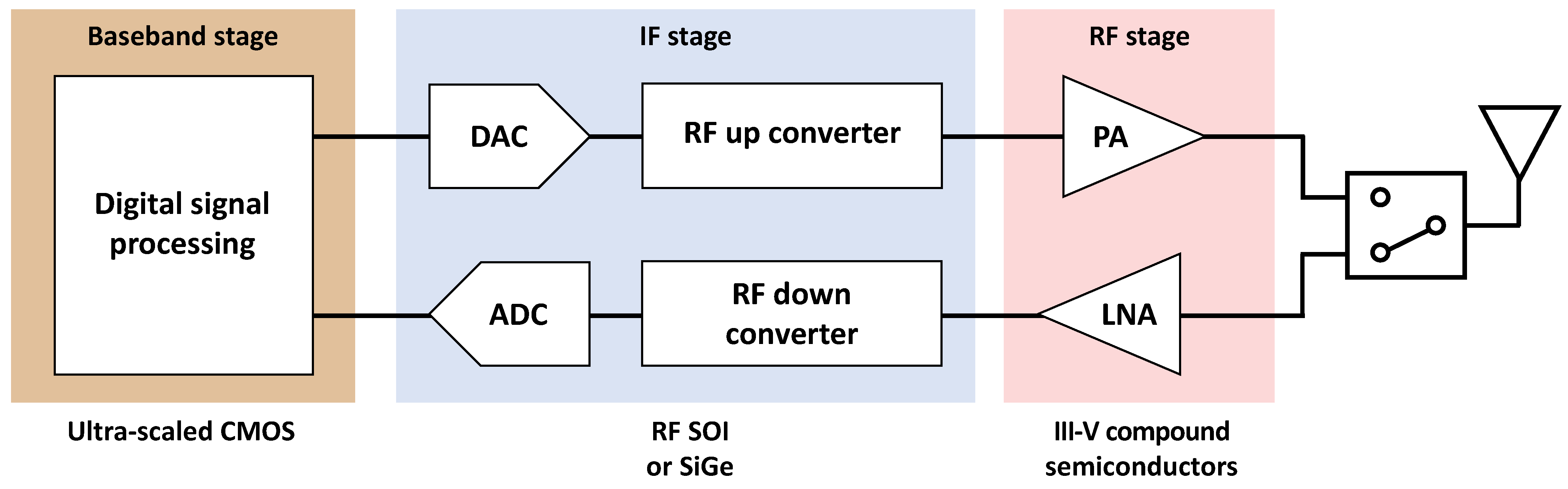
Therefore, to overcome the limitation of Si CMOS in high frequency and take advantage of highly advanced Si CMOS technology in digital, the heterogeneous integration of III-V and Si is required, as shown in Figure 3. In conventional heterogeneous integration, the III-V technology-based analog/RF circuits and Si CMOS technology-based digital circuits are fabricated respectively and integrated through packaging. However, the packaging technology has disadvantages, such as a long connection distance, high loss, high power consumption, and a large form factor. Furthermore, considering the development direction of the current wireless communication technology, massive multiple-input multiple-output (MIMO) and dense device integration are very important features one must take into account for hardware development [32,33]. For the application of Massive MIMO using a small antenna array, the requirement for the fine pitch size is increasing, and it is urgent to develop a technology that can achieve the micrometer level or less pitch size of I/O pins required for communication between the modules. According to the above trend, the packaging-based integration would be facing this technical difficulty, whereas the monolithic 3D integration process would be applicable for the finer pitch size as the integration density has been proven in other various applications (ex. Logic). Therefore, heterogeneous and monolithic 3D integration is essential for future wireless communication.
2.2. Heterogenous and Monolithic 3D Integration of III-V-Based RF Devices on Si CMOS
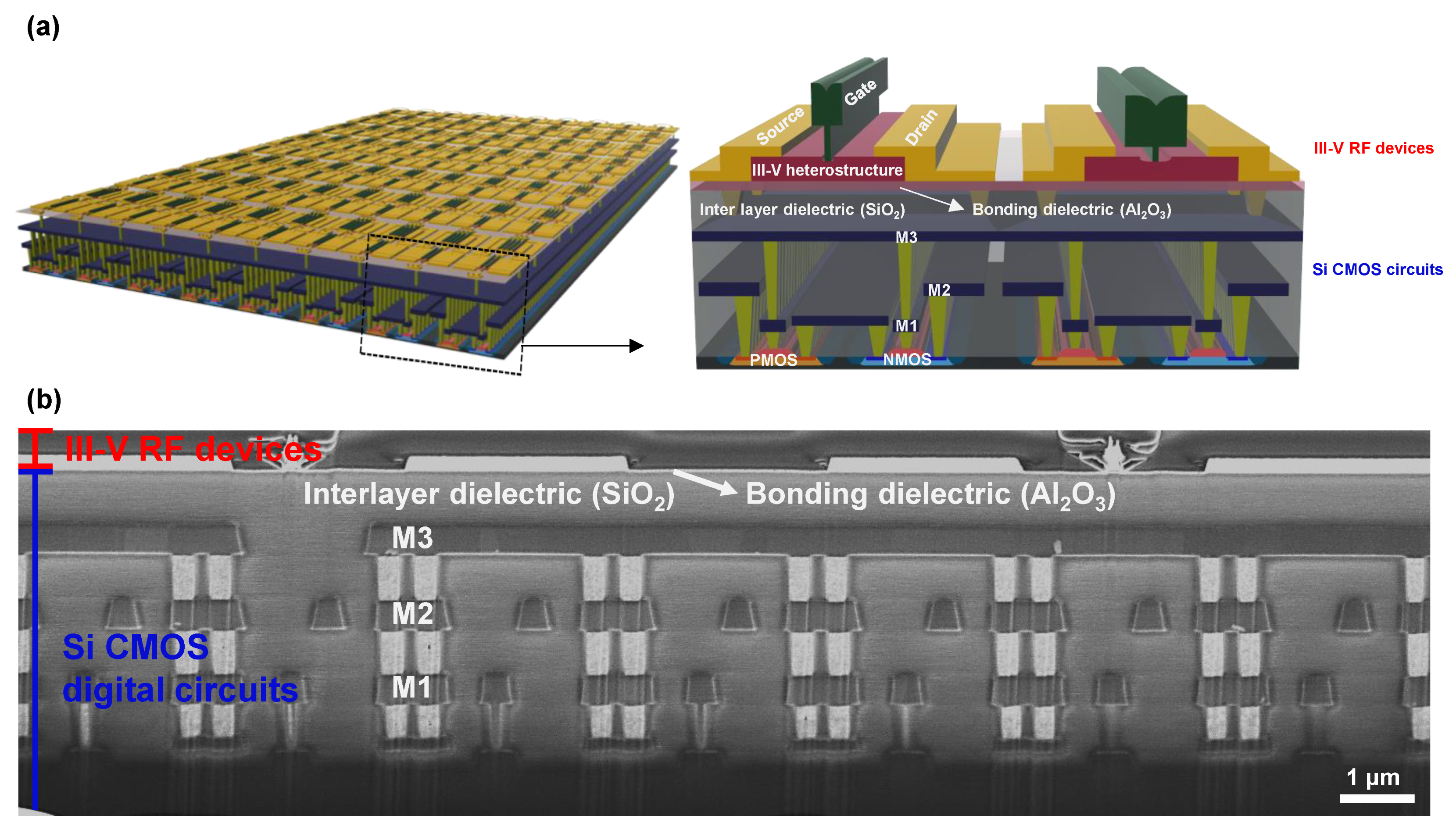
For future next-generation wireless communication, the co-integration of III-V-based RF devices and Si CMOS digital circuits is positively necessary, as shown in Figure 4a. We have successfully implemented the heterogeneous and monolithic 3D integration of III-V-based RF devices on Si CMOS by direct wafer bonding [10]. The cross-sectional SEM image is shown in Figure 4b. The III-V layers were uniformly bonded on Si CMOS. The top RF devices are based on InGaAs HEMT, and the bottom Si CMOS is a standard MOSFET structure with SiO2 gate dielectric and poly-Si gate. The heterogeneous and monolithic 3D integration process flow consists of (1) bottom Si CMOS fabrication with 180 nm standard CMOS technology, (2) back end of line (BEOL) process, (3) III-V heterostructure transfer by wafer bonding, (4) top device fabrication, (5) interconnect between top and bottom. Such monolithic 3D integration by direct wafer bonding enables tight integration of different technologies. The process temperature after the front end of the line (FEOL) of Si CMOS is very low at 300 °C or less [10,34]. Figure 5 shows the impact of monolithic 3D integration on the performance of bottom Si CMOS. The transistor characteristics, such as subthreshold swing, on current, off current, and threshold voltage, did not change after monolithic 3D integration, as shown in Figure 5a. Not only the characteristics of the individual transistor but also the function composed of several transistors showed almost no change in characteristics, as shown in Figure 5b. The thermal budget of 3D integration and top device fabrication is 300 °C, which is suitable for monolithic 3D integration.
We showed the basic concept of heterogeneous and monolithic 3D integrated III-V-based RF devices on Si CMOS circuits, as shown in Figure 6a. The top III-V-based RF devices consist of fT-oriented InGaAs HEMTs, which are designed to optimize the fT characteristic and fMAX-oriented InGaAs HEMTs, which are engineered to maximize the fMAX characteristic and bottom Si CMOS circuits are composed of the analog-to-digital converters (ADCs) and digital-to-analog converters (DACs). The fT-oriented InGaAs HEMT has a narrow head, and short gate stem, and the fMAX-oriented InGaAs HEMT features a wide head and short gate stem. The top RF device can amplify the high-frequency signals of hundreds of GHz because the III-V-based RF devices exhibit outstanding fT and fMAX, as shown in Figure 6b. At the same time, the bottom Si CMOS circuits of ADC and DAC can convert analog and digital signals to digital and analog signals, as shown in Figure 6c–h. A key feature of our heterogeneous and monolithic 3D integrated III-V-based RF devices on Si CMOS circuits is the ability to process analog/RF signals and digital signals with excellent performance at the same chip, utilizing different technologies (III-V and Si CMOS technology).
2.3. Issues on Monolithic 3D Integrated Analog/RF-Digital Mixed-Signal IC
2.3.1. Substrate Digital Interference
One of the critical issues in analog/RF-digital mixed-signal integrated circuits is electromagnetic coupling [35,36]. The monolithic integration of analog/RF circuits and digital circuits in the same chip induces the crosstalk between them. Therefore, the appropriate shielding technology is essential. Representatively, there is substrate digital interference in mixed-signal IC. The substrate digital interference, which is caused by switching any digital circuits, can be spread across the shared substrate and degrade the performance of analog/RF circuits when the digital circuits and analog/RF circuits are integrated on the same substrate. Therefore, in the traditional Si-based analog/RF-digital mixed-signal circuits, shielding technology, such as guard ring, deep N-well, deep trench isolation, and through silicon via (TSV), has been necessarily used [37,38]. However, these approaches require many additional process steps and occupy an additional area, imposing critical costs and area penalties. On the other hand, in the case of monolithic 3D integrated analog/RF-digital mixed-signal IC, the digital circuits and analog/RF circuits do not share the same substrate. These two different types of circuits are separated by an interlayer dielectric due to the inherent nature of the floating thin body structure of top devices. Therefore, it is expected that the digital interference from bottom digital circuits can be shielded and has no effect on top analog/RF circuits when an appropriate thickness of interlayer dielectric and BEOL lines are introduced.
To investigate the effect of substrate coupled digital interference in both conventional and monolithic 3D mixed-signal IC, we used a 31-stage ring oscillator in digital circuits as a signal source and a single transistor to sense the substrate digital interference in analog/RF circuits, as shown in Figure 7a. The schematics of the conventional and monolithic 3D mixed-signal systems are shown in Figure 7b,c. The top RF devices and bottom Si CMOS BEOL are separated with a 600-nm-thick interlayer dielectric. The results of substrate digital inference analysis are shown in Figure 7d,e. In the case of M3D mixed-signal IC, the bottom digital interference cannot propagate to the top circuits through the substrate because the digital and analog/RF circuits do not share the same substrate, whereas conventional 2D integrated transistors with the digital circuits strongly feel the digital interference when the digital circuits operate as in Figure 7d. This is another strong advantage of the M3D integration in mixed-signal IC.
2.3.2. Self-Heating
Another critical issue in monolithic 3D systems is the self-heating of top devices, which can affect the device’s performance. As reported by many research groups, the top devices are thermally isolated by an interlayer dielectric which has a low thermal conductivity, thereby, the performance and reliability can be degraded [39,40]. In the monolithic 3D system, the self-heating of the top device is one of the limiting factors in high performance, hence, many groups have reported on the self-heating effect in the M3D systems [39,40]. We presented one of the possible solutions to relaxing self-heating by introducing the metal plate, which has a high thermal conductivity at the backside of the top RF devices, as shown in Figure 8a [41,42]. The embedded metal can act as an additional heat dissipation path because the metal has high thermal conductivity. We used high-resolution thermoreflectance microscopy (TRM) to investigate the self-heating during the transistor operation [41,43]. Since variation in relative reflectivity (∆R/R) has a linear relationship with variation in surface temperature (∆T), the temperature of the device can be determined by detecting the change in reflectivity(R). The real-time thermal distribution of 3D integrated InGaAs-based RF transistors with different structures is shown in Figure 8b–e.
The 3D integrated InGaAs HEMTs with back metal show reduced self-heating characteristics compared to the 3D integrated InGaAs HEMTs without back metal because the back metal with high thermal conductivity offers an additional heat dissipation path, resulting in low static device temperature. The self-heating relaxing effect of the top devices increased as the size of the back metal increased, and the distance from the top device to the back metal decreased. However, the additional back parasitic capacitance is caused by the back metal. Moreover, when the metal is introduced near the top devices to relax the self-heating, the effect of back capacitance becomes more important, requiring careful device design to mitigate this trade-off relationship. The influence of the back metal on the RF performance of top devices was investigated [41]. However, a more systematic investigation of the influence of the back metal on the top RF devices in the M3D platform will be needed for successful heterogeneous and monolithic 3D integrated RF SoC.
2.4. Benchmarking of the Monolithic 3D Integrated RF Transistors
Many research groups have developed monolithic 3D integrated RF transistors. Figure 9 and Table 1 show the RF performance and information of the process to compare the state-of-the-art 3D integrated RF transistors [10,12,13,14,44,45,46,47,48]. The most important metric is cutoff frequency because it determines the maximum frequency at which the device can be used. As shown in Figure 9 the III-V-based RF devices, especially InGaAs-based RF transistors, obviously outperform Si transistors. This would motivate the heterogeneous and monolithic 3D integration in future wireless communication. Furthermore, the RF performance versus power consumption of the monolithic 3D integrated InGaAs on Si and monolithic 3D integrated Si on Si are shown in Figure 9. The monolithic 3D integrated InGaAs-based RF transistors on Si show higher RF performance at the same power consumption or less power consumption at the same RF performance than monolithic 3D integrated Si-based RF transistors on Si. This characteristic is also very important to be used for cryogenic LNA toward scalable quantum computing [49]. One drawback would be the fact that InGaAs-based devices are still difficult to be grown on large substrates, such as 200 or 300 mm sizes, resulting in a size mismatch to Si CMOS technology. The GaN-based devices overcome this problem by growing the GaN on Si wafers, but their RF performances fall short of InGaAs-based devices. Even in the case of InGaAs, it is thought that this problem can also be solved by introducing the growth of III-V on Si substrate or die to wafer bonding [50,51,52].
3. M3D Integration for High-Resolution III-V Image Sensors
Other than RF-SoCs, image sensors are one of the important applications for obtaining visual information in an autonomous car, time-of-flight sensors, and industrial surveillance systems [53,54,55]. Recently, 3-dimensional packaging using through-Si vias (TSVs) technology has been used to develop high-speed and high-resolution image sensors based on visible light absorption [56]. It is because there are several advantages, such as small chip size, high fill factor, and high bandwidth, whereas the conventional planar integration method, which places pixel region and pixel transistors and circuit section on the same plane, reduces the pixel area and an increases chip size, as shown in Figure 10 [5,57].
Although packaging technology has greatly accelerated the performance of image sensors, there is still room for improvement by full 3D integration with pixel transistors, etc. Therefore, ultimately, M3D integration can be a viable approach for future image sensors requiring much more functionalities. Beyond the visible light, detection of the short-wavelength infrared (SWIR) light has become increasingly important, which is mostly accomplished with the III-V material-based photodetectors (PDs) [55,56]. The packaging-based hybrid integration method currently used in III-V device integration with Si ICs has obvious limitations in terms of the resolution of several μm [56]. Thus, the benefits of M3D integration can be maximized in fabricating III-V image sensors because III-V materials can be processed at low temperatures, even a room temperature, and can be separated from donor substrates, making them very suitable for sequential fabrication [58,59]. Moreover, III-V thin film-based pixels can provide broadband detection capabilities with simple structure design, such as TMD/III-V heterojunction, Metal/III-V Schottky junction, III-V with optical mode resonance structure, etc. [60,61,62].
Here, we demonstrated the M3D integration of III-V-based PDs on SOI pixel transistors using CMOS-compatible fabrication processes, such as wafer-bonding and low-temperature sequential fabrication processes.
3.1. InGaAs Photodetectors on SOI-MOSFETs by Using Monolithic Integration and Sequential Fabrication Process
Figure 11 depicts the entire fabrication process flow for M3D InGaAs PDs on SOI-MOSFETs. SOI-MOSFETs have 50-nm Si channel thickness, 365-nm-thick BOX, and TiN/HfAlOx gate stack with a conventional InGaAs PD structure. Additionally, a chemical-mechanical polishing (CMP) process was used to obtain a flat surface for wafer bonding by depositing RF-sputtered SiO2 inter-layer dielectric (ILD) on SOI-MOSFET. The InGaAs PD structure was then bonded to SOI-MOSFETs by utilizing an intermediate layer of 40-nm-thick Al2O3 layer with oxygen plasma treatment. Then, the sequential fabrication process of InGaAs PD on SOI-MOSFET with various mesa dimensions was performed, indicating pixel pitch scalability of InGaAs PDs. We used the room-temperature process for M3D integration here, even without the contact annealing process of PDs. Finally, as shown in Figure 11h, the interconnection between InGaAs PD cathode and the source region of SOI-MOSFET was performed for 1 pixel/1-pixel transistor operation.
Figure 12a shows a low-magnification transmission electron microscopy (TEM) image of the M3D-integrated InGaAs PD on the SOI-MOSFET structure. Bottom SOI-MOSFET and top InGaAs PD layers were clearly seen to be free of voids and dislocations, indicating integration stability with only a low process temperature. Furthermore, the inset photograph of Figure 12a exhibits the actual fabrication of InGaAs PD on the 2 cm × 2 cm SOI-MOSFET chip with various dimensions of PD devices. These devices were formed by using a sequential fabrication process on the SOI-MOSFETs, implying that pixel pitch scaling could be facilitated by a lithographic alignment due to the elimination of a mechanical alignment used in TSVs and hybrid integration methods. In addition, energy dispersive X-ray (EDX) spectroscopy analysis was performed along with the red arrow, as shown in Figure 12a, to evaluate the bonding interface. The resulting EDX line profile was shown in Figure 12b for various atoms. We observed the formation of abrupt interfaces between different materials of InGaAs/Al2O3 and Al2O3/SiO2, suggesting our fabrication steps did not induce any interdiffusion of elements due to the low-temperature process.
Then, we performed the electrical and optical characterization of each device, as shown in Figure 12c,d, to confirm device performances of InGaAs PDs and SOI-MOSFETs before and after the M3D integration process. Figure 12c illustrates the transfer curves of the 9-μm gate length SOI-MOSFET with and without the M3D integration process. This evaluation is highly significant because the fabrication process of top layer devices can affect the bottom devices during the thermal processes and plasma process, etc. In our devices, there is a negligible difference in the subthreshold swing (S.S), on/off ratio, and saturation current of SOI-MOSFETs before and after M3D integration. It was confirmed that the top InGaAs devices process and integration process do not degrade the performance of the bottom devices. Moreover, the integrated InGaAs PD device has a good current ratio at ±1.5 V, corresponding to approximately 104 under dark conditions. Figure 12d shows a clear photoresponse with 0.7 A/W of responsivity without anti-reflection coating (ARC) obtained with 1550-nm laser illumination at the surface. From these results, top and bottom device qualities would be well preserved during the thin-film transfer process, and the device fabrication process that indicated the proposed M3D integration could be used to fabricate an actual M3D image sensor with a high resolution and a small chip size.
3.2. Evaluation of Fabricated InGaAs Photodetectors on SOI-MOSFETs for Mimicking IC Operation
Finally, we investigated the readout function for mimicking the actual ROIC operation using M3D integrated InGaAs PDs on SOI-MOSFETs. In actual ROIC operation, Figure 13a illustrates the fundamental building block of typical circuit configurations, such as direct injection and source-follower per detector [63]. Although IC operation mechanisms vary in many configurations, the basic element close to PDs is a simple combination of 1 PD and 1 Tr. Thus, we evaluated the fundamental function of IC operation in M3D integrated InGaAs PDs on SOI-MOSFETs (1PD and 1Tr structure). The readout voltage (Vout) measurement was performed for the top InGaAs PD layer under the illumination condition of a 1550 nm laser. Figure 13b shows the resulting Vout as a function of the light intensity by varying the gate bias (VGS) from 0.425 V to 1 V, where 0.425 V of VGS is in the subthreshold regime. This is due to the SOI-MOSFETs’ ability to function as a charge transfer gate in direct injection mode, where photo-generated carriers are directly injected via the source on the output stage. Vout gradually increased as VGS increased from 0.4 V to 1 V, which could be attributed to the division of resistance between Tr and PD caused by the Tr resistance decrease. Furthermore, in fixed VGS, increasing light intensity from 0.1 to 10 μW resulted in the Vout decrease due to PD resistance decrease. These results suggested the successful mixed-signal operation of the direct injection mechanism of ROIC by using M3D integrated PD and Tr structure. Recently, we demonstrated an M3D integrated MicroLED display on CMOS driver IC with a low-temperature process [17]. This integration process could be directly applied to integrated PD on ROIC in the future.
4. Conclusions
We presented the M3D integration-based InGaAs HEMTs and InGaAs PDs on Si-based bottom devices/ICs for next-generation RF and image sensor applications. For the RF applications, we demonstrated the heterogenous and monolithic 3D integration of III-V RF devices on Si CMOS circuits, which enable performance optimization in both RF and digital integrated circuits. Furthermore, we discussed the issues and solutions of substrate digital interference and self-heating in terms of the M3D integrated RF platform. For the image sensor applications, to overcome the inherent limitation of hybrid integration technology for fabricating high-resolution SWIR image sensors, the integrated 1 PD and 1 Tr devices successfully exhibited good PD performances after the layer transfer and fabrication process without bottom Si device degradations. Photolithographic alignment allowed dimension scaling, which can scale the pixel pitch to high-resolution (<1 μm). Furthermore, the basic IC operation changing from light signals to electrical signals was achieved. These results strongly suggested that the heterogeneous and monolithic 3D integration will provide high performance and multi-functionality in various applications, such as RF and image sensors.
Author Contributions
Conceptualization, methodology, analysis, J.J. and D.-M.G.; writing—original draft preparation; S.K. supervision of this paper. All authors have read and agreed to the published version of the manuscript.
Funding
This research was funded by the System Semiconductor Development Program funded by Gyeonggi-do, NRF of Korea (2022M3F3A2A01065057, 2022M3I8A107725711, 2020M3F3A2A02082450, 2020M3F3A2A01082329), NNFC OI LAB Project, and BrainKorea 21 (BK21) FOUR.
Conflicts of Interest
The authors declare no conflict of interest.
References
- Mallik, A.; Vandooren, A.; Witters, L.; Walke, A.; Franco, J.; Sherazi, Y.; Weckx, P.; Yakimets, D.; Bardon, M.; Parvais, B.; et al. The Impact of Sequential-3D Integration on Semiconductor Scaling Roadmap. In Proceedings of the 2018 IEEE International Electron Devices Meeting (IEDM), San Francisco, CA, USA, 1–5 December 2018. [Google Scholar] [CrossRef]
- Batude, P.; Brunet, L.; Fenouillet-Beranger, C.; Andrieu, F.; Colinge, J.P.; Lattard, D.; Vianello, E.; Thuries, S.; Billoint, O.; Vivet, P.; et al. 3D Sequential Integration: Application-Driven Technological Achievements and Guidelines. In Proceedings of the 2018 IEEE International Electron Devices Meeting (IEDM), San Francisco, CA, USA, 1–5 December 2018. [Google Scholar] [CrossRef]
- Shulaker, M.M.; Hills, G.; Park, R.S.; Howe, R.T.; Saraswat, K.; Wong, H.S.P.; Mitra, S. Three-Dimensional Integration of Nanotechnologies for Computing and Data Storage on a Single Chip. Nature 2017, 547, 74–78. [Google Scholar] [CrossRef] [PubMed]
- Motoyoshi, M. Through-Silicon Via (TSV). Proc. IEEE 2009, 97, 43–48. [Google Scholar] [CrossRef]
- Haruta, T.; Nakajima, T.; Hashizume, J.; Umebayashi, T.; Takahashi, H.; Taniguchi, K.; Kuroda, M.; Sumihiro, H.; Enoki, K.; Yamasaki, T.; et al. A 1/2.3inch 20Mpixel 3-Layer Stacked CMOS Image Sensor with DRAM. In Proceedings of the 2017 IEEE International Solid-State Circuits Conference (ISSCC), San Francisco, CA, USA, 5–9 February 2017. [Google Scholar] [CrossRef]
- Estrada, J.A.; Lasser, G.; Pinto, M.; Herrault, F.; Popovic, Z. Metal-Embedded Chip Assembly Processing for Enhanced RF Circuit Performance. IEEE Trans. Microw. Theory Tech. 2019, 67, 3537–3546. [Google Scholar] [CrossRef]
- Herrault, F.; Wong, J.; Ramos, I.; Tai, H.; King, M. Chiplets in Wafers (CiW) Process Design Kit and Demonstration of High-Frequency Circuits with GaN Chiplets in Silicon Interposers. In Proceedings of the 2021 IEEE 71st Electronic Components and Technology Conference (ECTC), San Diego, CA, USA, 1–4 June 2021. [Google Scholar] [CrossRef]
- Weimann, N.; Hossain, M.; Krozer, V.; Heinrich, W.; Lisker, M.; Mai, A. Tight Focous Toward the Future: Tight Material Combination for Millimeter-Wave RF Power Applications: InP HBT SiGe BiCMOS Heterogeneous Wafer-Level Integration. IEEE Microw. Mag. 2017, 18, 74–82. [Google Scholar] [CrossRef]
- Urteaga, M.; Carter, A.; Griffith, Z.; Pierson, R.; Bergman, J.; Arias, A.; Rowell, P.; Hacker, J.; Brar, B.; Rodwell, M.J.W. THz Bandwidth InP HBT Technologies and Heterogeneous Integration with Si CMOS. In Proceedings of the 2016 IEEE Bipolar/BiCMOS Circuits and Technology Meeting (BCTM), New Brunswick, NJ, USA, 25–27 September 2016. [Google Scholar] [CrossRef]
- Jeong, J.; Kim, S.K.; Kim, J.; Geum, D.M.; Kim, D.; Jo, E.; Jeong, H.; Park, J.; Jang, J.H.; Choi, S.; et al. Heterogeneous and Monolithic 3D Integration of III-V-Based Radio Frequency Devices on Si CMOS Circuits. ACS Nano 2022, 16, 9031–9040. [Google Scholar] [CrossRef] [PubMed]
- Jeong, J.; Kim, S.K.; Kim, J.; Geum, D.; Park, J.; Jang, J.; Kim, S. High-Performance InGaAs-On-Insulator HEMTs on Si CMOS for Substrate Coupling Noise-Free Monolithic 3D Mixed-Signal IC. In Proceedings of the 2021 IEEE Symposium on VLSI Technology, Kyoto, Japan, 13–19 June 2021. [Google Scholar]
- Caimi, D.; Tiwari, P.; Sousa, M.; Moselund, K.E.; Zota, C.B. Heterogeneous Integration of III-V Materials by Direct Wafer Bonding for High-Performance Electronics and Optoelectronics. IEEE Trans. Electron Devices 2021, 68, 3149–3156. [Google Scholar] [CrossRef]
- Frutuoso, T.M.; Sideris, P.; Lugo-Alvarez, J.; Garros, X.; Brunet, L.; Fenouille-Beranger, C.; Batude, P.; Theodorou, C.; Ferrari, P.; Gaillard, F. RF Performance of Devices Processed in Low-Temperature Sequential Integration. IEEE Trans. Electron Devices 2021, 68, 3157–3162. [Google Scholar] [CrossRef]
- Vandooren, A.; Franco, J.; Parvais, B.; Wu, Z.; Witters, L.; Walke, A.; Li, W.; Peng, L.; Desphande, V.; Bufler, F.M.; et al. 3D Sequential Stacked Planar Devices on 300 Mm Wafers Featuring Replacement Metal Gate Junction-Less Top Devices Processed at 525 °C with Improved Reliability. In Proceedings of the 2018 IEEE Symposium on VLSI Technology, Honolulu, HI, USA, 18–22 June 2018. [Google Scholar] [CrossRef]
- Geum, D.M.; Kim, S.K.; Lee, S.; Lim, D.; Kim, H.J.; Choi, C.H.; Kim, S.H. Monolithic 3D Integration of InGaAs Photodetectors on Si MOSFETs Using Sequential Fabrication Process. IEEE Electron Device Lett. 2020, 41, 433–436. [Google Scholar] [CrossRef]
- Kim, S.K.; Geum, D.M.; Lim, H.R.; Han, J.; Kim, H.; Jeong, Y.; Kim, S.H. Photo-Responsible Synapse Using Ge Synaptic Transistors and GaAs Photodetectors. IEEE Electron Device Lett. 2020, 41, 605–608. [Google Scholar] [CrossRef]
- Park, J.; Geum, D.M.; Baek, W.; Shieh, J.; Kim, S. Monolithic 3D sequential integration realizing 1600-PPI red micro-LED display on Si CMOS driver IC. In Proceedings of the 2022 IEEE Symposium on VLSI Technology and Circuits (VLSI Technology and Circuits), Honolulu, HI, USA, 12–17 June 2022. [Google Scholar] [CrossRef]
- Kim, S.K.; Jeong, Y.; Bidenko, P.; Lim, H.R.; Jeon, Y.R.; Kim, H.; Lee, Y.J.; Geum, D.M.; Han, J.; Choi, C.; et al. 3D Stackable Synaptic Transistor for 3D Integrated Artificial Neural Networks. ACS Appl. Mater. Interfaces 2020, 12, 7372–7380. [Google Scholar] [CrossRef]
- Han, J.K.; Sim, J.; Geum, D.M.; Kim, S.K.; Yu, J.M.; Kim, J.; Kim, S.; Choi, Y.K. 3D Stackable Broadband Photoresponsive InGaAs Biristor Neuron for a Neuromorphic Visual System with Near 1 v Operation. In Proceedings of the 2021 IEEE International Electron Devices Meeting (IEDM), San Francisco, CA, USA, 11–16 December 2021. [Google Scholar] [CrossRef]
- Lee, H.J.; Rami, S.; Ravikumar, S.; Neeli, V.; Phoa, K.; Sell, B.; Zhang, Y. Intel 22nm FinFET (22FFL) Process Technology for RF and Mm Wave Applications and Circuit Design Optimization for FinFET Technology. In Proceedings of the 2018 IEEE International Electron Devices Meeting (IEDM), San Francisco, CA, USA, 1–5 December 2018. [Google Scholar] [CrossRef]
- Kane, O.M.; Lucci, L.; Scheiblin, P.; Lepilliet, S.; Danneville, F. 22nm Ultra-Thin Body and Buried Oxide FDSOI RF Noise Performance. In Proceedings of the 2019 IEEE Radio Frequency Integrated Circuits Symposium (RFIC), Boston, MA, USA, 2–4 June 2019. [Google Scholar] [CrossRef]
- Van Der Voorn, P.; Agostinelli, M.; Choi, S.J.; Curello, G.; Deshpande, H.; El-Tanani, M.A.; Hafez, W.; Jalan, U.; Janbay, L.; Kang, M.; et al. A 32nm Low Power RF CMOS SOC Technology Featuring High-k/Metal Gate. In Proceedings of the 2010 Symposium on VLSI Technology, Honolulu, HI, USA, 15–17 June 2010. [Google Scholar] [CrossRef]
- Vandooren, A.; Parvais, B.; Witters, L.; Walke, A.; Vais, A.; Merckling, C.; Lin, D.; Waldron, N.; Wambacq, P.; Mocuta, D.; et al. 3D Technologies for Analog/RF Applications. In Proceedings of the IEEE SOI-3D-Subthreshold Microelectronics Technology Unified Conference (S3S), Burlingame, CA, USA, 16–19 October 2017. [Google Scholar] [CrossRef]
- Collaert, N.; Alian, A.; Banerjee, A.; Chauhan, V.; Elkashlan, R.Y.; Hsu, B.; Ingels, M.; Khaled, A.; Kodandarama, K.V.; Kunert, B.; et al. From 5G to 6G: Will Compound Semiconductors Make the Difference? In Proceedings of the 2020 IEEE 15th International Conference Solid-State Integration Circuit Technol. ICSICT, Kunning, China, 3–6 November 2020. [Google Scholar] [CrossRef]
- Parvais, B.; Vais, A.; Yadav, S.; Mols, Y.; Vermeersch, B.; Kodanarama, K.V.; Boccardi, G.; Kunert, B.; Collaert, N. III-V on a Si Platform for the next Generations of Communication Systems. In Proceedings of the 2022 6th IEEE Electron Devices Technology and Manufacturing Conference (EDTM), Oita, Japan, 6–9 March 2022. [Google Scholar] [CrossRef]
- Green, D.S.; Dohrman, C.L.; Demmin, J.; Chang, T.H. Path to 3D Heterogeneous Integration. In Proceedings of the 2015 International 3D Systems Integration Conference, Sendai, Japan, 31 August–2 September 2015. [Google Scholar] [CrossRef]
- Heinemann, B.; Rucker, H.; Barth, R.; Barwolf, F.; Drews, J.; Fischer, G.G.; Fox, A.; Fursenko, O.; Grabolla, T.; Herzel, F.; et al. SiGe HBT with Fx/Fmax of 505 GHz/720 GHz. In Proceedings of the 2016 IEEE International Electron Devices Meeting (IEDM), San Francisco, CA, USA, 3–7 December 2016. [Google Scholar] [CrossRef]
- Lai, R.; Mei, X.B.; Deal, W.R.; Yoshida, W.; Kim, Y.M.; Liu, P.H.; Lee, J.; Uyeda, J.; Radisic, V.; Lange, M.; et al. Sub 50 nm InP HEMT Device with Fmax Greater than 1 THz. In Proceedings of the 2007 IEEE International Electron Devices Meeting, Washington, DC, USA, 10–12 December 2007. [Google Scholar] [CrossRef]
- Mei, X.; Yoshida, W.; Lange, M.; Lee, J.; Zhou, J.; Liu, P.H.; Leong, K.; Zamora, A.; Padilla, J.; Sarkozy, S.; et al. First Demonstration of Amplification at 1 THz Using 25-nm InP High Electron Mobility Transistor Process. IEEE Electron Device Lett. 2015, 36, 327–329. [Google Scholar] [CrossRef]
- Jo, H.B.; Yun, S.W.; Kim, J.G.; Baek, J.M.; Lee, I.G.; Kim, D.H.; Kim, T.W.; Kim, S.K.; Yun, J.; Kim, T.; et al. Sub-30-nm In0.8Ga0.2As Composite-Channel High-Electron-Mobility Transistors with Record High-Frequency Characteristics. IEEE Trans. Electron Devices 2021, 68, 2010–2016. [Google Scholar] [CrossRef]
- Thome, F.; Heinz, F.; Leuther, A. InGaAs MOSHEMT W-Band LNAs on Silicon and Gallium Arsenide Substrates. IEEE Microw. Wirel. Compon. Lett. 2020, 30, 1089–1092. [Google Scholar] [CrossRef]
- Larsson, E.G.; Edfors, O.; Tufvesson, F.; Marzetta, T.L. Massive MIMO for next Generation Wireless Systems. IEEE Commun. Mag. 2014, 52, 186–195. [Google Scholar] [CrossRef]
- Lu, L.; Li, G.Y.; Swindlehurst, A.L.; Ashikhmin, A.; Zhang, R. An Overview of Massive MIMO: Benefits and Challenges. IEEE J. Sel. Top. Signal Process. 2014, 8, 742–758. [Google Scholar] [CrossRef]
- Jeong, J.; Kim, S.K.; Kim, J.; Geum, D.M.; Park, J.; Jang, J.H.; Kim, S. Stackable InGaAs-on-Insulator HEMTs for Monolithic 3-D Integration. IEEE Trans. Electron Devices 2021, 68, 2205–2211. [Google Scholar] [CrossRef]
- Su, D.K.; Loinaz, M.J.; Masui, S.; Wooley, B.A. Experimental Results and Modeling Techniques for Substrate Noise in Mixed-Signal Integrated Circuits. IEEE J. Solid-State Circuits 1993, 28, 420–429. [Google Scholar] [CrossRef]
- Xu, M.; Su, D.K.; Shaeffer, D.K.; Lee, T.H.; Wooley, B.A. Measuring and Modeling the Effects of Substrate Noise on the LNA for a CMOS GPS Receiver. IEEE J. Solid-State Circuits 2001, 36, 473–485. [Google Scholar] [CrossRef]
- Kosaka, D.; Nagata, M.; Hiraoka, Y.; Imanoshi, I.; Maeda, M.; Murasaka, Y.; Iwata, A. Isolation Strategy Against Substrate Coupling in CMOS Mixed-Signal/RF Circuits. In Proceedings of the 2005 Symposium on VLSI Circuits, Kyoto, Japan, 16–18 July 2005. [Google Scholar] [CrossRef]
- Uemura, S.; Hiraoka, Y.; Kai, T.; Dosho, S. Isolation Techniques Against Substrate Noise Coupling Utilizing Through Silicon Via (TSV) Process for RF/Mixed-Signal SoCs. IEEE J. Solid-State Circuits 2012, 47, 810–816. [Google Scholar] [CrossRef]
- Shin, S.H.; Kim, S.H.; Kim, S.; Wu, H.; Ye, P.D.; Alam, M.A. Substrate and Layout Engineering to Suppress Self-Heating in Floating Body Transistors. In Proceedings of the 2016 IEEE International Electron Devices Meeting (IEDM), San Francisco, CA, USA, 3–7 December 2016. [Google Scholar] [CrossRef]
- Triantopoulos, K.; Casse, M.; Brunet, L.; Batude, P.; Fenouillet-Beranger, C.; Mathieu, B.; Vinet, M.; Ghibaudo, G.; Reimbold, G. Thermal effects in 3D sequential technology. In Proceedings of the 2017 IEEE International Electron Devices Meeting (IEDM), San Francisco, CA, USA, 2–6 December 2017. [Google Scholar] [CrossRef]
- Jeong, J.; Kim, S.K.; Kim, J.; Geum, D.M.; Kim, S. Monolithic 3D Integrated InGaAs HEMTs on Si for Next-Generation Communication: Record {MAX} and Relaxed Self-Heating of Top Devices by a Novel M3D Structure. In Proceedings of the 2021 IEEE International Electron Devices Meeting (IEDM), San Francisco, CA, USA, 11–16 December 2021. [Google Scholar] [CrossRef]
- Jeong, J.; Kim, S.K.; Kim, J.; Geum, D.-M.; Kim, S. Heat Management in Monolithic 3D RF Platform. In Proceedings of the 2022 6th IEEE Electron Devices Technology & Manufacturing Conference (EDTM), Oita, Japan, 6–9 March 2022. [Google Scholar] [CrossRef]
- Shim, J.; Lim, J.; Geum, D.M.; You, J.B.; Yoon, H.; Kim, J.P.; Baek, W.J.; Han, J.H.; Kim, S. TiOx/Ti/TiOx Tri-Layer Film-Based Waveguide Bolometric Detector for On-Chip Si Photonic Sensor. IEEE Trans. Electron Devices 2022, 69, 2151–2158. [Google Scholar] [CrossRef]
- Zota, C.B.; Convertino, C.; Baumgartner, Y.; Sousa, M.; Caimi, D.; Czornomaz, L. High Performance Quantum Well InGaAs-On-Si MOSFETs with Sub-20 nm Gate Length for RF Applications. In Proceedings of the 2018 IEEE International Electron Devices Meeting (IEDM), San Francisco, CA, USA, 1–5 December 2018. [Google Scholar] [CrossRef]
- Tessmann, A.; Leuther, A.; Heinz, F.; Bernhardt, F.; John, L.; Massler, H.; Czornomaz, L.; Merkle, T. 20-nm In0.8Ga0.2As MOSHEMT MMIC Technology on Silicon. IEEE J. Solid-State Circuits 2019, 54, 2411–2418. [Google Scholar] [CrossRef]
- Yadav, S.; Kumar, A.; Nguyen, X.S.; Lee, K.H.; Liu, Z.; Xing, W.; Masudy-Panah, S.; Lee, K.; Tan, C.S.; Fitzgerald, E.A.; et al. High Mobility In0.30Ga0.70As MOSHEMTs on Low Threading Dislocation Density 200 mm Si Substrates: A Technology Enabler Towards Heterogenous Integration of Low Noise and Medium Power Amplfiers with Si CMOS. In Proceedings of the 2017 IEEE International Electron Devices Meeting (IEDM), San Francisco, CA, USA, 2–6 December 2017. [Google Scholar] [CrossRef]
- Then, H.W.; Radosavljevic, M.; Koirala, P.; Thomas, N.; Nair, N.; Ban, I.; Talukdar, T.; Nordeen, P.; Ghosh, S.; Bader, S.; et al. Advanced Scaling of Enhancement Mode High-K Gallium Nitride-on-300mm-Si(111) Transistor and 3D Layer Transfer GaN-Silicon Finfet CMOS Integration. In Proceedings of the 2021 IEEE International Electron Devices Meeting (IEDM), San Francisco, CA, USA, 11–16 December 2021. [Google Scholar] [CrossRef]
- Parvais, B.; Alian, A.; Peralagu, U.; Rodriguez, R.; Yadav, S.; Khaled, A.; Elkashlan, R.Y.; Putcha, V.; Sibaja-Hernandez, A.; Zhao, M.; et al. GaN-on-Si Mm-Wave RF Devices Integrated in a 200mm CMOS Compatible 3-Level Cu BEOL. In Proceedings of the 2020 IEEE International Electron Devices Meeting (IEDM), San Francisco, CA, USA, 12–18 December 2020. [Google Scholar] [CrossRef]
- Jeong, J.; Kim, S.K.; Kim, J.; Geum, D.; Lee, J.; Park, S.; Kim, S. 3D Stackable Cryogenic InGaAs HEMTs for Heterogeneous and Monolithic 3D Integrated Highly Scalable Quantum Computing Systems. In Proceedings of the 2022 IEEE Symposium on VLSI Technology and Circuits (VLSI Technology and Circuits), Honolulu, HI, USA, 12–17 June 2022. [Google Scholar] [CrossRef]
- Kim, S.H.; Ikku, Y.; Yokoyama, M.; Nakane, R.; Li, J.; Kao, Y.C.; Takenaka, M.; Takagi, S. High Performance InGaAs-on-Insulator MOSFETs on Si by Novel Direct Wafer Bonding Technology Applicable to Large Wafer Size. In Proceedings of the 2014 Symposium on VLSI Technology (VLSI-Technology), Honolulu, HI, USA, 9–12 June 2014. [Google Scholar] [CrossRef]
- Uhrmann, T.; Burggraf, J.; Eibelhuber, M. Heterogeneous Integration by Collective Die-to-Wafer Bonding. In Proceedings of the 2018 International Wafer Level Packaging Conference (IWLPC), San Hose, CA, USA, 23–25 October 2018. [Google Scholar] [CrossRef]
- Lee, S.; Kim, S.K.; Han, J.H.; Song, J.D.; Jun, D.H.; Kim, S.H. Epitaxial Lift-Off Technology for Large Size III-V-on-Insulator Substrate. IEEE Electron Device Lett. 2019, 40, 1732–1735. [Google Scholar] [CrossRef]
- Choi, B.S.; Kim, S.H.; Lee, J.; Chang, S.; Park, J.; Lee, S.J.; Shin, J.K. CMOS Image Sensor Using Pixel Aperture Technique for Single-Chip 2D and 3D Imaging. In Proceedings of the 2017 IEEE SENSORS, Glasgow, UK, 29 October–1 November 2017. [Google Scholar] [CrossRef]
- Lange, R.; Seitz, P. Solid-State Time-of-Flight Range Camera. IEEE J. Quantum Electron. 2001, 37, 390–397. [Google Scholar] [CrossRef]
- Geum, D.M.; Kim, S.; Kim, S.K.; Kang, S.; Kyhm, J.; Song, J.; Choi, W.J.; Yoon, E. Monolithic Integration of Visible GaAs and Near-Infrared InGaAs for Multicolor Photodetectors by Using toward High-Resolution Imaging Systems. Sci. Rep. 2019, 9, 18661. [Google Scholar] [CrossRef] [PubMed]
- Manda, S.; Zaizen, Y.; Hirano, T.; Iwamoto, H.; Matsumoto, R.; Saito, S.; Maruyama, S.; Minari, H.; Hirano, T.; Takachi, T.; et al. High-Definition Visible-SWIR InGaAs Image Sensor Using Cu-Cu Bonding of III-V to Silicon Wafer. In Proceedings of the 2019 IEEE International Electron Devices Meeting (IEDM), San Francisco, CA, USA, 7–11 December 2019. [Google Scholar] [CrossRef]
- Xu, K. Integrated Silicon Directly Modulated Light Source Using P-Well in Standard CMOS Technology. IEEE Sens. J. 2016, 16, 6184–6191. [Google Scholar] [CrossRef]
- Kim, S.H.; Kim, S.K.; Shim, J.P.; Geum, D.M.; Ju, G.; Kim, H.S.; Lim, H.J.; Lim, H.R.; Han, J.H.; Lee, S.; et al. Heterogeneous Integration Toward a Monolithic 3-D Chip Enabled by III-V and Ge Materials. IEEE J. Electron Devices Soc. 2018, 6, 579–587. [Google Scholar] [CrossRef]
- Kim, S.K.; Shim, J.P.; Geum, D.M.; Kim, C.Z.; Kim, H.S.; Song, J.D.; Choi, S.J.; Kim, D.H.; Choi, W.J.; Kim, H.J.; et al. Fabrication of InGaAs-on-Insulator Substrates Using Direct Wafer-Bonding and Epitaxial Lift-Off Techniques. IEEE Trans. Electron Devices 2017, 64, 3601–3608. [Google Scholar] [CrossRef]
- Jang, J.H.; Geum, D.M.; Kim, S.H. Broadband Au/n-GaSb Schottky photodetector array with a spectral range from 300 nm to 1700 nm. Opt. Express 2021, 29, 38894–38903. [Google Scholar] [CrossRef]
- Geum, D.M.; Kim, S.; Khym, J.; Lim, J.; Kim, S.; Ahn, S.Y.; Kim, T.S.; Kang, K.; Kim, S.H. Arrayed MoS2–In0.53Ga0.47As van der Waals Heterostructure for High-Speed and Broadband Detection from Visible to Shortwave-Infrared Light. Small 2021, 17, 2007357. [Google Scholar] [CrossRef]
- Geum, D.M.; Lim, J.; Jang, J.; Ahn, S.Y.; Kim, S.K.; Shim, J.; Kim, B.H.; Park, J.H.; Baek, W.J.; Jeong, J.; et al. A sub-micron-thick InGaAs broadband (400-1700 nm) photodetectors with a high external quantum efficiency (>70%). In Proceedings of the 2022 IEEE Symposium on VLSI Technology and Circuits (VLSI Technology and Circuits), Honolulu, HI, USA, 12–17 June 2022. [Google Scholar] [CrossRef]
- Bielecki, Z. Readout electronics for optical detectors. OPTO-Electron. Rev. 2004, 12, 129–137. [Google Scholar]
Figure 1.
Conceptual illustration of heterogeneous and monolithic 3D integrated system including digital logic (blue layer, Si technology), analog/RF (red layer, III-V technology), and sensor (green layer, III-V technology).
Figure 1.
Conceptual illustration of heterogeneous and monolithic 3D integrated system including digital logic (blue layer, Si technology), analog/RF (red layer, III-V technology), and sensor (green layer, III-V technology).

Figure 2.
The (a) fT and (b) fMAX versus technology node of the state-of-the-art RF transistors.

Figure 3.
The strategy of heterogeneous integration in RF chips to optimize the performance in both digital and analog/RF circuits.
Figure 3.
The strategy of heterogeneous integration in RF chips to optimize the performance in both digital and analog/RF circuits.

Figure 4.
(a) Schematic of heterogeneous and monolithic 3D integrated III-V-based RF devices in Si CMOS. (b) Cross-sectional STEM image of top transistor based on InGaAs HEMT. Reprinted with permission from Ref. [10]. 2022, ACS Nano.
Figure 4.
(a) Schematic of heterogeneous and monolithic 3D integrated III-V-based RF devices in Si CMOS. (b) Cross-sectional STEM image of top transistor based on InGaAs HEMT. Reprinted with permission from Ref. [10]. 2022, ACS Nano.

Figure 5.
(a) Transfer characteristics of bottom single Si MOSFET before and after monolithic 3D integration. (b) Output waveform of VCO based on a ring oscillator composed of multiple Si MOSFETs.Reprinted with permission from Ref. [10]. 2022, ACS Nano.
Figure 5.
(a) Transfer characteristics of bottom single Si MOSFET before and after monolithic 3D integration. (b) Output waveform of VCO based on a ring oscillator composed of multiple Si MOSFETs.Reprinted with permission from Ref. [10]. 2022, ACS Nano.

Figure 6.
(a) Conceptual schematic of heterogeneous and monolithic 3D integrated III-V-based RF devices on Si CMOS. (b) Gain plot of fT and fMAX-oriented top InGaAs HEMTs. (c) The block diagram of ADC. (d) Time domain output voltage of ADC. (e) Digital output of ADC. (f) The block diagram of DAC. (g) Analog output of DAC. (h) Sinewave output of DAC. Reprinted with permission from Ref. [10]. 2022, ACS Nano.

Figure 7.
(a) Substrate digital interference measurement setup. The schematic of (b) conventional and (c) monolithic 3D integrated digital-analog/RF mixed-signal IC. The result of substrate digital interference analysis in (d) conventional and (e) monolithic 3D integrated digital-analog/RF mixed-signal IC. Reprinted with permission from Ref. [11]. 2021, JSAP.

Figure 8.
(a) Conceptual schematic of heterogeneous and monolithic 3D integrated III-V-based RF device on Si CMOS with back metal to relax the self-heating of top devices. The arrows represent the heat spread. The (b) schematics, (c) cross-sectional images, (d) CCD, and (e) thermal images of 3D integrated InGaAs HEMTs with different structures. Reprinted with permission from Ref. [41]. 2022, IEEE.

Figure 9.
(a) The important FOMs of fT and fMAX are shown with different types of state-of-the-art monolithic 3D RF transistors. The (b) fT and (c) fMAX versus power consumption of InGaAs on Si and Si on Si. The best performances of each technology were used for comparison.
Figure 9.
(a) The important FOMs of fT and fMAX are shown with different types of state-of-the-art monolithic 3D RF transistors. The (b) fT and (c) fMAX versus power consumption of InGaAs on Si and Si on Si. The best performances of each technology were used for comparison.

Figure 10.
The development trend for fabricating image sensors from conventional planar integration method to newly 3D vertical integration including pixel area, pixel transistors, and image signal processor (ISP).
Figure 10.
The development trend for fabricating image sensors from conventional planar integration method to newly 3D vertical integration including pixel area, pixel transistors, and image signal processor (ISP).

Figure 11.
The fabrication process of vertically integrated InGaAs PDs on SOI-MOSFETs. (a) SOI substrate preparation. (b) Fabrication of SOI MOSFETs with TiN gate and HfAlOx. (c) SiO2 deposition and CMP process for planarization. (d) Al2O3 deposition for MOSFETs and PDs for wafer bonding. (e) Wafer bonding with plasma treatment. (f) InP substrate removal by using HCl solution. (g) Se-quentially processed InGaAs PDs. (h) Interconnection from cathode of PDs to sources of MOSFETs by filling via holes. Reprinted with permission from Ref. [15]. 2020, IEEE.

Figure 12.
(a) Cross-sectional low-magnified TEM image of InGaAs PDs on SOI-MOSFETs with SiO2 ILD layer and inset photograph for an actual chip. The red arrow is the EDX scan line. (b) EDX line profile of various atoms of In, Ga, As, Si, O, and Al along to the red arrow in Figure 11a. (c) The transfer curves of SOI-MOSFET with 9-μm gate length before and after monolithic 3D integration. (d) Current-voltage characteristics of InGaAs PD with a 1550-nm laser under dark/light conditions. The current is increased after laser illumination. Reprinted with permission from Ref. [15]. 2022, IEEE.

Figure 13.
(a) The measured unit cell for readout operation for the fabricated InGaAs PD on SOI-MOSFET for mimicking the direct injection operation. (b) Electrical responses of the measured unit cell with various gate biases and light intensity on top InGaAs PDs. Reprinted with permission from Ref. [15]. 2022, IEEE.


Table 1.
Comparison of M3D RF transistors.
| RF Device | Tprocess of RF Device | LG | fT/fMAX | Integration with Si CMOS | ||
|---|---|---|---|---|---|---|
| KAIST [10] | InGaAs HEMT | ≤300 °C | 80 nm (fMAX oriented design) | 329/742 GHz | 494 GHz | Yes |
| 140 nm (fT oriented design) | 448/213 GHz | 309 GHz | ||||
| IBM [43] | InGaAs MOSFET | ≤500 °C | 20 nm | 380/310 GHz | 343 GHz | No |
| IBM [12] | InGaAs MOSFET | ≤500 °C | 25 nm | 210/200 GHz | 205 GHz | Yes |
| Fraunhofer IAF [44] | InGaAs MOSHEMT | ≤300 °C | 20 nm | 640/200 GHz | 358 GHz | No |
| NUS [45] | InGaAs MOSHEMT | ≤350 °C | 150 nm | 60/- GHz | - | Yes |
| Intel [46] | GaN MOSHEMT | - | 30 nm | 300/400 GHz | 346 GHz | Yes |
| IMEC [47] | GaN HEMT | - | 110 nm | 56/135 GHz | 87 GHz | No |
| IMEC [14] | Si MOSFET | ≤525 °C | 80 nm | 80/115 GHz | 96 GHz | No |
| LETI [13] | Si MOSFET | ≤500 °C | 45 nm | 105/175 GHz | 136 GHz | No |
Publisher’s Note: MDPI stays neutral with regard to jurisdictional claims in published maps and institutional affiliations. |
© 2022 by the authors. Licensee MDPI, Basel, Switzerland. This article is an open access article distributed under the terms and conditions of the Creative Commons Attribution (CC BY) license (https://creativecommons.org/licenses/by/4.0/).
Share and Cite
MDPI and ACS Style
Jeong, J.; Geum, D.-M.; Kim, S. Heterogeneous and Monolithic 3D Integration Technology for Mixed-Signal ICs. Electronics 2022, 11, 3013. https://doi.org/10.3390/electronics11193013
AMA Style
Jeong J, Geum D-M, Kim S. Heterogeneous and Monolithic 3D Integration Technology for Mixed-Signal ICs. Electronics. 2022; 11(19):3013. https://doi.org/10.3390/electronics11193013
Chicago/Turabian StyleJeong, Jaeyong, Dae-Myeong Geum, and SangHyeon Kim. 2022. "Heterogeneous and Monolithic 3D Integration Technology for Mixed-Signal ICs" Electronics 11, no. 19: 3013. https://doi.org/10.3390/electronics11193013
Note that from the first issue of 2016, this journal uses article numbers instead of page numbers. See further details here.